CY14V101PS
1-Mbit (128K × 8) Quad SPI nvSRAM with
Real Time Clock
Features
■
Temperature range
❐ Industrial: –40 °C to 85 °C
Packages
❐ 16-pin SOIC
■
Density
❐ 1 Mbit (128K × 8)
■
■
Bandwidth
❐ 108-MHz high-speed interface
❐ Read and write at 54 MBps
Functional Overview
■
Serial Peripheral Interface
❐ Clock polarity and phase modes 0 and 3
❐ Multi I/O option – Single SPI (SPI), Dual SPI (DPI), and Quad
SPI (QPI)
■
High reliability
❐ Infinite read, write, and RECALL cycles
❐ One million STORE cycles to nonvolatile elements (SONOS
FLASH Quantum trap)
❐ Data retention: 20 years at 85 °C
■
Read
❐ Commands: Standard, Fast, Dual I/O, and Quad I/O
❐ Modes: Burst Wrap, Continuous (XIP)
■
Write
❐ Commands: Standard, Fast, Dual I/O, and Quad I/O
❐ Modes: Burst Wrap
■
Data protection
❐ Hardware: Through Write Protect Pin (WP)
❐ Software: Through Write Disable instruction
❐ Block Protection: Status Register bits to control protection
■
Special instructions
❐ STORE/RECALL: Transfer data between SRAM and
Quantum Trap nvSRAM
❐ Serial Number: 8-byte customer selectable (OTP)
❐ Identification Number: 4-byte Manufacturer ID and Product
ID
■
Store from SRAM to nonvolatile SONOS FLASH Quantum Trap
❐ AutoStore: Initiated automatically at power-down with a small
capacitor (VCAP)
❐ Software: Using SPI instruction (STORE)
❐ Hardware: HSB pin
■
Recall from nonvolatile SONOS FLASH Quantum Trap to
SRAM
❐ Auto RECALL: Initiated automatically at power-up
❐ Software: Using SPI instruction (RECALL)
■
Low-power modes
❐ Sleep: Average current = 380 µA at 85 °C
❐ Hibernate: Average current = 8 µA at 85 °C
■
Operating supply voltages
❐ Core VCC: 2.7 V to 3.6 V
❐ I/O VCCQ: 1.71 V to 2.0 V
Cypress Semiconductor Corporation
Document Number: 001-94176 Rev. *J
•
The Cypress CY14V101PS combines a 1-Mbit nvSRAM with a
QPI interface. The QPI allows writing and reading the memory in
either a single (one I/O channel for one bit per clock cycle), dual
(two I/O channels for two bits per clock cycle), or quad (four I/O
channels for four bits per clock cycle) through the use of selected
opcodes.
The memory is organized as 128 Kbytes each consisting of
SRAM and nonvolatile SONOS FLASH Quantum Trap cells. The
SRAM provides infinite read and write cycles, while the
nonvolatile cells provide highly reliable storage of data. Data
transfers from SRAM to the nonvolatile cells (STORE operation)
take place automatically at power-down. On power-up, data is
restored to the SRAM from the nonvolatile cells (RECALL
operation). The user can initiate the STORE and RECALL
operations through SPI instructions.
198 Champion Court
•
San Jose, CA 95134-1709
•
408-943-2600
Revised November 24, 2017
�CY14V101PS
Logic Block Diagram
Status
Configuration
Registers
Serial Number
Manufacturer ID
Product ID
Nonvolatile Array
(128K x 8)
NC (I/O3)
HSB
SI (I/O0)
SPI/DPI/QPI
Control Logic
STORE
Memory Control
CS
SCK
WP (I/O2)
Write Protection
Instruction Decoder
Address & Data
SRAM
Array
(128K x 8)
RECALL
SO (I/O1)
SLEEP/HIBERNATE
VCC
VCCQ
VSS
Power Control
Block
VCAP
VRTCBAT
XIN
RTC Logic
INT/SQW
XOUT
Registers / Counters
Document Number: 001-94176 Rev. *J
Page 2 of 67
�CY14V101PS
Contents
Pinout ................................................................................ 4
Pin Definitions ............................................................. 4
Device Operation .............................................................. 6
SRAM Write ................................................................. 6
SRAM Read ................................................................ 6
STORE Operation ....................................................... 6
AutoStore Operation .................................................... 6
Software STORE Operation ........................................ 7
Hardware STORE and HSB Pin Operation ................. 7
RECALL Operation ...................................................... 7
Hardware RECALL (Power-Up) .................................. 7
Software RECALL ....................................................... 7
Disabling and Enabling AutoStore ............................... 7
Quad Serial Peripheral Interface ..................................... 8
SPI Overview ............................................................... 8
Dual and Quad I/O Modes ......................................... 10
SPI Modes ................................................................. 10
SPI Operating Features .................................................. 11
Power-Up .................................................................. 11
Power-Down .............................................................. 11
Active Power Mode and Standby State ..................... 11
SPI Functional Description ............................................ 12
Status Register ............................................................... 14
Write Disable (WRDI) Instruction .............................. 18
Write Enable (WREN) Instruction .............................. 18
Enable DPI (DPIEN) Instruction ................................ 19
Enable QPI (QPIEN) Instruction ................................ 19
Enable SPI (SPIEN) Instruction ................................. 19
SPI Memory Read Instructions ...................................... 20
Read Instructions ...................................................... 20
Fast Read Instructions .............................................. 21
Write Instructions ....................................................... 24
System Resources Instructions .................................... 28
Software Reset (RESET) Instruction ......................... 28
Default Recovery Instruction ..................................... 29
Read Real Time Clock (RDRTC) Instruction ............. 29
Write Real Time Clock (WRRTC) Instruction ............ 31
Hibernate (HIBEN) Instruction ................................... 32
Sleep (SLEEP) Instruction ......................................... 33
Register Instructions ...................................................... 35
Read Status Register (RDSR) Instruction ................. 35
Write Status Register (WRSR) Instruction ................ 35
Read Configuration Register (RDCR) Instruction ...... 36
Write Configuration Register (WRCR) Instruction ..... 37
Identification Register (RDID) Instruction .................. 38
Identification Register (FAST_RDID) Instruction ....... 39
Serial Number Register Write (WRSN) Instruction .... 40
Serial Number Register Read (RDSN) Instruction .... 41
Fast Read Serial Number Register (FAST_RDSN)
Instruction .................................................................. 42
NV Specific Instructions ................................................ 43
Software Store (STORE) Instruction ......................... 43
Document Number: 001-94176 Rev. *J
Software Recall (RECALL) Instruction ...................... 43
Autostore Enable (ASEN) Instruction ........................ 44
Autostore Disable (ASDI) Instruction ......................... 44
Real Time Clock Operation ............................................ 45
nvTIME Operation ..................................................... 45
Clock Operations ....................................................... 45
Reading the Clock ..................................................... 45
Setting the Clock ....................................................... 45
Backup Power ........................................................... 45
Stopping and Starting the Oscillator .......................... 45
Calibrating the Clock ................................................. 46
Alarm ......................................................................... 46
Watchdog Timer ........................................................ 46
Programmable Square Wave Generator ................... 47
Power Monitor ........................................................... 47
Backup Power Monitor .............................................. 47
Interrupts ................................................................... 47
Interrupt Register ....................................................... 47
Flags Register ........................................................... 48
RTC External Components ....................................... 49
PCB Design Considerations for RTC ............................ 50
Layout Requirements ................................................ 50
Maximum Ratings ........................................................... 55
Operating Range ............................................................. 55
DC Specifications ........................................................... 55
Data Retention and Endurance ..................................... 56
Capacitance .................................................................... 56
Thermal Resistance ........................................................ 56
AC Test Loads and Waveforms ..................................... 57
AC Test Conditions ........................................................ 57
RTC Characteristics ....................................................... 57
AC Switching Characteristics ....................................... 58
Switching Waveforms .................................................... 58
AutoStore or Power-Up RECALL .................................. 59
Switching Waveforms .................................................... 60
Software Controlled STORE and RECALL Cycles ...... 61
Switching Waveforms .................................................... 61
Hardware STORE Cycle ................................................. 62
Switching Waveforms .................................................... 62
Ordering Information ...................................................... 63
Ordering Code Definitions ......................................... 63
Package Diagrams .......................................................... 64
Acronyms ........................................................................ 65
Document Conventions ................................................. 65
Units of Measure ....................................................... 65
Document History Page ................................................ 66
Sales, Solutions, and Legal Information ...................... 67
Worldwide Sales and Design Support ....................... 67
Products .................................................................... 67
PSoC® Solutions ....................................................... 67
Cypress Developer Community ................................. 67
Technical Support ..................................................... 67
Page 3 of 67
�CY14V101PS
Pinout
Figure 1. 16-pin SOIC Pinout
NC (I/O3)
VCC
VRTCBAT
XOUT
XIN
RFU
CS
SO (I/O1)
16
15
1
2
3
4
5
6
7
8
16-pin
SOIC
Top View
SCK
SI (I/O0)
VCCQ
14
13
12
11
10
INT/ SDQW
VSS
9
WP (I/O2)
VCAP
HSB
Pin Definitions
Pin Name
I/O Type
Description
Input
Not connected. In Single or Dual mode, this pin is not connected and left
floating. These two modes do not support QSPI instructions.
Input/Output
I/O3: When the part is in Quad mode, the NC (I/O3) pin becomes I/O3 pin
and acts as input/output.
In Quad mode supporting SPI/DPI instructions, this pin needs to be tri-stated
while CS is enabled.
VCCQ
Power Supply
Power supply for the I/Os of the device.
VCC
Power Supply
Power supply to the core of the device.
CS
Input
Chip Select. Activates the device when pulled LOW. Driving this pin HIGH
puts the device in standby state.
Output
Serial Output. Pin for output of data through SPI.
Input/Output
I/O1: When the part is in dual or quad mode, the SO (I/O1) pin becomes
I/O1 pin and acts as input/output.
Input
Write Protect. Implements hardware write-protection in SPI/DPI modes.
Input/Output
I/O2: When the part is in quad mode, the WP (I/O2) pin becomes an I/O2
pin and acts as input/output.
Ground
Power supply ground to the core and I/Os of the device.
HSB
Input/Output
Hardware STORE Busy:
Output: Indicates the busy status of nvSRAM when LOW. After each
Hardware and Software STORE operation, HSB is driven HIGH for a short
time (tHHHD) with standard output HIGH current and then a weak internal
pull-up resistor keeps this pin HIGH (external pull-up resistor connection is
optional).
Input: Hardware STORE can be initiated by pulling this pin LOW externally.
VCAP
Power Supply
AutoStore Capacitor. Supplies power to the nvSRAM during power loss to
STORE data from the SRAM to nonvolatile elements. If AutoStore is not
needed, this pin must be left as No Connect. It must never be connected to
ground.
VRTCbat
Power supply
Battery backup for RTC.
Xout
Output
Crystal output connection. Left unconnected if RTC feature is not used.
Xin
Input
Crystal input connection. Left unconnected if RTC feature is not used.
NC (I/O3)
SO (I/O1)
WP (I/O2)
VSS
Document Number: 001-94176 Rev. *J
Page 4 of 67
�CY14V101PS
Pin Definitions (continued)
Pin Name
INT/SQW
I/O Type
Description
Interrupt output/calibration/square wave. Programmable to respond to the
clock alarm, the watchdog timer, and the power monitor. Also programmable
to either active HIGH (push or pull) or LOW (open drain). In calibration mode,
a 512-Hz square wave is driven out. In the square wave mode, you may
select a frequency of 1 Hz, 512 Hz, 4,096 Hz, or 32,768 Hz to be used as
a continuous output.
Output
Left unconnected if RTC feature is not used.
SI (I/O0)
SCK
Input
Serial Input. Pin for input of all SPI instructions and data.
Input/Output
I/O0: When the part is in dual or quad mode, the SI (I/O0) pin becomes I/O0
pin and acts as input/output.
Input
Serial Clock. Runs at speeds up to a maximum of fSCK. Serial input is latched
at the rising edge of this clock. Serial output is driven at the falling edge of
the clock.
NC
–
Not connected.
RFU
–
Reserved for future use.
Document Number: 001-94176 Rev. *J
Page 5 of 67
�CY14V101PS
Device Operation
CY14V101PS is a 1-Mbit quad serial interface nvSRAM memory
with a SONOS FLASH nonvolatile element interleaved with an
SRAM element in each memory cell. All the reads and writes to
nvSRAM happen to the SRAM, which gives nvSRAM the unique
capability to handle infinite writes to the memory. The data in
SRAM is secured by a STORE sequence, which transfers the
data in parallel to the nonvolatile cells. A small capacitor (VCAP)
is used to AutoStore the SRAM data into the nonvolatile cells
when power goes down providing data integroty. The nonvolatile
cells are built in the reliable SONOS technology make nvSRAM
the ideal choice for data storage.
The 1-Mbit memory array is organized as 128 Kbytes. The
memory can be accessed through a standard SPI interface
(Single mode, Dual mode, and Quad mode) up to clock speeds
of 40-MHz with zero-cycle latency for read and write operations.
This SPI interface also supports 108-MHz operations (Single
mode, Dual mode, and Quad mode) with cycle latency for read
operations only. The device operates as a SPI slave and
supports SPI modes 0 and 3 (CPOL, CPHA = [0, 0] and [1, 1]).
All instructions are executed using Chip Select (CS), Serial Input
(SI) (I/O0), Serial Output (SO) (I/O1), and Serial Clock (SCK)
pins in single and dual modes. Quad mode uses WP (I/O2) and
I/O3 pins as well for command, address, and data entry.
The device uses SPI opcodes for memory access. The opcodes
support SPI, Dual Data, Dual Addr/Data, Dual I/O, Quad Data,
Quad Addr/Data, and Quad I/O modes for read and write operations. In addition, four special instructions are included that allow
access to nvSRAM specific functions: STORE, RECALL,
AutoStore Disable (ASDI), and AutoStore Enable (ASEN).
The device has built-in data security features. It provides
hardware and software write-protection through the WP pin and
WRDI instruction respectively. Furthermore, the memory array
block is write-protected through Status register block protect bits.
SRAM Write
All writes to nvSRAM are carried out on the SRAM cells and do
not use any endurance cycles of the SONOS FLASH nonvolatile
memory. This allows you to perform infinite write operations. A
write cycle is initiated through one of the Write instructions:
WRITE, DIW, QIW, DIOW, and QIOW. The Write instructions
consist of a write opcode, three bytes of address, and one byte
of data. Write to nvSRAM is done at SPI bus speed with
zero-cycle latency.
The device allows burst mode writes. This enables write operations on consecutive addresses without issuing a new Write
instruction. When the last address in memory is reached in burst
mode, the address rolls over to 0x00000 and the device
continues to write.
The SPI write cycle sequence is defined explicitly in the nvSRAM
Read Write Instructions in “SPI Functional Description” on
page 12.
Document Number: 001-94176 Rev. *J
SRAM Read
All reads to nvSRAM are carried out on the SRAM cells at SPI
bus speeds. Read instruction (READ) executes at 40-MHz with
zero cycle latency. It consists of a Read opcode byte followed by
three bytes of address. The data is read out on the data output
pin/pins.
Speeds higher than 40 MHz (up to 108 MHz) require Fast Read
instructions: FAST_READ, DOR, QOR, DIOR, and QIOR. The
Fast Read instructions consist of a Fast Read opcode byte, three
bytes of address, and a dummy/mode byte. The data is read out
on the data output pin/pins.
The device allows burst mode reads. This enables read operations on consecutive addresses without issuing a new Read
instruction. When the last address in memory is reached in burst
mode, the address rolls over to 0x00000 and the device
continues to read.
The SPI read cycle sequence is defined explicitly in the nvSRAM
Read Write Instructions in “SPI Functional Description” on
page 12.
STORE Operation
STORE operation transfers the data from the SRAM to the
nonvolatile cells. The device stores data using one of the three
STORE operations: AutoStore, activated on device power-down
(requires VCAP); Software STORE, activated by a STORE
instruction; and Hardware STORE, activated by the HSB pin.
During the STORE cycle, the nonvolatile cell is first erased and
then programmed. After a STORE cycle is initiated, read/write to
the device is inhibited until the cycle is completed.
The HSB signal or the WIP bit in Status Register can be
monitored by the system to detect if a STORE cycle is in
progress. The busy status of nvSRAM is indicated by HSB being
pulled LOW or the WIP bit being set to ‘1’. To avoid unnecessary
nonvolatile STOREs, AutoStore and Hardware STORE
operations are ignored unless at least one SRAM write operation
has taken place since the most recent STORE cycle. However,
software initiated STORE cycles are performed regardless of
whether a SRAM write operation has taken place.
AutoStore Operation
The AutoStore operation is a unique feature of nvSRAM, which
automatically stores the SRAM data to the SONOS FLASH
nonvolatile cells during power-down. This STORE makes use of
an external capacitor (VCAP) and enables the device to safely
STORE the data in the nonvolatile memory when power goes
down.
During normal operation, the device draws current from VCC to
charge the capacitor connected to the VCAP pin. When the
voltage on the VCC pin drops below VSWITCH during power-down,
the device inhibits all memory accesses to nvSRAM and
automatically performs a STORE operation using the charge
from the VCAP capacitor. The AutoStore operation is not initiated
if a write cycle has not been performed since last RECALL.
Page 6 of 67
�CY14V101PS
Note If a capacitor is not connected to the VCAP pin, AutoStore
must be disabled by issuing the AutoStore Disable instruction
(Autostore Disable (ASDI) Instruction on page 44). If AutoStore
is enabled without a capacitor on the VCAP pin, the device
attempts AutoStore without sufficient charge to complete the
operation. This will corrupt the data stored in the memory array
along with the serial number and Status Register. Updating them
will be required to resume normal functionality.
Figure 2 shows the connection of the storage capacitor (VCAP)
for AutoStore operation. Refer to on page 55 for the size of the
VCAP.
Figure 2. AutoStore Mode
VCCQ
VCC
Note After each Hardware and Software STORE operation, HSB
is driven HIGH for a short time (tHHHD) with standard output
HIGH current and then remains HIGH by an internal 100-k
pull-up resistor.
Note For successful last data byte STORE, a hardware STORE
should be initiated at least one clock cycle after the last data bit
D0 is received.
Note It is recommended to perform a Hardware STORE only
when the device is in Standby state. Execute-in-place (XIP)
should be exited as well.
Upon completion of the STORE operation, the nvSRAM memory
access is inhibited for tLZHSB time after HSB pin returns HIGH.
The HSB pin must be left unconnected if not used.
RECALL Operation
A RECALL operation transfers the data stored in the nonvolatile
cells to the SRAM cells. A RECALL may be initiated in two ways:
Hardware RECALL, initiated on power-up and Software
RECALL, initiated by a SPI RECALL instruction.
0.1uF
10kOhm
0.1uF
VCCQ
VCC
CS
VCAP
VCAP
VSS
Internally, RECALL is a two-step procedure. First, the SRAM
data is cleared (set to ‘0’). Next, the nonvolatile information is
transferred into the SRAM cells. All memory accesses are
inhibited while a RECALL cycle is in progress. The RECALL
operation does not alter the data in the nonvolatile elements.
Hardware RECALL (Power-Up)
During power-up, when VCC crosses VSWITCH, an automatic
RECALL sequence is initiated, which transfers the content of
nonvolatile cells to the SRAM cells.
Software STORE Operation
Software STORE allows an instruction-based STORE operation.
It is initiated by executing a STORE instruction, irrespective of
whether a write has been previously performed.
A Power-Up RECALL cycle takes tFA time to complete and the
memory access is disabled during this time. The HSB pin is used
to detect the ready status of the device.
Software RECALL
A STORE cycle takes tSTORE time to complete, during which all
the memory accesses to nvSRAM are inhibited. The WIP bit of
the Status Register or the HSB pin may be polled to find the
Ready or Busy status. After the tSTORE cycle time is completed,
the nvSRAM is ready for normal operations.
Software RECALL allows you to initiate a RECALL operation to
restore the content of the nonvolatile memory to the SRAM. A
Software RECALL is issued by using the RECALL instruction.
Hardware STORE and HSB Pin Operation
Disabling and Enabling AutoStore
The HSB pin in the device is a dual-purpose pin used to either
initiate a STORE operation or to poll STORE/RECALL
completion status. If a STORE or RECALL is not in progress, the
HSB pin can be driven low to initiate a Hardware STORE cycle.
If the application does not require the AutoStore feature, it can
be disabled by using the ASDI instruction. If this is done, the
nvSRAM does not perform a STORE operation at power-down.
Detecting a low on HSB, nvSRAM will start a STORE operation
after tDELAY duration. A hardware STORE cycle is only possible
if a SRAM write operation has been performed since the last
STORE/RECALL cycle. This allows for optimizing the SONOS
FLASH endurance cycles. All reads and writes to the memory
are inhibited for tSTORE duration. The HSB pin also acts as an
open drain driver (internal 100-kΩ weak pull-up resistor) that is
internally driven LOW to indicate a busy condition when the
STORE/RECALL is in progress.
Document Number: 001-94176 Rev. *J
A Software RECALL takes tRECALL time to complete during
which all memory accesses to nvSRAM are inhibited.
AutoStore can be re-enabled by using the ASEN instruction.
However, ASEN and ASDI operations require a STORE
operation to make them nonvolatile.
Note The device has AutoStore enabled and 0x00 written to all
cells from the factory.
Note If AutoStore is disabled and VCAP is not required, then the
VCAP pin must be left open. The VCAP pin must never be
connected to ground. The Power-Up RECALL operation cannot
be disabled.
Page 7 of 67
�CY14V101PS
Quad Serial Peripheral Interface
Serial Clock (SCK)
SPI Overview
The serial clock is generated by the SPI master and the communication is synchronized with this clock after CS goes LOW.
The SPI is a four-pin interface with Chip Select (CS), Serial Input
(SI), Serial Output (SO), and Serial Clock (SCK) pins. The device
provides serial access to the nvSRAM through the SPI interface.
The SPI bus on the device can run at speed up to 108 MHz.
The SPI is a synchronous serial interface, which uses clock and
data pins for memory access and supports multiple devices on
the data bus. A device on the SPI bus is activated using the CS
pin.
The relationship between chip select, clock, and data is dictated
by the SPI mode. This device supports SPI modes 0 and 3. In
both these modes, data is clocked into the nvSRAM on the rising
edge of SCK starting from the first rising edge after CS goes
active.
The SPI protocol is controlled by opcodes. These opcodes
specify the commands from the bus master to the slave device.
After CS is activated, the first byte transferred from the bus
master is the opcode. Following the opcode, any addresses and
data are then transferred. The CS must go inactive after an
operation is complete and before a new opcode can be issued.
The commonly used terms in the SPI protocol are described in
the following sections.
SPI Master
The SPI master device controls the operations on an SPI bus.
An SPI bus may have only one master with one or more slave
devices. All the slaves share the same SPI bus lines and the
master may select any of the slave devices with its own CS pin.
All the operations must be initiated by the master activating a
slave device by pulling the CS pin of the slave LOW. The master
also generates the SCK and all the data transmission on SI and
SO lines are synchronized with this clock.
SPI Slave
The SPI slave device is activated by the master through the Chip
Select line. A slave device gets the SCK as an input from the SPI
master and all the communication is synchronized with this
clock. The SPI slave never initiates a communication on the SPI
bus and acts on the instruction from the master.
The device operates as an SPI slave and may share the SPI bus
with other SPI slave devices.
Chip Select (CS)
For selecting any slave device, the master needs to pull down
the corresponding CS pin. Any instruction can be issued to a
slave device only while the CS pin is LOW. When the device is
not selected, data through the SI pin is ignored and the serial
output pin (SO) remains in a high-impedance state.
Note A new instruction must begin with the falling edge of CS.
Therefore, only one opcode can be issued for each active Chip
Select cycle.
Note It is recommended to attach an external 10-kΩ pull-up
resistor to VCCQ on CS pin.
Document Number: 001-94176 Rev. *J
The device enables SPI modes 0 and 3 for data communication.
In both these modes, the inputs are latched by the slave device
on the rising edge of SCK and outputs are issued on the falling
edge. Therefore, the first rising edge of SCK signifies the arrival
of the first bit (MSB) of SPI instruction on the SI pin. Further, all
data inputs and outputs are synchronized with SCK.
Data Transmission - SI/SO
The SPI data bus consists of two lines, SI and SO, for serial data
communication. The SI is also referred to as Master Out Slave
In (MOSI) and SO is referred to as Master In Slave Out (MISO).
The master issues instructions to the slave through the SI pin,
while the slave responds through the SO pin. Multiple slave
devices may share the SI and SO lines as described earlier.
The device has two separate pins for SI and SO, which can be
connected with the master as shown in Figure 3 on page 9.
This SI input signal is used to transfer data serially into the
device. It receives opcode, addresses, and data to be
programmed. Values are latched on the rising edge of serial SCK
clock signal. SI becomes I/O0 - an input and output during
Extended-SPI and DPI/QPI commands for receiving opcodes,
addresses, and data to be written (values latched on rising edge
of serial SCK clock signal) as well as shifting out data (on the
falling edge of SCK).
The SO output signal is used to transfer data serially out of the
device. Data is shifted out on the falling edge of the serial SCK
clock signal. SO becomes I/O1 - an input and output during
Extended-SPI and DPI/QPI commands for receiving opcodes,
addresses, and data to be programmed (values latched on rising
edge of serial SCK clock signal) as well as shifting out data (on
the falling edge of SCK). SO has a Repeater/Bus-Hold circuit
implemented.
Write-Protect (WP)
In SPI and DSPI modes, the WP pin when driven low protects
against writes to the Status registers and all data bytes in the
memory area that are protected by the Block Protect bits in the
Status registers.
When WP is driven Low, during a WRSR command and while
the Status Register Write Disable (SRWD) bit of the Status
Register is set to a 1, it is not possible to write to the Status and
Configuration Registers. This prevents any alteration of the
Block Protect (BP2, BP1, BP0) and TBPROT bits. As a consequence, all the data bytes in the memory area that are protected
by the Block Protect and TBPROT bits, are protected against
data modification if WP is Low during a WRSR command.
The WP function is not available while in the Quad transfer
mode. The WP function is replaced by I/O2 for input and output
during these modes for receiving opcode, addresses, and data
to be written/programmed as well as shifting out data. WP has
an internal pull-up resistor; and may be left unconnected in the
host system if not used for Quad transfer mode. WP has an
internal 100-kΩ weak pull-up resistor in SPI mode.
Page 8 of 67
�CY14V101PS
NC (I/O3)
Invalid Opcode
The NC (I/O3) pin functions as I/O3 for input and output during
Quad transfer modes for receiving opcode, addresses, data to
be written/programmed and shifting out data. NC (I/O3) has an
internal pull-up resistor; and may be left unconnected in the host
system if not used for Quad transfer mode. NC (I/O3) has an
internal 100-kΩ weak pull-up resistor in SPI mode.
If an invalid opcode is received, the opcode is ignored and the
device ignores any additional serial data on the SI pin until the
next falling edge of CS and the SO pin remains tristated.
Most Significant Bit (MSB)
The SPI protocol requires that the first bit to be transmitted is the
MSB. This is valid for both address and data transmission.
The 1-Mbit serial nvSRAM requires a 3-byte address for any read
or write operation. However, because the address is only 17 bits,
it implies that the first seven bits that are fed in are ignored by
the device. Although these seven bits are ‘don’t care’, Cypress
recommends that these bits are treated as 0s to enable
seamless transition to higher memory densities.
Instruction
The combination of the opcode, address, and mode/dummy
cycles used to issue a command.
Mode Bits
Control bits that follow the address bits. The device uses control
bits to enable execute-in-place (XIP). These bits are driven by
the system controller when they are specified.
Wait States
Required dummy clock cycles after the address bits or optional
mode bits.
Serial Opcode
Status Register
After the slave device is selected with CS going LOW, the first
byte received is treated as the opcode for the intended operation.
The device uses the standard opcodes for memory accesses. In
addition to the memory accesses, it provides additional opcodes
for the nvSRAM specific functions: STORE, RECALL, AutoStore
Enable, and AutoStore Disable. Refer to Table 2 on page 12 for
details.
The device has one 8-bit Status Register. The bits in the Status
Registers are used to configure the SPI bus. These bits are
described in Table 3 and Table 4 on page 14.
Figure 3. System Configuration Using Multiple 1-Mbit Quad SPI nvSRAM Devices
NC (I/O3)
NC (I/O3)
SO (I/O1)
3
4
WP# (I/O2)
5
SI (I/O0)
SCK
QSPI
Master
Controller
1
2
16
SCK
Device 1
15
SI (I/O0)
16-pin
SOIC
14
13
12
CS
6
7
11
1-Mbit
QSPI nvSRAM 10
SO (I/O1)
8
9
NC (I/O3)
1
2
CS1#
3
4
CS2#
5
CS
6
7
SO (I/O1)
8
WP (I/O2)
16
SCK
Device 2
15
SI (I/O0)
16-pin
SOIC
14
13
12
1M QSPI
nvSRAM
11
10
9
WP (I/O2)
All Control/Data signals are shared except for CS
Document Number: 001-94176 Rev. *J
Page 9 of 67
�CY14V101PS
Dual and Quad I/O Modes
SPI Modes
The device also has the capability to reconfigure the standard
SPI pins to work in dual or quad I/O modes.
The device also has the capability to reconfigure. The device
may be driven by a microcontroller with its SPI peripheral running
in either of the following two modes:
When the part is in the dual I/O mode, the SI pin and SO pin
become I/O0 pin and I/O1 pin for either opcode, address, and
data (Dual I/O mode) or both the address and data (Dual
Addr/Data Mode) or just the data (Dual Data Mode).
When the part is in the quad I/O mode, the SI pin, SO pin, WP
pin, and NC (I/O3) pin become I/O0 pin, I/O1 pin, I/O2 pin, and
I/O3 pin for either opcode, address and data (Quad I/O Mode),
or both the address and data (Quad Addr/Data Mode), or just the
data (Quad Data Mode).
Table 1. I/O Modes
Protocol
Command
Input
Address
Input
Data
Input/Output
SPI
SI
SI
SI/SO
DPI
I/O[1:0]
I/O[1:0]
I/O[1:0]
QPI
I/O[3:0]
I/O[3:0]
I/O[3:0]
I/O[0]
I/O[0]
I/O[1:0]
Dual Data Mode
(Dual Out)
■
SPI Mode 0 (CPOL = 0, CPHA = 0)
■
SPI Mode 3 (CPOL = 1, CPHA = 1)
For both these modes, the input data is latched in on the rising
edge of SCK starting from the first rising edge after CS goes
active. If the clock starts from a HIGH state (in mode 3), the first
rising edge after the clock toggles, is considered. The output data
is available on the falling edge of SCK.
The two SPI modes are shown in Figure 4 and Figure 5. The
status of clock when the bus master is in standby state and not
transferring data is:
■
SCK remains at ‘0’ for Mode 0
■
SCK remains at ‘1’ for Mode 3
The device detects the SPI mode from the status of SCK pin
when the device is selected by bringing the CS pin LOW. If the
SCK pin is LOW when the device is selected, SPI Mode 0 is
assumed and if the SCK pin is HIGH, it works in SPI Mode 3.
Figure 4. SPI Mode 0
tCSH
Capture input
Drive output
CS
Dual Address/
Data Mode
(Dual I/O)
I/O[0]
Quad Data Mode
(Quad Out)
I/O[0]
I/O[0]
I/O[3:0]
Quad Address/
Data Mode
(Quad I/O)
I/O[0]
I/O[3:0]
I/O[3:0]
I/O[1:0]
I/O[1:0]
SCK
SI
SO
X
BI7
hi-Z
BI6
BI5
BI4
BI3
BI2
BI1
BI0
X
BO7
BO6
BO5
BO4
BO3
BO2
BO1
BO0
hi-Z
tCSS
For more details, refer to read and write timing diagrams later in
the datasheet.
Figure 5. SPI Mode 3
tCSH
Capture input
Drive output
CS
SCK
SI
SO
X
BI7
hi-Z
BI6
BI5
BI4
BI3
BI2
BI1
BI0
BO7
BO6
BO5
BO4
BO3
BO2
BO1
X
hi-Z
tCSS
Document Number: 001-94176 Rev. *J
Page 10 of 67
�CY14V101PS
SPI Operating Features
Power-Down
Power-Up
At power-down (continuous decay of VCC), when VCC drops from
the normal operating voltage and below the VSWITCH threshold
voltage, the device stops responding to any instruction sent to it.
Power-up is defined as the condition when the power supply is
turned on and VCC crosses VSWITCH voltage.
As described earlier, at power-up nvSRAM performs a Power-Up
RECALL operation for tFA duration during which all memory
accesses are disabled. The HSB pin can be probed to check the
Ready/Busy status of nvSRAM after power-up.
The following is the device status after power-up:
■
SPI I/O Mode
■
Pull-ups activated for HSB
■
SO is tristated
■
Standby power mode if CS pin is high. Active power mode if
CS pin is LOW.
■
Status Register state:
❐ Write Enable bit is reset to ‘0’
❐ SRWD not changed from previous STORE operation
❐ SNL not changed from previous STORE operation
❐ Block Protection bits are not changed from previous STORE
operation
■
WP and NC (I/O3) functionality as defined by Quad Data Width
(QUAD) CR[1]. Pull-ups activated on WP and NC (I/O3) if Quad
Data width CR[1] is logic ‘0’.
Document Number: 001-94176 Rev. *J
If a write cycle is in progress and the last data bit D0 has been
received when the power goes down, it is allowed tDELAY time to
complete the write. After this, all memory accesses are inhibited
and a AutoStore operation is performed (AutoStore is not
performed, if no write operations have been executed since the
last RECALL cycle). This feature prevents inadvertent writes to
nvSRAM from happening during power-down.
However, to completely avoid the possibility of inadvertent writes
during power-down, ensure that the device is deselected and is
in standby state, and the CS follows the voltage applied on VCC.
Active Power Mode and Standby State
When CS is LOW, the device is selected and is in the active
power mode. The device consumes ICC (ICC1 + ICCQ1) current,
as specified in on page 55. When CS is HIGH, the device is
deselected and the device goes into the standby state time, if a
STORE or RECALL cycle is not in progress. If a
STORE/RECALL cycle is in progress, the device goes into the
standby state after the STORE or RECALL cycle is completed.
Page 11 of 67
�CY14V101PS
SPI Functional Description
The device has an 8-bit instruction register. Instructions and their opcodes are listed in Table 2. All instructions, addresses, and data
are transferred with a HIGH to LOW CS transition. The SPI instructions along with WP, NC (I/O3), and HSB pins provide access to
all the functions in nvSRAM.
Table 2. Instruction Set
Instruction
Category
Instruction
Name
Opcode SPI
Dual Out Quad Out
Dual I/O
Quad I/O
DPI
QPI Max Frequency
(MHz)
Control
Write Disable
WRDI
04h
Yes
–
–
–
–
Yes
Yes
108
Write Enable
WREN
06h
Yes
–
–
–
–
Yes
Yes
108
Enable DPI
DPIEN
37h
Yes
–
–
–
–
–
Yes
108
Enable QPI
QPIEN
38h
Yes
–
–
–
–
Yes
–
108
Enable SPI
SPIEN
FFh
–
–
–
–
–
Yes
Yes
108
Read
READ
03h
Yes
–
–
–
–
Yes
Yes
40
Memory Read
FastRead
FAST_READ
0Bh
Yes
–
–
–
–
Yes
Yes
108
Dual Out (Fast)
Read
DOR
3Bh
–
Yes
–
–
–
–
–
108
Quad Out (Fast)
Read
QOR
6Bh
–
–
Yes
–
–
–
–
108
Dual I/O (Fast)
Read
DIOR
BBh
–
–
–
Yes
–
–
–
108
Quad I/O (Fast)
Read
QIOR
EBh
–
–
–
–
Yes
–
–
108
Memory Write
Write
Dual Input Write
Quad Input Write
WRITE
02h
Yes
–
–
–
–
Yes
Yes
108
DIW
A2h
–
Yes
–
–
–
–
–
108
QIW
32h
–
–
Yes
–
–
–
–
108
Dual I/O Write
DIOW
A1h
–
–
–
Yes
–
–
–
108
Quad I/O Write
QIOW
D2h
–
–
–
–
Yes
–
–
108
SR Commands
Software Reset
Enable
RSTEN
66h
Yes
–
–
–
–
Yes
Yes
108
Software Reset
RESET
99h
Yes
–
–
–
–
Yes
Yes
108
Read RTC
RDRTC
56h
Yes
–
–
–
–
Yes
Yes
40
Write RTC
WRRTC
55h
Yes
–
–
–
–
Yes
Yes
108
Fast Read RTC
FAST_RDRTC
57h
Yes
–
–
–
–
Yes
Yes
108
Enter Hibernate
Mode
HIBEN
BAh
Yes
–
–
–
–
Yes
Yes
108
Enter Sleep Mode
SLEEP
B9h
Yes
–
–
–
–
Yes
Yes
108
Exit Sleep Mode
EXSLP
ABh
Yes
–
–
–
–
Yes
Yes
108
–
–
Yes
Yes
108
Register Commands
Read Status
Register
RDSR
Document Number: 001-94176 Rev. *J
05h
Yes
–
–
Page 12 of 67
�CY14V101PS
Table 2. Instruction Set (continued)
Instruction
Category
Instruction
Name
Opcode SPI
Dual Out Quad Out
Dual I/O
Quad I/O
DPI
QPI Max Frequency
(MHz)
Write Status
Register
WRSR
01h
Yes
–
–
–
–
Yes
Yes
108
Read Configuration
Register
RDCR
35h
Yes
–
–
–
–
Yes
Yes
108
Write Configuration
Register
WRCR
87h
Yes
–
–
–
–
Yes
–
108
RDID
9Fh
Yes
–
–
–
–
Yes
Yes
40
FAST_RDID
9Eh
Yes
–
–
–
–
Yes
Yes
108
Write Serial Number
Register
WRSN
C2h
Yes
–
–
–
–
Yes
Yes
108
Read Serial
Number Register
RDSN
C3h
Yes
–
–
–
–
Yes
Yes
40
Fast Read Serial
Number Register
FAST_RDSN
C9h
Yes
–
–
–
–
Yes
Yes
108
STORE
STORE
8Ch
Yes
–
–
–
–
Yes
Yes
108
RECALL
RECALL
8Dh
Yes
–
–
–
–
Yes
Yes
108
Autostore Enable
ASEN
8Eh
Yes
–
–
–
–
Yes
Yes
108
Autostore Disable
ASDI
8Fh
Yes
–
–
–
–
Yes
Yes
108
–
–
Yes
Yes
–
Read ID Register
Fast Read ID
Register
NV Specific Commands
Mode Bits
Mode Bit (Set,
Reset)
–
Axh,
not Axh
Yes
–
Based on their functionality, the SPI instructions are divided into
the following types:
■
Control instructions:
❐ Write-protection: WREN, WRDI instructions
❐ I/O modes: DPIEN, QPIEN, SPIEN
■
Memory Read instructions:
❐ Memory access: READ, FAST_READ, DOR, QOR, DIOR,
QIOR
■
Memory Write instructions:
❐ Memory access: WRITE, DIW, QIW, DIOW, QIOW
■
System Resources instructions:
❐ Software Reset: RSTEN, RESET
❐ Real Time Clock: RDRTC, WRRTC, FAST_RDRTC
❐ Power modes: HIBEN, SLEEP, EXSLP
■
Register instructions:
❐ Configuration Register: RDCR, WRCR
❐ Status Register: RDSR, WRSR
❐ Identification: RDID, FAST_RDID
❐ Serial Number: RDSN, WRSN, FAST_RDSN
■
nvSRAM Special instructions:
❐ STORE: STORE
Document Number: 001-94176 Rev. *J
–
RECALL: RECALL
Enable/Disable: ASEN, ASDI
Note The instruction waveforms shown in the following sections
do not incorporate the effects of pull-ups on WP (I/O2), NC (I/O3)
and Repeater/Bus-Hold circuitry on SO.
❐
❐
Note Instruction Opcode C5h, 1Eh, C8h, CEh, CBh, CCh, CDh
are Cypress reserved opcodes and change the configuration of
the device. If any one of these opcodes are erroneously entered,
a software reset (66h, 99h) is required to return the device back
to correct configuration. Otherwise, the device will not behave
correctly.
Page 13 of 67
�CY14V101PS
Status Register
instruction multiple times while SNL is still '0'. When set to '1', this
bit prevents any modification to the serial number. This bit is
factory-programmed to '0' and can only be written to once. After
this bit is set to '1', it can never be cleared to '0'.
The device has one Status Register, which is listed in Table 3
along with its bit descriptions. The bit format in the Status
Register shows whether the bit is read only (R) or can be written
to as well (W/R). The only exception to this is the serial number
lock bit (SNL). The serial number can be written using the WRSN
Table 3. Status Register Format and Bit Definitions
Bit
Field Name
Function
Type
R/W
Default State
Description
7
SRWD
Status Register
Write Disable
NV
R/W
0
1 = Locks state of SR when WP is low by ignoring WRSR
command
0 = No protection, even when WP is low
6
SNL
Serial Number
Lock
OTP
R/W
0
Locks the Serial Number
5
TBPROT
Configures Start
of Block
NV
R/W
0
1 = BP starts at bottom (Low address)
0 = BP starts at top (High address)
4
BP2
NV
R/W
0
3
BP1
NV
R/W
0
2
BP0
NV
R/W
0
Block Protection
Protects selected range of Block from Write, Program or
Erase
1
WEL
Write Enable
Latch
V
R
0
1 = Device accepts Write Registers (WRSR), Write, program
or erase commands
0 = Device ignores Write Registers (WRSR), write, program
or erase commands
This bit is not affected by WRSR, only WREN and WRDI
commands affect this bit
0
WIP
Work in Progress
V
R
0
1 = Device Busy, a Write Registers (WRSR), program, erase
or other operation is in progress
0 = Ready Device is in standby state and can accept
commands
Status Register Write Disable (SRWD) SR[7]
Places the device in the Hardware Protected mode when this bit
is set to '1' and the WP input is driven LOW. In this mode, all the
SRWD bits except WEL, become read-only bits and the Write
Registers (WRSR) command is no longer accepted for execution.
If WP is HIGH, the SRWD bits may be changed by the WRSR
command. If SRWD is ‘0’, WP has no effect and the SRWD bits
may be changed by the WRSR command.
Note WP internally defaults to logic ‘0’, if Quad bit CR[1] in
Configuration register is set. If SRWD is set to logic ‘1’, protection
cannot be changed till Quad bit CR[1] is reset to logic ‘0’.
.
Table 4. SRWD, WP, WEL and Protection
SRWD
WP
WEL
Protected Blocks
Unprotected
Blocks
Status Register
(Except WEL)
X
X
0
Protected
Protected
Protected
0
X
1
Protected
Writable
Writable
1
Low
1
Protected
Writable
Protected
1
High
1
Protected
Writable
Writable
Note WP is sampled with respect to CS during a write Status
register instruction to determine if hardware protection is enabled.
The timing waveforms are shown in Figure 6.
Document Number: 001-94176 Rev. *J
Page 14 of 67
�CY14V101PS
Figure 6. WP Timing w.r.t CS
tSW
tHW
WP
CS
SCK
SI
X
0
0
SO
0
0
0
0
0
1
D7
D6
D5
D4
D3
D2
D1
D0
X
hi-Z
Opcode (01h)
Write data
Serial Number Lock (SNL) SR[6]
Block Protection (BP2, BP1, BP0) SR[4:2]
When set to '1', this bit prevents any modification to the serial
number. This bit is factory programmed to '0' and can only be
written to once. After this bit is set to '1', it can never be cleared
to '0'.
These bits define the memory array area to be
software-protected against write commands. The BP bits are
nonvolatile. When one or more of the BP bits is set to '1', the
relevant memory area is protected against write, program, and
erase.
Top or Bottom Protection (TBPROT) CR[5]
This bit defines the operation of the Block Protection bits BP2,
BP1, and BP0.The desired state of TBPROT must be selected
during the initial configuration of the device during system
manufacture.
The Block Protect bits (Status Register bits BP2, BP1, BP0) in
combination with the TBPROT bit can be used to protect an
address range of the memory array. The size of the range is
determined by the value of the BP bits and the upper or lower
starting point of the range is selected by the TBPROT bit of the
status register.
Table 5. Upper Array Start of Protection (TBPROT = 0)
BP2
0
0
0
0
1
1
1
1
Status Register Content
BP1
0
0
1
1
0
0
1
1
BP0
0
1
0
1
0
1
0
1
Protection Fraction of Memory
Array
None
Upper 64th
Upper 32nd
Upper 16th
Upper 8th
Upper 4th
Upper Half
All Sectors
Address Range
None
0x1F800 - 0x1FFFF
0x1F000 - 0x1FFFF
0x1E000 - 0x1FFFF
0x1C000 - 0x1FFFF
0x18000 - 0x1FFFF
0x10000 - 0x1FFFF
0x00000 - 0x1FFFF
Table 6. Lower Array Start of Protection (TBPROT = 1)
BP2
0
0
0
0
1
1
1
1
Status Register Content
BP1
0
0
1
1
0
0
1
1
Document Number: 001-94176 Rev. *J
BP0
0
1
0
1
0
1
0
1
Protection Fraction of Memory
Array
None
Lower 64th
Lower 32nd
Lower 16th
Lower 8th
Lower 4th
Lower Half
All Sectors
Address Range
None
0x00000 - 0x007FF
0x00000 - 0x00FFF
0x00000 - 0x01FFF
0x00000 - 0x03FFF
0x00000 - 0x07FFF
0x00000 - 0x0FFFF
0x00000 - 0x1FFFF
Page 15 of 67
�CY14V101PS
Write Enable (WEL) SR[1]
Work In Progress (WIP) SR[0]
The WEL bit must be set to '1' to enable program, write, or erase
operations as a means to provide protection against inadvertent
changes to memory or register values. The Write Enable
(WREN) command execution sets the Write Enable Latch to a ‘1’
to allow any write commands to execute afterwards. The Write
Disable (WRDI) command sets the Write Enable Latch to 0 to
prevent all write commands from execution. The WEL bit is
cleared to 0 at the end of any successful write to registers,
STORE, RECALL, program or erase operation – note it is not
cleared after write operations to memory macro. After a
power-down/power-up sequence, hardware reset, or software
reset, the Write Enable Latch is set to ‘0’. The WRSR command
does not affect this bit.
Indicates whether the device is performing a program, write,
erase operation, or any other operation, during which a new operation command will be ignored. When the bit is set to '1', the
device is busy performing a background operation. While WIP is
‘1’, only Read Status (RDSR) command may be accepted. When
the WIP bit is cleared to '0', no operation is in progress. This is a
read-only bit.
Note: AutoStore, power up RECALL and Hardware STORE
(HSB based) are not affected by WEL bit.
Table 7. Instructions Requiring WEL Bit Set
Instruction Description
Instruction Name
Opcode
WRITE
02h
Dual Input Write
DIW
A2h
Quad Input Write
QIW
32h
Dual I/O Write
DIOW
A1h
Quad I/O Write
QIOW
D2h
Register Commands
Write Status Register
WRSR
01h
Write Configuration Register
WRCR
87h
Write Serial Number Register
WRSN
C2h
NV Specific Commands
STORE
STORE
8Ch
RECALL
Memory Write
Write
RECALL
8Dh
AutoStore Enable
ASEN
8Eh
AutoStore Disable
ASDI
8Fh
All values written to SR are saved to nonvolatile memory only
after a STORE operation. If AutoStore is disabled, any
modifications to the Status Register must be secured by
performing a software STORE operation.
Hardware Store will only commit Status register values to nonvolatile memory if there is a write to the SRAM.
Configuration Register
QPI nvSRAM has one Configuration register which is listed in
Table 8 along with its bit descriptions. The bit format in the
Configuration register shows whether the bit is read only (R) or
can be written to as well (W/R). The Configuration register
controls interface functions.
Table 8. Configuration Register
Bit
Field Name
Function
Type
R/W
Default State
7
RFU
Reserved
–
R/W
0
Reserved for future use
Description
6
RFU
Reserved
–
R/W
1
Reserved for future use
5
RFU
Reserved
–
–
0
Reserved for future use
4
RFU
Reserved
–
–
0
Reserved for future use
3
RFU
Reserved
–
–
0
Reserved for future use
2
RFU
Reserved
–
–
0
Reserved for future use
1
QUAD
Puts device in Quad Mode
NV
R/W
0
1 = Quad; 0 = Dual or Serial
0
RFU
Reserved
–
–
0
Reserved for future use
Document Number: 001-94176 Rev. *J
Page 16 of 67
�CY14V101PS
Quad Data Width (QUAD) CR[1]
When set to ‘1’, this bit switches the data width of the device to
four bits i.e. WP becomes I/O2 and NC (I/O3) becomes I/O3. The
WP input is not monitored for its normal function and is internally
taken to be active. The commands for Serial, Dual Output, and
Dual I/O Read still function normally but, there is no need to drive
WP input for those commands when switching between
commands using different data path widths. The QUAD bit must
be set to ‘1’ when using QUAD Out Read, QUAD I/O Read,
QUAD Input Write, QUAD I/O Write, and all QUAD SPI
commands. The QUAD bit is non-volatile.
Document Number: 001-94176 Rev. *J
Note To set the Quad bit, 0x42 must be written to the
Configuration register. Similarly, to reset the Quad bit, 0×40 must
be written to the Configuration register. Any other data
combination will change the configuration of the device and
make it unusable.
Note When Quad bit CR[1] in Configuration register is set, WP
internally defaults to logic ‘0’.
Note The values written to Configuration Register are saved to
nonvolatile memory only after a STORE operation. If AutoStore
is disabled, any modifications to the Configuration Register must
be secured by performing a Software STORE operation.
Hardware Store will only commit Configuration register values to
nonvolatile memory if there is a write to the SRAM.
Page 17 of 67
�CY14V101PS
SPI Control Instructions
Write Enable (WREN) Instruction
Write Disable (WRDI) Instruction
The Write Disable instruction disables all writes by clearing the
WEL bit to ‘0’ to protect the device against inadvertent writes.
This instruction is issued after the falling edge of CS followed by
opcode for WRDI instruction. The WEL bit is cleared on the rising
edge of CS.
Figure 7. WRDI Instruction in SPI Mode
Note The WEL bit is cleared to 0 at the end of any successful
write to registers, STORE, RECALL, ASEN, and ASDI operation.
It is not cleared after write operations to memory macro.
CS
Figure 10. WREN Instruction in SPI Mode
SCK
SI
On power-up, the device is always in the Write Disable state. The
write instructions and nvSRAM special instruction must therefore
be preceded by a Write Enable instruction. If the device is not
write enabled (WEL = ‘0’), it ignores the write instructions and
returns to the standby state when CS is brought HIGH. This
instruction is issued following the falling edge of CS and sets the
WEL bit of the Status Register to ‘1’. The WEL bit defaults to ‘0’
on power-up.
X
0
0
0
0
0
1
0
HI-Z
SO
0
X
CS
SCK
Opcode (04h)
SI
Figure 8. WRDI Instruction in DPI Mode
X
0
0
0
0
0
1
1
0
X
H I-Z
SO
O pcode (06 h)
CS
Figure 11. WREN Instruction in DPI Mode
SCK
I/O 0
I/O 1
hi-Z
hi-Z
0
0
1
0
0
0
0
0
O pcode (04 h)
hi-Z
hi-Z
CS
SCK
I/O 0
h i-Z
I/O 1
h i-Z
Figure 9. WRDI Instruction in QPI Mode
0
0
1
0
0
0
0
1
h i-Z
h i-Z
O p c o d e (0 6 h )
CS
Figure 12. WREN Instruction in QPI Mode
SCK
I/O 0
I/O 1
I/O 2
I/O 3
h i-Z
h i-Z
h i-Z
h i-Z
0
0
0
0
0
1
0
0
h i-Z
h i-Z
CS
SCK
h i-Z
I/O 0
h i- Z
h i-Z
I/O 1
h i- Z
I/O 2
h i- Z
O pc.
(0 4 h )
I/O 3
h i- Z
0
0
0
1
0
1
0
0
h i-Z
h i-Z
h i-Z
h i-Z
O pc.
(0 6 h )
Document Number: 001-94176 Rev. *J
Page 18 of 67
�CY14V101PS
Enable DPI (DPIEN) Instruction
Figure 16. Enable Quad I/O in DPI Mode
DPIEN enables the Dual I/O mode wherein opcode, address,
mode bits, and data is sent over I/O0 and I/O1.
CS
Figure 13. Enable Dual I/O Instruction in SPI Mode
SCK
CS
I/O 0
SCK
SI
I/O 1
X
0
0
1
1
0
1
1
hi-Z
0
1
0
0
0
1
1
0
X
1
HI-Z
SO
hi-Z
hi-Z
hi-Z
O pcode (38 h)
Enable SPI (SPIEN) Instruction
Opcode (37h)
SPIEN disables Dual I/O or Quad I/O modes and returns the
device in SPI mode. SPIEN instruction does not reset the Quad
bit CR[1] in Configuration register.
Figure 14. Enable Dual I/O Instruction in QPI Mode
Figure 17. Enable SPI Instruction in DPI Mode
CS
CS
SCK
I/O 0
h i- Z
1
SCK
h i-Z
1
I/O 0
I/O 1
h i- Z
1
h i- Z
I/O 3
h i- Z
0
1
0
0
1
1
1
1
1
1
1
1
hi-Z
h i-Z
1
I/O 1
I/O 2
hi-Z
hi-Z
h i-Z
hi-Z
O pcode (F F h)
h i-Z
Figure 18. Enable SPI Instruction in QPI Mode
O pc.
(3 7 h )
CS
SCK
Enable QPI (QPIEN) Instruction
QPIEN enables QPI mode wherein opcode, address,
dummy/mode bits and data is sent over I/O0, I/O1, I/O2, and
I/O3. QPIEN instruction does not set the Quad bit CR[1] in
Configuration register. WRCR instruction to set Quad bit CR[1]
must therefore proceed QPIEN instruction.
Note Disabling QPI mode does not reset Quad bit CR[1].
I/O 0
I/O 1
I/O 2
h i-Z
h i-Z
h i-Z
1
1
1
1
1
1
1
1
h i-Z
h i-Z
h i-Z
Figure 15. Enable Quad I/O instruction in SPI Mode
I/O 3
CS
h i-Z
h i-Z
O pc.
(F F h )
SCK
SI
SO
X
0
0
1
1
1
0
0
0
X
HI-Z
Opcode (38h)
Document Number: 001-94176 Rev. *J
Page 19 of 67
�CY14V101PS
SPI Memory Read Instructions
READ Instruction
Read instructions access the memory array. These instructions
cannot be used while a STORE or RECALL cycle is in progress.
A STORE cycle in progress is indicated by the WIP bit of the
Status Register and the HSB pin.
READ instruction can be used in SPI, Dual I/O (DPI) or Qua I/O
(QPI) Modes. In SPI Mode, opcode and address bytes are transmitted through SI pin, one bit per clock cycle. At the falling edge
of SCK of the last address cycle, the data (D7-D0) at the specific
address is shifted out on SO pin one bit per clock cycle starting
with D7.
Read Instructions
In DPI Mode, opcode and address bytes are transmitted through
I/O1 and I/O0 pins, two bits per clock cycle. At the falling edge of
SCK after the last address cycle, the data (D7-D0) at the specific
address is shifted out two bits per clock cycle starting with D7 on
I/O1 and D6 on I/O0. In QPI Mode, opcode and address bytes
are transmitted through I/O3, I/O2, I/O1, and I/O0 pins, four bits
per clock cycle. At the falling edge of SCK of the last address
cycle, data (D7-D0) at the specific address is shifted out four bits
per clock cycle starting with D7 on I/O3, D6 on I/O2, D5 on I/O1,
and D4 on I/O0.
The device performs the read operations when read instruction
opcodes are given on the SI pin and provides the read output
data on the SO pin for SPI mode or the I/O1, I/O0 pins for Dual
I/O Mode or the I/O3, I/O2, I/O1, and I/O0 pins for Quad I/O
Mode. After the CS pin is pulled LOW to select a device, the read
opcode is entered followed by three bytes of address. The device
contains a 17-bit address space for 1-Mbit configuration.
The most significant address byte contains A16 in bit 0 and other
bits as 'don't care'. Address bits A15 to A0 are sent in the
following two address bytes. After the last address bit is
transmitted, the data (D7-D0) at the specific address is shifted
out on the falling edge of SCK starting with D7. The reads can
be performed in burst mode if CS is held LOW.
The device automatically increments to the next higher address
after each byte of data is output. When the last data memory
address (0x1FFFF) is reached, the address rolls over to 0x00000
and the device continues the read instruction. The read
operation is terminated by driving CS HIGH at any time during
data output.
Note The Read instruction operates up to maximum of 40-MHz
frequency. In Dual and Quad I/O modes, dummy cycle is
required after the address bytes. This allows the device to
pre-fetch the first byte and start the pipeline flowing.
Figure 19. READ Instruction in SPI Mode
CS
SCK
X
SI
0
0
0
0
0
0
1
1
A23
A22
A21 Am-3
A3
A2
A1
X
A0
SO
D7
Opcode (03h)
D6
D5
D4
Address
D3
D2
D1
D0
hi-Z
Read data
Figure 20. Burst Mode READ Instruction in SPI Mode
CS
SCK
SI
X
0
0
0
0
0
0
1
1
A23
A22
A21 Am-3
A3
hi-Z
SO
Opcode (03h)
Document Number: 001-94176 Rev. *J
A2
A1
X
A0
D7
Address
D6
D5
D4
X
D3
D2
D1
D0
D7
D6
D5
D4
D3
D2
D1
D0
hi-Z
Read data
Page 20 of 67
�CY14V101PS
Figure 21. READ Instruction in DPI Mode
CS
SCK
I/O0
I/O1
hi-Z
hi-Z
0
0
0
1
A22
A20
A2
A0
D6
D4
D2
D0
0
0
0
1
A23
A21
A3
A1
D7
D5
D3
D1
Opcode (03h)
Figure 22. READ Instruction in QPI Mode
SCK
I/O1
I/O2
I/O3
hi-Z
hi-Z
hi-Z
hi-Z
0
1
A20
A0
D4
D0
0
1
A21
A1
D5
D1
0
0
A22
A2
D6
D2
0
0
A23
A3
D7
D3
Opc.
(03h)
Address
D
M
Y
hi-Z
Read data
byte specified can be at any location. The device automatically
increments to the next higher address after each byte of data is
output. The entire memory array can therefore be read with a
single fast read instruction. When the highest address in the
memory array is reached, the address counter rolls over to
starting address 0x00000 and allows the read sequence to
continue indefinitely. The fast read instructions are terminated by
driving CS HIGH at any time during data output.
CS
I/O0
D
M
Y
Address
hi-Z
hi-Z
hi-Z
Note These instructions operate up to maximum of 108-MHz SPI
frequency.
hi-Z
FAST_READ Instruction
FAST_READ instruction can be used in SPI, Dual I/O (DPI) or
Quad I/O (QPI) Modes. In SPI Mode, opcode, address and mode
byte are transmitted through SI pin, one bit per clock cycle. At
the falling edge of SCK of the last mode byte cycle, the data
(D7-D0) from the specific address is shifted out on SO pin, one
bit per clock cycle starting with D7. In DPI Mode, opcode,
address and mode byte are transmitted through I/O1 and I/O
pins, two bits per clock cycle. At the falling edge of the last mode
cycle, the data (D7-D0) from the specific address is shifted out
two bits per clock cycle starting with D7 on I/O1 and D6 on I/O0.
In QPIO Mode, opcode, and address bytes are transmitted
through I/O3, I/O2, I/O1, and I/O0 pins, four bits per clock cycle.
At the falling edge of SCK of the last mode cycle, the data
(D7-D0) from the specific address is shifted out, four bits per
clock cycle starting with D7 on I/O3, D6 on I/O2, D5 on I/O1, and
D4 on I/O0.
hi-Z
Read
data
Note: Quad bit CR[1] must be logic ‘1’ before executing the
READ instruction in QPI mode.
Fast Read Instructions
The fast read instructions allow you to read memory at SPI
frequency up to 108 MHz (max). The instruction is similar to the
normal read instruction with the addition of a wait state in all I/O
configurations; a mode byte must be sent after the address and
before the first data is sent out. This allows the device to
pre-fetch the first byte and start the pipeline flowing. The host
system must first select the device by driving CS LOW, followed
by the 3 address bytes and then a mode byte. At the next falling
edge of the SCK, data from the specific address is shifted out on
the SO pin for SPI Mode or the I/O1, I/O0 pins for Dual I/O Mode
or the I/O3, I/O2, I/O1, and I/O0 pins for Quad I/O Mode. The first
Figure 23. FAST_READ Instruction in SPI Mode
CS
SCK
SI
SO
X
0
0
1
1
A23
A22
A1
A0
M7
M6
M1
hi-Z
X
M0
D7
Opcode (0Bh)
Document Number: 001-94176 Rev. *J
Address
Mode Byte
D6
D5
X
D4
D3
D6
D5
D4
D3
D2
D1
D0
hi-Z
Read data
Page 21 of 67
�CY14V101PS
Figure 24. FAST_READ Instruction in DPI Mode
CS
SCK
I/O0
I/O1
hi-Z
hi-Z
0
0
0
1
A22
A20
A2
A0
M6
M4
M2
M0
D6
D4
D2
D0
D6
D4
D2
D0
0
0
1
1
A23
A21
A3
A1
M7
M5
M3
M1
D7
D5
D3
D1
D7
D5
D3
D1
Opcode (0Bh)
Address
Mode Byte
Figure 25. FAST_READ Instruction in QPI Mode
I/O1
I/O2
I/O3
hi-Z
hi-Z
hi-Z
0
1
A20
A0
M4
M0
D4
D0
D4
D0
O5
1
A21
A1
M5
M1
D5
D1
D5
D1
0
0
A22
A2
M6
M2
D6
D2
D6
D2
0
1
A23
Opc.
(0Bh)
A3
Address
M7
M3
D7
Mode
Byte
D3
Read data
DOR instruction is used in Dual Data Mode, which is part of
Extended SPI Read commands. In Dual Data Mode, opcode,
address and mode byte are transmitted through SI pin, one bit
per clock cycle. At the falling edge of SCK of the last mode cycle,
the pins are reconfigured as SO becoming I/O1, and SI
becoming I/O0. The data (D7-D0) from the specified address is
shifted out on I/O1, and I/O0 pins two bits per clock cycle starting
with D7 on I/O1, and D6 on I/O0.
SCK
hi-Z
hi-Z
DOR Instruction
CS
I/O0
hi-Z
D7
D3
hi-Z
hi-Z
hi-Z
QOR Instruction
QOR instruction is used in Quad Data Mode, which is part of
Extended SPI Read commands. In Quad Data Mode, opcode,
address and mode byte are transmitted through SI pin, one bit
per clock cycle. At the falling edge of SCK of the last mode cycle,
the pins are reconfigured as NC becoming I/O3, WP becoming
I/O2, SO becoming I/O1, and SI becoming I/O0. The data
(D7-D0) from the specified address is shifted out on I/O3, I/O2,
I/O1, and I/O0 pins four bits per clock cycle starting with D7 on
I/O3 and D6 on I/O2, D5 on I/O1, and D4 on I/O0.
hi-Z
Read data
Note Quad bit CR[1] must be logic ‘1’ before executing the QOR
instruction.
Figure 26. DOR Instruction
CS
SCK
I/O0
I/O1
hi-Z
0
0
1
1
A23
A22
A1
A0
M7
M6
M1
hi-Z
Opcode (3Bh)
Document Number: 001-94176 Rev. *J
Address
Mode Byte
M0
D6
D4
D2
D0
D6
D4
D2
D0
D7
D5
D3
D1
D7
D5
D3
D1
hi-Z
hi-Z
Read data
Page 22 of 67
�CY14V101PS
Figure 27. QOR Instruction
CS
SCK
I/O0
X
0
0
1
1
A23
A22
A1
M7
A0
M6
M1
M0
hi-Z
I/O1
hi-Z
I/O2
hi-Z
I/O3
Opcode (6Bh)
Address
D4
D0
D4
D0
D5
D1
D5
D1
D6
D2
D6
D2
D7
D3
D7
D3
Mode Byte
DIOR Instruction
DIOR instruction is used in Dual Addr/Data Mode, which is part
of Extended SPI Read commands. In Dual Addr/Data Mode,
opcode is transmitted through SI pin, one bit per clock cycle.
After the last bit of the opcode, the pins are reconfigured as SO
becoming I/O1, and SI becoming I/O0. The address is then
hi-Z
hi-Z
hi-Z
hi-Z
Read data
transmitted into the part through I/O1 and I/O0 pins, 2 bits per
clock cycle, starting with A23 on I/O1 and A22 on I/O0, until three
bytes worth of address is input. The data (D7-D0) at the specific
address is shifted out on I/O1, and I/O0 pins two bits per clock
cycle starting with D7 on I/O1, and D6 on I/O0.
Figure 28. DIOR Instruction
CS
SCK
I/O0
I/O1
hi-Z
1
0
1
1
hi-Z
Opcode (BBh)
A22
A20
A2
A0
M6
M4
M2
M0
D6
D4
D2
D0
D6
D4
D2
D0
A23
A21
A3
A1
M7
M5
M3
M1
D7
D5
D3
D1
D7
D5
D3
D1
Address
Mode Byte
hi-Z
hi-Z
Read data
QIOR Instruction
QIOR instruction is used in Quad Addr/Data Mode, which is part
of Extended SPI Read commands. In Quad Addr/Data Mode,
opcode is transmitted through SI pin, one bit per clock cycle.
After the last bit of the opcode, the pins are reconfigured as NC
becoming I/O3, WP becoming I/O2, SO becoming I/O1, and SI
becoming I/O0. The address is then transmitted into the part
through I/O3, I/O2, I/O1 and I/O0 pins, 4 bits per clock cycle,
starting with A23 on I/O3, A22 in I/O2, A21 on I/O1 and A20 on
I/O0, until three bytes worth of address is input. The data (D7-D0)
at the specific address is shifted out on I/O3, I/O2, I/O1, and I/O0
pins four bits per clock cycle starting with D7 on I/O3 and D6 on
I/O2, D5 on I/O1, and D4 on I/O0.
Note Quad bit CR[1] must be logic ‘1’ before executing the QIOR
instruction.
Document Number: 001-94176 Rev. *J
Page 23 of 67
�CY14V101PS
Figure 29. QIOR Instruction
CS
SCK
hi-Z
I/O0
1
1
1
1
hi-Z
I/O1
hi-Z
I/O2
hi-Z
I/O3
A20
A0
M4
M0
D4
D0
D4
D0
A21
A1
M5
M1
D5
D1
D5
D1
A22
A2
M6
M2
D6
D2
D6
D2
A23
A3
M7
M3
D7
D3
D7
D3
Opcode (EBh)
Mode
Byte
Address
Write Instructions
The device performs the write operations when write instruction
opcodes along with write data are given on the SI pin for SPI
Mode or the I/O1, I/O0 pins for Dual I/O Mode or the I/O3, I/O2,
I/O1, and I/O0 pins for Quad I/O Mode. To perform a write
operation, if the device is write disabled, then the device must be
first write enabled through the WREN instruction. When the
writes are enabled (WEL = '1'), WRITE instruction is issued after
the falling edge of CS. nvSRAM enables writes to be performed
in bursts which can be used to write consecutive addresses
without issuing a new Write instruction. If only one byte is to be
written, the CS pin must be driven HIGH after the D0 (LSB of
data) is transmitted. However, if more bytes are to be written, CS
pin must be held LOW and the address is incremented
automatically. The data bytes on the input pin(s) are written in
successive addresses. When the last data memory address
(0x1FFFF) is reached, the address rolls over to 0x00000 and the
device continues to write.
Note The WEL bit in the Status Register does not reset to '0' on
completion of a Write sequence to the memory array.
Note When a burst write reaches a protected block address, it
continues incrementing the address into the protected space but
does not write any data to the protected memory. If the address
rolls over and takes the burst write to unprotected space, it
resumes writes. The same operation is true if a burst write is
initiated within a write-protected block.
hi-Z
hi-Z
hi-Z
hi-Z
Read data
Note These instructions operate up to a maximum of 108-MHz
frequency.
After the CS pin is pulled LOW to select a device, the write
opcode is followed by three bytes of address. The device has a
17-bit address space for 1-Mbit configuration. The most
significant address byte contains A16 in bit 0 and the remaining
bits as 'don't care'. Address bits A15 to A0 are sent in the
following two address bytes. Immediately after the last address
bit is transmitted, the data (D7-D0) is transmitted through the
input line(s). This command can be used in SPI, DPI or QPI
Modes.
WRITE Instruction
WRITE instruction can be used in SPI, DPI, or QPI Modes. In SPI
Mode, opcode, address bytes and data bytes are transmitted
through SI pin, one bit per clock cycle starting with D7. In DPI
Mode, opcode, address bytes and data bytes are transmitted
through I/O1 and I/O pins, two bits per clock cycle starting with
D7 on I/O1 and D6 on I/O0. In QPI Mode, opcode, address bytes,
and data bytes are transmitted through I/O3, I/O2, I/O1, and I/O0
pins, four bits per clock cycle starting with D7 on I/O3, D6 on I/O2,
D5 on I/O1, and D4 on I/O0.
Figure 30. WRITE Instruction in SPI Mode
CS
SCK
SI
X
0
0
0
0
0
0
1
0
A23
A22
A21 Am-3
A3
A2
A1
A0
D7
D6
D5
D4
D3
D2
D1
D0
X
SO
Opcode (02h)
Document Number: 001-94176 Rev. *J
Address
Write Data
Page 24 of 67
�CY14V101PS
Figure 31. Burst WRITE Instruction in SPI Mode
CS
SCK
X
SI
0
0
0
0
0
0
1
0
A23
A22
A21 Am-3
A3
A2
A1
A0
D7
D6
hi-Z
SO
D5
D4
D3
D2
D1
D0
X
hi-Z
Opcode (02h)
Address
Write data
Figure 32. WRITE Instruction in DPI Mode
CS
SCK
hi-Z
I/O0
hi-Z
I/O1
0
0
0
0
A22
A20
A2
A0
D6
D4
D2
D0
D6
D4
D2
D0
0
0
0
1
A23
A21
A3
A1
D7
D5
D3
D1
D7
D5
D3
D1
Opcode (02h)
Address
DIW Instruction
DIW Instruction can be used in Dual Data Mode, which is part of
Extended SPI Write commands. In Dual Data Mode, opcode,
and address bytes are transmitted through SI pin, one bit per
clock cycle. Immediately after the last address bit is transmitted,
the pins are reconfigured as SO becoming I/O1, and SI
becoming I/O0, and the data (D7-D0) is transmitted into the I/O1,
and I/O0 pins, 2 bits per clock cycle, starting with D7 on I/O1 and
D6 on I/O0.
CS
SCK
I/O1
I/O2
I/O3
hi-Z
hi-Z
hi-Z
hi-Z
0
0
A20
A0
D4
D0
D4
D0
0
1
A21
A1
D5
D1
D5
D1
0
0
A22
A2
D6
D2
D6
D2
0
0
A23
A3
D7
D3
D7
D3
Opc.
(02h)
Address
hi-Z
Write data
Figure 33. WRITE Instruction in QPI Mode
I/O0
hi-Z
hi-Z
hi-Z
hi-Z
hi-Z
Write data
Note Quad bit CR[1] must be logic ‘1’ before executing the
WRITE instruction in QPI mode.
Figure 34. DIW Instruction
CS
SCK
I/O0
X
I/O1
hi-Z
1
0
1
Opcode (A2h)
Document Number: 001-94176 Rev. *J
0
A23
A22
A1
Address
A0
D6
D4
D2
D0
D6
D4
D2
D0
D7
D5
D3
D1
D7
D5
D3
D1
hi-Z
hi-Z
Write data
Page 25 of 67
�CY14V101PS
QIW Instructions
I/O2, SO becoming I/O1, and SI becoming I/O0, and the data
(D7-D0) is transmitted into the I/O3 I/O2, I/O1, and I/O0 pins, 4
bits per clock cycle, starting with D7 on I/O3 and D6 on I/O2, D5
on I/O1, and D4 on I/O0.
QIW Instruction can be used in Quad Data Mode, which is part
of Extended SPI Write commands. In Quad Data Mode, opcode,
and address bytes are transmitted through SI pin, one bit per
clock cycle. Immediately after the last address bit is transmitted,
the pins are reconfigured as NC becoming I/O3, WP becoming
Note Quad bit CR[1] must be logic ‘1’ before executing the QIW
instruction.
Figure 35. QIW Instruction
CS
SCK
I/O0
X
I/O1
hi-Z
I/O2
hi-Z
0
0
1
0
A23
A22
A1
A0
hi-Z
I/O3
Opcode (32h)
D4
D0
D4
D0
D5
D1
D5
D1
D6
D2
D6
D2
D7
D3
D7
D3
Address
DIOW Instruction
DIOW Instruction can be used in Dual Addr/Data Mode, which is
part of Extended SPI Write commands. In Dual Addr/Data Mode,
opcode is transmitted through SI pin, one bit per clock cycle.
Immediately after the last opcode bit is transmitted, the pins are
reconfigured as SO becoming I/O1, and SI becoming I/O0, and
hi-Z
hi-Z
hi-Z
hi-Z
Write data
the address is transmitted into the part through I/O1 and I/O0
pins, 2 bits per clock cycle, starting with A23 on I/O1, A22 on
I/O0, until three bytes worth of address is input. After the last
address bits are transmitted, the data (D7-D0) is transmitted into
the part through I/O1 and I/O0 two bits per clock cycle starting
with D7 on I/O1 and D6 on I/O0.
Figure 36. DIOW Instruction
CS
SCK
I/O0
I/O1
X
1
1
0
hi-Z
Opcode (A1h)
1
A22
A20
A2
A0
D6
D4
D2
D0
D6
D4
D2
D0
A23
A21
A3
A1
D7
D5
D3
D1
D7
D5
D3
D1
Address
QIOW Instruction
QIOW instruction can be used in Quad Addr/Data Mode, which
is part of Extended SPI Write commands. In Quad Addr/Data
Mode, opcode is transmitted through SI pin, one bit per clock
cycle. Immediately after the last opcode bit is transmitted, the
pins are reconfigured as NC becoming I/O3, WP becoming I/O2,
SO becoming I/O1, and SI becoming I/O0, and the address is
transmitted into the part through I/O3, I/O2, I/O1 and I/O0 pins,
4 bits per clock cycle, starting with A23 on I/O3, A22 in I/O2, A21
on I/O1, and A20 on I/O0, until three bytes worth of address is
input. After the last address bits are transmitted, the data
(D7-D0) is transmitted into the part through I/O3, I/O2, I/O1 and
I/O0 four bits per clock cycle starting with D7 on I/O3, D6 on I/O2,
D5 on I/O1, and D4 on I/O0.
Document Number: 001-94176 Rev. *J
hi-Z
hi-Z
Write data
Note Quad bit CR[1] must be logic ‘1’ before executing the QIOW
instruction.
Page 26 of 67
�CY14V101PS
Figure 37. QIOW Instruction
CS
SCK
X
I/O0
1
1
1
0
hi-Z
I/O1
hi-Z
I/O2
hi-Z
I/O3
A20
A0
D4
D0
D4
D0
A21
A1
D5
D1
D5
D1
A22
A2
D6
D2
D6
D2
A23
A3
D7
D3
D7
D3
Opcode (D2h)
Address
hi-Z
hi-Z
hi-Z
hi-Z
Write data
may be high impedance – it is often used by the microcontrollers
to turn the bus around for read data. If the Mode bits is equal to
Axh, then the device is set to be/remain in read Mode and the
next address can be entered without the opcode, as shown in
figure below; thus, eliminating some cycles for the opcode
sequence. If the Mode bits is not equal to Axh, then the XIP mode
is reset and the device expects an opcode after the end of the
current transaction.
Execute-In-Place (XIP)
Execute-in-place (XIP) mode allows the memory to perform a
series of reads beginning at different addresses without having
to load the command code for every read. This improves random
access time and eliminates the need to shadow code onto RAM
for fast execution. The read commands supported in XIP mode
are FAST_READ (in SPI, DPI, and QPI mode), DOR, DIOR,
QOR and QIOR.
XIP can be entered or exited during these commands at any time
and in any sequence. If it is necessary to perform another
operation, not supported by XIP, such as a write, then XIP must
be exited before the new command code is entered for the
desired operation.
XIP mode for these commands is Set or Reset by entering the
Mode bits. The upper nibble (bits 7-4) of the Mode bits control
the length of the next afore mentioned read command through
the inclusion or exclusion of the first byte instruction code. The
lower nibble (bits 3-0) of the Mode bits are “don’t care” (“x”) and
Figure 38. XIP for SPI Mode and FAST_READ Instruction (0Bh)
CS
SCK
SI
SO
X
0
0
1
1
A23
A22
A1
1
A0
0
x
X
x
hi-Z
D7
Opcode (0Bh)
Address
X
D6
D5
D0
X
D7
A23
D0
Read data
(n bytes)
XIP Mode (Axh)
(Begin)
A22
A0
1
1
1
hi-Z
X
1
D7
Address
X
D6
XIP Mode (FFh)
(End)
D0
X
D7
D0
hi-Z
Read data
Figure 39. XIP for QPI Mode and FAST_READ Instruction (0Bh)
CS
SCK
I/O0
I/O1
I/O2
I/O3
hi-Z
hi-Z
hi-Z
hi-Z
0
1
A20
A0
0
x
D4
D0
D4
D0
0
1
A21
A1
1
x
D5
D1
D5
D1
0
0
A22
A2
0
x
D6
D2
D6
D2
0
1
A23
A3
1
x
D7
D3
D7
D3
Opc.
(0Bh)
Address
Document Number: 001-94176 Rev. *J
Mode
Byte
(Axh)
(Begin)
Read data
(n Bytes)
hi-Z
hi-Z
hi-Z
hi-Z
A20
A0
1
1
D4
D0
D4
D0
A21
A1
1
1
D5
D1
D5
D1
A22
A2
1
1
D6
D2
D6
D2
A23
A3
1
1
D7
D3
D7
D3
Address
Mode
Byte
(FFh)
(End)
hi-Z
hi-Z
hi-Z
hi-Z
Read data
Page 27 of 67
�CY14V101PS
System Resources Instructions
Note Any command other than RESET following the RSTEN
command, will clear the reset enable condition and prevent a
later RESET command from being recognized.
Software Reset (RESET) Instruction
RESET instruction resets the whole device and makes it ready
to receive commands. The I/O mode is configured to SPI. All
nonvolatile registers or nonvolatile register bits maintain their
values. All volatile registers or volatile register bits default to logic
‘0’. It takes tRESET time to complete. No STORE/RECALL
operations are performed. To initiate the software reset process,
the reset enable (RSTEN) instruction is required. This ensures
protection against any inadvertent resets. Thus software reset is
a sequence of two commands.
Note If WIP (SR[0]) bit is high and the RSTEN/RESET instruction
is entered, the device ignores the RSTEN/RESET instruction.
Note The functionalities of WP and NC (I/O3) are controlled by
the Quad bit CR[1] in Configuration register. If Quad bit is set to
logic ‘1’, WP and NC (I/O3) are configured as I/O2 and I/O3
respectively. Otherwise, WP and NC (I/O3) functionality is
configured.
Table 9 summarizes the device’s state after software reset.
Table 9. Software Reset State
State 1
State 2
STANDBY
State 3
Software RESET
STANDBY
Figure 40. RESET Instruction in SPI Mode
I/O Mode: SPI
SRWD SR[7]: Same as State 1
SNL SR[6]: Same as State 1
TBPROT SR[5]: Same as State 1
BP2 SR[4]: Same as State 1
BP1 SR[3]: Same as State 1
BP0 SR[2]: Same as State 1
WEL SR[1]: 0
WIP SR[0]: 0
QUAD CR[1]: Same as State 1
Figure 41. RESET Instruction in DPI Mode
CS
CS
SCK
SCK
SI
I/O Mode & Register Bits
X
0
1
1
0
0
1
1
0
X
hi-Z
SO
I/O0
I/O1
hi-Z
hi-Z
Opcode (66h)
CS
SCK
SCK
SO
X
1
0
0
1
1
hi-Z
Opcode (99h)
Document Number: 001-94176 Rev. *J
0
0
1
0
0
1
0
1
hi-Z
hi-Z
Opcode (66h)
CS
SI
1
0
1
X
I/O0
I/O1
hi-Z
hi-Z
0
1
0
1
1
0
1
0
hi-Z
hi-Z
Opcode (99h)
Page 28 of 67
�CY14V101PS
Figure 42. RESET Instruction in QPI Mode
The device provides a default recovery mode where the device
is brought back to SPI mode. A logic high on all I/Os (I/O3, I/O2,
I/O1, I/O0) with eight SCLKs brings the device into a known
mode (SPI) so that the host can communicate to the device if the
starting mode is unknown.
CS
SCK
I/O 0
h i-Z
I/O 1
h i-Z
I/O 2
h i-Z
I/O 3
Default Recovery Instruction
h i-Z
0
0
1
1
1
1
0
0
h i-Z
h i-Z
h i-Z
h i-Z
O pc.
(6 6 h )
Note The functionalities of WP and NC (I/O3) are controlled by
the Quad bit CR[1] in configuration register. If Quad bit is set to
logic ‘1’, WP and NC (I/O3) are configured as I/O2 and I/O3
respectively. Otherwise, WP and NC (I/O3) functionality is
configured.
Figure 43. Default Recovery Instruction
CS
SCK
SI (I/O0)
CS
SO (I/O1)
WP (I/O2)
SCK
I/O 0
h i-Z
I/O 1
h i-Z
I/O 2
h i-Z
I/O 3
h i-Z
1
1
0
0
0
0
1
1
h i-Z
h i-Z
h i-Z
h i-Z
O pc.
(9 9 h )
Note Quad bit CR[1] must be logic ‘1’ before executing
RSTEN/RESET instructions in QPI mode.
NC (I/O3)
hi-Z
hi-Z
hi-Z
hi-Z
1
1
1
1
1
1
1
1
1
1
1
1
1
1
1
1
1
1
1
1
1
1
1
1
1
1
1
1
1
1
1
1
hi-Z
hi-Z
hi-Z
hi-Z
(FFFFh)
Read Real Time Clock (RDRTC) Instruction
Read RTC (RDRTC) instruction allows you to read the contents
of RTC registers at SPI frequency up to 40 MHz. In SPI mode,
after the CS line is pulled LOW to select a device, the RDRTC
opcode is transmitted through the SI line followed by eight
address bits for selecting the register. The data (D7–D0) at the
specified address is then shifted out onto the SO line. RDRTC
also allows burst mode read operation. When reading multiple
bytes from RTC registers, the address rolls over to 0x00 after the
last RTC register address (0x0F) is reached. DPI and QPI operations are similar to SPI except in DPI mode, I/O1, I/O0 pins are
used whereas in QPI mode, I/O3, I/O2, I/O1, and I/O0 pins are
used. The ‘R’ bit in RTC flags register must be set to ‘1’ before
reading RTC time keeping registers to avoid reading transitional
data. Modifying the RTC flag registers requires a Write RTC
cycle. The R bit must be cleared to ‘0’ after completion of the read
operation. The easiest way to read RTC registers is to perform
RDRTC in burst mode. The read may start from the first RTC
register (0x00) and the CS must be held LOW to allow the data
from all 16 RTC registers to be transmitted through the SO pin.
Note After a RTC structure access, the RTC address is updated
by incrementing it by ‘1’. As a result, an update wraps around in
the RTC structure: an access to the last Byte in the RTC structure
(RTC address ‘15’) is followed by an access to the first Byte (RTC
address ‘0’).
Document Number: 001-94176 Rev. *J
Page 29 of 67
�CY14V101PS
Figure 44. RDRTC Instruction in SPI Mode
CS
SCK
SI
SO
X
0
1
0
1
0
1
1
0
A7
A6
A5
A4
A3
A2
A1
X
A0
hi-Z
D7
Opcode (56h)
D6
D5
D4
Register Address
D3
D2
D1
D0
hi-Z
Read data
Figure 45. RDRTC Instruction in DPI Mode
CS
SCK
hi-Z
I/O0
hi-Z
I/O1
1
1
1
0
A6
A4
A2
A0
D6
D4
D2
D0
0
0
0
1
A7
A5
A3
A1
D7
D5
D3
D1
Opcode (56h)
Address
Figure 46. RDRTC Instruction in QPI Mode
SC K
I/O 1
I/O 2
I/O 3
Read data
Fast Read
Instruction
hi-Z
hi-Z
hi-Z
hi-Z
1
0
A4
A0
D4
D0
0
1
A5
A1
D5
D1
1
1
A6
A2
D6
D2
0
0
A7
A3
D7
D3
O pc.
(56h)
R eg.
A ddr
hi-Z
Note: Quad bit CR[1] must be logic ‘1’ before executing the
RDRTC instruction in QPI mode.
CS
I/O 0
hi-Z
Real
Time
Clock
(FAST_RDRTC)
Fast Read RTC (FAST_RDRTC) instruction is similar to RDRTC
except it allows for a dummy byte after the opcode and can
operate up to 108 MHz..
hi-Z
hi-Z
hi-Z
hi-Z
R ead
data
Figure 47. FAST_RDRTC Instruction in SPI Mode
CS
SCK
SI
X
SO
hi-Z
0
1
0
1
0
1
1
1
A7
A6
A5
A4
A3
A2
A1
X
A0
D7
Opcode (57h)
Document Number: 001-94176 Rev. *J
Register Address
Dummy Byte
D6
D5
D4
D3
D2
D1
D0
hi-Z
Read data
Page 30 of 67
�CY14V101PS
Figure 48. FAST_RDRTC Instruction in DPI Mode
CS
SCK
I/O0
hi-Z
I/O1
hi-Z
1
1
1
1
A6
A4
A2
A0
D6
D4
D2
D0
0
0
0
1
A7
A5
A3
A1
D7
D5
D3
D1
Opcode (57h)
Address
Dummy Byte
SCK
I/O1
I/O2
I/O3
hi-Z
hi-Z
hi-Z
1
1
A4
A0
D4
D0
0
1
A5
A1
D5
D1
1
1
A6
A2
D6
D2
0
0
A7
A3
D7
D3
Opc.
(57h)
Reg.
Addr
Dm y
Byte
Read data
WRITE RTC (WRRTC) instruction allows you to modify the
contents of RTC registers. The WRRTC instruction requires the
WEL bit in the status register to be set to '1' before it can be
issued. If the WEL bit is '0', the WREN instruction needs to be
issued before using WRRTC. In SPI mode, after the CS line is
pulled LOW to select a device, the WRRTC opcode is transmitted through the SI line followed by eight address bits identifying the register which is to be written to and one or more bytes
of data. WRRTC also allows burst mode write operation. When
writing multiple bytes to RTC registers, the address rolls over to
0x00 after the last RTC register address (0x0F) is reached. DPI
and QPI operations are similar to SPI except in
CS
hi-Z
hi-Z
Write Real Time Clock (WRRTC) Instruction
Figure 49. FAST_RDRTC Instruction in QPI Mode
I/O0
hi-Z
hi-Z
hi-Z
hi-Z
hi-Z
Note Writing to RTC timekeeping and control registers require
the W bit to be set to '1'. The values in these RTC registers take
effect only after the W bit is cleared to '0'. The Write Enable
bit (WEL) is automatically cleared to ‘0’ after completion of the
WRRTC instruction.
Read
data
Note: Quad bit CR[1] must be logic ‘1’ before executing
FAST_RDRTC instruction in QPI mode.
Figure 50. WRRTC Instruction in SPI Mode
CS
SCK
SI
SO
X
0
1
0
1
0
1
0
1
A7
A6
A5
A4
A3
A2
A1
A0
D7
D6
D5
D4
D3
D2
HI-Z
D1
D0
X
HI-Z
Opcode (55h)
Register Address
Write Data
Figure 51. WRRTC Instruction in DPI Mode
CS
SCK
I/O0
I/O1
hi-Z
hi-Z
1
1
1
1
A6
A4
A2
A0
D6
D4
D2
D0
0
0
0
0
A7
A5
A3
A1
D7
D5
D3
D1
Opcode (55h)
Document Number: 001-94176 Rev. *J
Address
hi-Z
hi-Z
Write data
Page 31 of 67
�CY14V101PS
Hibernate (HIBEN) Instruction
Figure 52. WRRTC Instruction in QPI Mode
HIBEN instruction puts the nvSRAM in hibernate mode. When
the HIBEN instruction is issued, the nvSRAM takes tSS time to
process the HIBEN request. After the HIBEN command is
successfully registered and processed, the nvSRAM toggles
HSB LOW, performs a STORE operation to secure the data to
nonvolatile cells and then enters hibernate mode. The device
starts consuming IZZ current after tHIBEN time when the HIBEN
instruction is registered. The device is not accessible for normal
operations after the HIBEN instruction is issued. In hibernate
mode, the SCK and SI pins are ignored and SO will be HI-Z but
the device continues to monitor the CS pin.
CS
SC K
hi-Z
I/O 0
hi-Z
I/O
hi-Z
I/O 2
hi-Z
I/O 3
1
1
A4
A0
D4
D0
0
0
A5
A1
D5
D1
1
1
A6
A2
D6
D2
0
0
A7
A3
D7
D3
O pc.
(55h)
R eg.
Addr
hi-Z
hi-Z
hi-Z
To wake the nvSRAM from the hibernate mode, the device must
be selected by toggling the CS pin from HIGH to LOW. The
device wakes up and is accessible for normal operations after
tWAKE duration after a falling edge of CS pin is detected. The
part will wake up in the same mode as before the HIBEN
instruction.
hi-Z
W rite
data
Note: Quad bit CR[1] must be logic ‘1’ before executing the
WRRTC instruction in QPI mode.
Note Whenever nvSRAM enters hibernate mode, it initiates a
nonvolatile STORE cycle, which results in an endurance cycle
per hibernate command execution. A STORE cycle starts only if
a write to the SRAM has been performed since the last STORE
or RECALL cycle.
Table 10 summarizes the wake from Hibernate device states.
Table 10. Wake (Exit Hibernate) States
State 1
State 2
STANDY
State 3
Hibernate
I/O Mode and Register Bits
I/O Mode: Same mode as State 1 (SPI/DPI/QPI)
SRWD SR[7]: Same as State 1
SNL SR[6]: Same as State 1
TBPROT SR[5]: Same as State 1
BP2 SR[4]: Same as State 1
BP1 SR[3]: Same as State 1
BP0 SR[2]: Same as State 1
WEL SR[1]: 0
WIP SR[0]: 0
QUAD CR[1]: Same as State 1
STANDBY
Figure 53. HIBEN Instruction in SPI Mode
Figure 54. HIBEN Instruction in DPI Mode
CS
CS
SCK
SCK
SI
SO
X
1
0
1
1
1
0
1
0
X
I/O0
hi-Z
0
1
0
0
1
1
1
1
hi-Z
HI-Z
Opcode (BAh)
I/O1
hi-Z
hi-Z
Opcode (BAh)
Document Number: 001-94176 Rev. *J
Page 32 of 67
�CY14V101PS
Sleep (SLEEP) Instruction
Figure 55. HIBEN Instruction in QPI Mode
SLEEP instruction puts the nvSRAM in sleep mode. When the
SLEEP instruction is issued, the nvSRAM takes tSLEEP time to
process the SLEEP request and starts consuming ISLEEP
current. The device is not accessible for normal operations after
the SLEEP instruction is issued. In sleep mode, all pins are
active.
CS
SCK
I/O 0
I/O 1
I/O 2
I/O 3
h i- Z
h i- Z
h i- Z
1
0
1
1
0
0
h i- Z
To wake the nvSRAM from sleep mode, EXSLP instruction must
be entered. The nvSRAM is accessible for normal operations
after tEXSLP duration. The part will wake in the same mode as
before the SLEEP instruction. Any instructions entered other
than EXSLP and RDSR instructions while the device is in sleep
mode will be ignored.
h i- Z
h i- Z
Table 11 summarizes the exit from sleep device states.
h i- Z
1
h i- Z
1
O pc.
(B A h )
Note Quad bit CR[1] must be logic ‘1’ before executing the
HIBEN instruction in QPI mode.
Table 11. Exit SLEEP (EXSLP) States
State 1
State 2
STANDY
State 3
SLEEP
STANDBY
Figure 56. SLEEP Instruction in SPI Mode
I/O Mode & Register Bits
I/O Mode: Same mode as State 1 (SPI/DPI/QPI)
SRWD SR[7]: Same as State 1
SNL SR[6]: Same as State 1
TBPROT SR[5]: Same as State 1
BP2 SR[4]: Same as State 1
BP1 SR[3]: Same as State 1
BP0 SR[2]: Same as State 1
WEL SR[1]: Same as State 1
WIP SR[0]: 0
QUAD CR[1]: Same as State 1
Figure 57. SLEEP Instruction in DPI Mode
CS
CS
SCK
SCK
SI
SO
X
1
0
1
1
1
HI-Z
Opcode (B9h)
0
0
1
X
I/O 0
I/O 1
hi-Z
hi-Z
0
1
0
1
1
1
1
0
hi-Z
hi-Z
O pcode (B 9h )
Document Number: 001-94176 Rev. *J
Page 33 of 67
�CY14V101PS
Figure 58. SLEEP Instruction in QPI Mode
Figure 60. EXSLP Instruction in DPI Mode
CS
CS
SCK
SCK
h i-Z
I/O 0
h i-Z
I/O 1
h i-Z
I/O 2
h i-Z
I/O 3
1
1
1
0
0
0
1
1
h i-Z
I/O 0
h i-Z
I/O 1
I/O 1
SO
0
1
1
1
1
hi-Z
hi-Z
SCK
SCK
1
1
CS
I/O 0
0
0
Figure 61. EXSLP Instruction in QPI Mode
h i-Z
CS
1
0
O pcode (A B h )
Figure 59. EXSLP Instruction in SPI Mode
X
hi-Z
0
h i-Z
O pc.
(B 9 h )
SI
hi-Z
1
HI-Z
Opcode (ABh)
Document Number: 001-94176 Rev. *J
0
1
1
X
I/O 2
I/O 3
h i-Z
h i-Z
h i-Z
h i-Z
1
1
0
1
0
0
1
1
h i-Z
h i-Z
h i-Z
h i-Z
O pc.
(A B h )
Page 34 of 67
�CY14V101PS
Register Instructions
Read Status Register (RDSR) Instruction
The RDSR instruction provides access to Status Register at SPI frequencies up to 108 MHz. This instruction is used to probe the
status of the device.
Note After the last bit of Status Register is read, the device loops back to the first bit of the Status Register.
Figure 62. RDSR Instruction in SPI Mode
CS
SCK
X
SI
0
0
0
0
0
1
0
hi-Z
SO
X
1
D7
D6
D5
Opcode (05h)
D4
D3
D2
D1
D0
hi-Z
Read data
Figure 63. RDSR Instruction in DPI Mode
CS
SCK
I/O0
I/O1
hi-Z
hi-Z
0
0
1
1
D6
D4
D2
D0
0
0
0
0
D7
D5
D3
D1
Opcode (05h)
CS
SCK
I/O 1
I/O 2
I/O 3
h i-Z
h i-Z
h i-Z
h i-Z
0
1
D4
D0
0
0
D5
D1
0
1
D6
D2
0
0
D7
D3
O pc.
(0 5 h )
hi-Z
Read data
Write Status Register (WRSR) Instruction
Figure 64. RDSR Instruction in QPI Mode
I/O 0
hi-Z
h i-Z
h i-Z
h i-Z
h i-Z
The WRSR instruction enables the user to write to Status
Register. However, this instruction can only modify writable bits
- bit 2 (BP0), bit 3 (BP1), bit 4 (BP2) bit 5 TBPROT, bit 6 SNL,
and bit 7 (SRWD). WRSR instruction is a write instruction and
needs the WEL bit set to ‘1’ (by using WREN instruction). WRSR
instruction opcode is issued after the falling edge of CS followed
by eight bits of data to be stored in Status Register. As mentioned
before, WRSR instruction can only modify bits 2, 3, 4, 5, 6, and
7 of Status Register.
Note The values written to Status Register are saved to
nonvolatile memory only after a STORE operation. If AutoStore
is disabled, any modifications to the Status Register must be
secured by performing a Software STORE operation.
Note The WEL bit in the Status Register resets to '0' on
completion of a Status Register Write sequence.
Rd.
d a ta
Document Number: 001-94176 Rev. *J
Page 35 of 67
�CY14V101PS
Figure 65. WRSR Instruction in SPI Mode
CS
SCK
X
SI
0
0
0
0
0
0
0
1
D5
Opcode (01h)
D4
D3
D2
D1
D0
X
Write Data
Read Configuration Register (RDCR) Instruction
Figure 66. WRSR Instruction in DPI Mode
The RDCR instruction provides access to Configuration Register
at SPI frequencies up to 108 MHz. The following figures provide
the configuration register instruction transfer waveforms in SPI,
DPI, and QPI modes.
CS
SCK
I/O1
D6
HI-Z
SO
I/O0
D7
hi-Z
hi-Z
0
0
0
1
D6
D4
D2
D0
0
0
0
0
D7
D5
D3
D1
Opcode (01h)
Note After the last bit of Configuration Register is read, the
device loops back to the first bit of the Configuration register.
hi-Z
hi-Z
Write data
Figure 67. WRSR Instruction in QPI Mode
CS
SCK
I/O 0
I/O 1
I/O 2
I/O 3
h i-Z
h i-Z
h i-Z
h i-Z
0
1
D4
D0
0
0
D5
D1
0
0
D6
D2
0
0
D7
D3
O pc.
(0 1 h )
h i-Z
h i-Z
h i-Z
h i-Z
W r.
d a ta
Figure 68. RDCR Instruction in SPI Mode
CS
SCK
SI
X
0
0
SO
1
1
0
hi-Z
Opcode (35h)
Document Number: 001-94176 Rev. *J
1
0
X
1
D7
D6
D5
D4
D3
D2
D1
D0
hi-Z
Read data
Page 36 of 67
�CY14V101PS
Figure 69. RDCR Instruction in DPI Mode
Figure 70. RDCR Instruction in QPI Mode
CS
CS
SCK
SCK
I/O0
I/O1
hi-Z
hi-Z
0
1
1
1
D6
D4
D2
D0
0
1
0
0
D7
D5
D3
D1
Opcode (35h)
hi-Z
I/O 0
hi-Z
I/O 1
Read data
hi-Z
hi-Z
hi-Z
I/O 2
hi-Z
I/O 3
1
1
D4
D0
1
0
D5
D1
0
1
D6
D2
0
0
D7
D3
O pc.
(35 h )
hi-Z
hi-Z
hi-Z
hi-Z
Rd.
data
Note Quad bit CR[1] must be logic ‘1’ before executing the
RDCR instruction in QPI mode.
Write Configuration Register (WRCR) Instruction
The WRCR instruction writes enables user to change the data width of the device by setting the Quad Bit. The Quad bit must be set
to one when using Read Quad Out, Quad I/O Read, and Quad Input Write commands. The QUAD bit is non-volatile.
Note Enabling the QPI mode (QPIEN Instruction) does not set the Quad bit in configuration register.
Note It is recommended that RFU bits should always be written as provided in Table 8.
Figure 71. WRCR Instruction in SPI Mode
CS
SCK
SI
X
1
0
0
0
0
1
1
1
0
0
0
0
0
0
D1
0
X
HI-Z
SO
Opcode (87h)
Write Data
Figure 72. WRCR Instruction in DPI Mode
CS
SCK
I/O0
I/O1
hi-Z
hi-Z
0
0
1
1
D6
D4
D2
D0
1
0
0
1
D7
D5
D3
D1
Opcode (87h)
Document Number: 001-94176 Rev. *J
hi-Z
hi-Z
Write data
Page 37 of 67
�CY14V101PS
Identification Register (RDID) Instruction
Byte at a time. The first accessed Byte is the most significant byte
of the structure ID[31:24], the second accessed byte is ID[23:16],
…, the last accessed Byte is ID[7:0].
RDID instruction is used to read the JEDEC-assigned
manufacturer ID and product ID of the device at an SPI
frequency of up to 40 MHz. This instruction can be used to
identify a device on the bus. An RDID instruction can be issued
by shifting the opcode for RDID after CS# goes LOW.
Note As the structure is always accessed in the same order, no
address transfer is required. Instead an internal 2-bit address
pointer is used that is initialized to “0” when the opcode is
decoded. After each Byte access the internal address pointer is
incremented. The address pointer wraps around from ‘3’ to ‘0’;
after the 4th Byte ID[7:0] is accessed, the 1st Byte ID[31:24] is
accessed. This command can be issued in SPI, DPI or QPI
Modes.
Device ID is 4-byte read only code identifying 1-Mbit QPI
nvSRAM product uniquely. This includes the product family
code, configuration and density of the product.
The RDID command reads the 4 byte Device ID structure (the
structure cannot be written to). The structure is accessed one
Table 12. Device Identification
Manufacturer ID
31-21
11 bits
00000110100
Device
CY14V101PS
Product ID
20-7
14 bits
00001110000001
Density
6-3
4 bits
0100
Die REV
2-0
3 bits
001
Figure 73. RDID Instruction in SPI Mode
CS
SCK
SI
SO
X
1
0
0
1
1
1
1
1
hi-Z
X
X
ID31 ID30 ID29 ID28 ID27 ID26 ID25 ID24
Opcode (9Fh)
ID7
ID6
ID5
ID4
ID3
ID2
ID1
ID0
hi-Z
ID data
Figure 74. RDID Instruction in DPI Mode
CS
SCK
I/O0
I/O1
hi-Z
hi-Z
0
1
1
1
ID30 ID28 ID26 ID24
ID6
ID4
ID2
ID0
1
0
1
1
ID31 ID29 ID27 ID25
ID7
ID5
ID3
ID1
Opcode (9Fh)
Figure 75. RDID Instruction in QPI Mode
hi-Z
hi-Z
ID data
Note: Quad bit CR[1] must be logic ‘1’ before executing the RDID
instruction in QPI mode.
CS
SCK
I/O 0
I/O 1
I/O 2
I/O 3
hi-Z
hi-Z
hi-Z
hi-Z
1
1
ID28
ID24
ID4
ID0
0
1
ID29
ID25
ID5
ID1
0
1
ID30
ID26
ID6
ID2
1
1
ID31
ID27
ID7
ID3
O pc.
(9Fh)
hi-Z
hi-Z
hi-Z
hi-Z
ID data
Document Number: 001-94176 Rev. *J
Page 38 of 67
�CY14V101PS
Identification Register (FAST_RDID) Instruction
The FAST_RDID instruction is similar to RDID except it allows for a dummy byte after the opcode. FAST_RDID instruction is used to
read the JEDEC-assigned manufacturer ID and product ID of the device at an SPI frequency of up to 108 MHz.
Figure 76. FAST_RDID in SPI Mode
CS
SCK
SI
SO
X
1
0
0
1
1
1
1
0
X
hi-Z
X
ID31 ID30 ID29 ID28 ID27 ID26 ID25
Opcode (9Eh)
Dummy Byte
ID24
ID7
ID6
ID5
ID4
ID3
ID2
ID1
ID0
hi-Z
ID data
Figure 77. FAST_RDID in DPI Mode
CS
SCK
I/O0
I/O1
hi-Z
hi-Z
0
1
1
0
ID30 ID28 ID26 ID24
ID6
ID4
ID2
ID0
1
0
1
1
ID31 ID29 ID27 ID25
ID7
ID5
ID3
ID1
Opcode (9Eh)
DMY Byte
hi-Z
hi-Z
ID data
Figure 78. FAST_RDID in QPI Mode
CS
SC K
I/O 0
I/O 1
I/O 2
I/O 3
hi-Z
hi-Z
hi-Z
hi-Z
1
0
ID28
ID24
ID4
ID0
0
1
ID29
ID25
ID5
ID1
0
1
ID30
ID26
ID6
ID2
1
1
ID31
ID27
ID7
ID3
O pc.
(9Eh)
Document Number: 001-94176 Rev. *J
DMY
Byte
hi-Z
hi-Z
hi-Z
hi-Z
ID data
Page 39 of 67
�CY14V101PS
Serial Number Register Write (WRSN) Instruction
The serial number is an 8 byte programmable memory space
provided to the user to uniquely identify the device. It typically
consists of a two byte Customer ID, followed by five bytes of
unique serial number and one byte of CRC check. However,
device does not calculate the CRC and it is up to the system
designer to utilize the eight byte memory space in whatever
manner desired. The default value for eight byte locations are set
to ‘0x00’.
The serial number is written using WRSN command. To write
serial number, the write must be enabled using the WREN
command. The WRSN command can be used in burst mode to
write all the 8 bytes of serial number. After the last byte of serial
number is written, the device loops back to the first (MSB) byte
of the serial number. The serial number is locked using the SNL
bit of the Status Register. Once this bit is set to '1', no modification to the serial number is possible. After the SNL bit is set to
'1', using the WRSN command has no effect on the serial
number. This command requires the WEL bit to be set before it
can be executed. The WEL bit is reset to '0' after completion of
this command if SRWD bit in the Status register is not set to ‘1’
This command can be issued in SPI, DPI or QPI Modes.
The serial number is written using the WRSN instruction at an
SPI frequency of up to 108 MHz.
Note A STORE operation (AutoStore or Software STORE) is
required to store the serial number in the nonvolatile memory. If
AutoStore is disabled, you must perform a Software STORE
operation to secure and lock the serial number. If the SNL bit is
set to ‘1’ and is not stored (AutoStore disabled), the SNL bit and
serial number defaults to ‘0’ at the next power cycle. If the SNL
bit is set to ‘1’ and is stored, the SNL bit can never be cleared to
‘0’. This instruction requires the WEL bit to be set before it can
be executed. This instruction can be issued in SPI, DPI, or QPI
modes.
Note The WEL bit is reset to ‘0’ after completion of this
instruction.
Figure 79. WRSN Instruction in SPI Mode
CS
SCK
SI
SO
X
1
1
0
0
0
0
1
0
SN63 SN62 SN61 SN60 SN59 SN58 SN57 SN56
SN7
SN6
SN5
SN4
SN3
SN2
SN1
SN0
X
HI-Z
Opcode (C2h)
SN Write Data
Figure 80. WRSN Instruction in DPI Mode
CS
SCK
I/O0
I/O1
hi-Z
hi-Z
1
0
0
0
SN62 SN60 SN58 SN56
SN6
SN4
SN2
SN0
1
0
0
1
SN63 SN61 SN59 SN57
SN7
SN5
SN3
SN1
Opcode (C2h)
hi-Z
hi-Z
SN write data
Figure 81. WRSN Instruction in QPI Mode
CS
SCK
I/O 0
I/O 1
I/O 2
I/O 3
H I-Z
H I-Z
H I-Z
H I-Z
0
S N 60 S N 56
SN4
SN0
1
S N 61 S N 57
SN5
SN1
1
0
S N 62 S N 58
SN6
SN2
1
0
S N 63 S N 59
SN7
SN3
0
0
O pc.
(C 2 h)
Document Number: 001-94176 Rev. *J
H I-Z
H I-Z
H I-Z
H I-Z
S N W rite D ata
Page 40 of 67
�CY14V101PS
Serial Number Register Read (RDSN) Instruction
The serial number is read using the RDSN instruction at an SPI
frequency of up to 40 MHz. A serial number read may be
performed in burst mode to read all the eight bytes at once. After
the last byte of serial number is read, the device loops back to
the first (MSB) byte of the serial number. An RDSN instruction
can be issued by shifting the opcode for RDSN after CS goes
LOW. This is followed by nvSRAM shifting out the eight bytes of
the serial number. This instruction can be issued in SPI, DPI or
QPI modes.
Figure 82. RDSN Instruction in SPI Mode
CS
SCK
SI
X
1
1
0
0
0
0
1
X
1
hi-Z
SO
X
SN63 SN62 SN61 SN60 SN59 SN58 SN57 SN56
Opcode (C3h)
SN7
SN6
SN5
SN4
SN3
SN2
SN1
SN0
hi-Z
SN read data
Figure 83. RDSN Instruction in DPI Mode
CS
SCK
I/O0
I/O1
hi-Z
hi-Z
1
0
0
1
SN62 SN60 SN58 SN56
SN6
SN4
SN2
SN0
1
0
0
1
SN63 SN61 SN59 SN57
SN7
SN5
SN3
SN1
Opcode (C3h)
hi-Z
hi-Z
SN read data
Figure 84. RDSN Instruction in QPI Mode
CS
SCK
I/O 0
I/O 1
I/O 2
I/O 3
hi-Z
hi-Z
hi-Z
hi-Z
0
1
S N 60 S N 56
SN4
SN0
0
1
S N 61 S N 57
SN5
SN1
1
0
S N 62 S N 58
SN6
SN2
1
0
S N 63 S N 59
SN7
SN3
O pc .
(C 3 h)
hi-Z
hi-Z
hi-Z
hi-Z
S N read data
Note Quad bit CR[1] must be logic ‘1’ before executing the RDSN instruction in QPI mode.
Document Number: 001-94176 Rev. *J
Page 41 of 67
�CY14V101PS
Fast Read Serial Number Register (FAST_RDSN) Instruction
The FAST_RDSN instruction is similar to RDSN except it allows for a dummy byte after the opcode. FAST_RDSN instruction is used
up to 108 MHz.
Figure 85. FAST_RDSN Instruction in SPI Mode
CS
SCK
SI
SO
X
1
1
0
0
1
0
0
1
X
hi-Z
X
SN63 SN62 SN61 SN60 SN59 SN58 SN57 SN56
Opcode (C9h)
Dummy Byte
SN7
SN6
SN5
SN4
SN3
SN2
SN1
SN0
hi-Z
SN data
Figure 86. FAST_RDSN Instruction in DPI Mode
CS
SCK
I/O0
I/O1
hi-Z
hi-Z
1
0
0
1
SN62 ID30
SN60 SN58 SN56
SN6
SN4
SN2
SN0
1
0
1
0
SN63 ID31
SN61 SN59 SN57
SN7
SN5
SN3
SN1
Opcode (C9h)
DMY Byte
hi-Z
hi-Z
SN data
Figure 87. FAST_RDSN Instruction in QPI Mode
CS
SC K
I/O 0
I/O 1
I/O 2
I/O 3
hi-Z
hi-Z
hi-Z
hi-Z
0
1
SN60 SN56
SN 4
SN 0
0
0
SN61 SN57
SN 5
SN 1
1
0
SN62 SN58
SN 6
Sn2
1
1
SN63 SN59
SN 7
SN 3
Opc.
(C9h)
Document Number: 001-94176 Rev. *J
DM Y
Byte
hi-Z
hi-Z
hi-Z
hi-Z
SN data
Page 42 of 67
�CY14V101PS
NV Specific Instructions
Figure 90. STORE Instruction in QPI Mode
The nvSRAM device provides four special instructions, which
enable access to the nvSRAM specific functions: STORE,
RECALL, ASEN, and ASDI.
CS
SCK
Software Store (STORE) Instruction
When a STORE instruction is executed, nvSRAM performs a
Software STORE operation. The STORE operation is performed
irrespective of whether a write has taken place since the last
STORE or RECALL operation. To issue this instruction, the
device must be write enabled (WEL bit = ‘1’). The instruction can
be issued in SPI, DPI and QPI modes.
I/O 0
h i-Z
I/O 1
h i-Z
I/O 2
I/O 3
h i-Z
h i-Z
Note The WEL bit is cleared on the positive edge of CS following
the STORE instruction.
0
0
0
0
0
1
1
1
h i-Z
h i-Z
h i-Z
h i-Z
O pc.
(8 C h )
Figure 88. STORE Instruction in SPI Mode
Figure 91. RECALL Instruction in SPI Mode
CS
CS
SCK
SCK
SI
X
1
0
0
0
1
1
0
0
X
SI
HI-Z
SO
Opcode (8Ch)
X
1
0
0
0
1
1
0
1
X
HI-Z
SO
Opcode (8Dh)
Figure 89. STORE Instruction in DPI Mode
Figure 92. RECALL Instruction in DPI Mode
CS
CS
SCK
I/O0
I/O1
hi-Z
hi-Z
0
1
0
0
1
1
0
0
hi-Z
hi-Z
Opcode (8Ch)
SCK
I/O0
I/O1
hi-Z
0
hi-Z
0
1
0
1
1
1
0
hi-Z
hi-Z
Opcode (8Dh)
Software Recall (RECALL) Instruction
When a RECALL instruction is executed, nvSRAM performs a
Software RECALL operation. To issue this instruction, the device
must be write enabled (WEL = ‘1’). This instruction can be issued
in SPI, DPI, or QPI modes.
Note The WEL bit is cleared on the positive edge of CS following
the RECALL instruction.
Figure 93. RECALL Instruction in QPI Mode
CS
SCK
I/O 0
h i-Z
I/O 1
h i-Z
I/O 2
h i-Z
I/O 3
h i-Z
0
1
0
0
0
1
1
1
h i-Z
h i-Z
h i-Z
h i-Z
O pc.
(8 D h )
Document Number: 001-94176 Rev. *J
Page 43 of 67
�CY14V101PS
Autostore Enable (ASEN) Instruction
Autostore Disable (ASDI) Instruction
The AutoStore Enable instruction enables the AutoStore on the
nvSRAM device. This setting is not nonvolatile and needs to be
followed by a STORE sequence to survive the power cycle. To
issue this instruction, the device must be write enabled (WEL =
‘1’). This instruction can be issued in SPI, DPIO, or QPI modes.
AutoStore is enabled by default in this device. The ASDI
instruction disables the AutoStore. This setting is not nonvolatile
and needs to be followed by a STORE sequence to survive the
power cycle. To issue this instruction, the device must be write
enabled (WEL = ‘1’). This instruction can be issued in SPI, DPI,
or QPI modes.
Note If the ASDI and ASEN instructions are executed, the device
is busy for the duration of software sequence processing time
(tSS).
Note The WEL bit is cleared on the positive edge of CS following
the ASE instruction.
Note The WEL bit is cleared on the positive edge of CS following
the ASDI instruction.
Figure 97. ASDI Instruction in SPI Mode
CS
Figure 94. ASEN Instruction in SPI Mode
CS
SCK
SCK
I/O0
SI
X
1
0
0
0
1
1
1
0
X
X
1
0
0
0
1
1
1
1
X
hi-Z
I/O1
Opcode (8Fh)
HI-Z
SO
Opcode (8Eh)
Figure 98. ASDI Instruction in DPI Mode
Figure 95. ASEN Instruction in DPI Mode
CS
CS
SCK
I/O0
SCK
hi-Z
I/O0
0
hi-Z
I/O1
1
0
0
1
0
1
1
hi-Z
I/O1
hi-Z
hi-Z
0
1
0
1
1
1
1
hi-Z
hi-Z
Opcode (8Fh)
hi-Z
Opcode (8Eh)
0
Figure 99. ASDI Instruction in QPI Mode
CS
Figure 96. ASEN Instruction in QPI Mode
CS
SCK
I/O 0
h i-Z
0
1
0
1
0
1
1
1
h i-Z
SCK
I/O 0
I/O 1
I/O 2
I/O 3
h i-Z
h i-Z
h i-Z
h i-Z
0
0
0
1
0
1
1
1
h i-Z
I/O 1
h i-Z
h i-Z
I/O 2
h i-Z
h i-Z
I/O 3
h i-Z
O pc.
(8 E h )
Document Number: 001-94176 Rev. *J
h i-Z
h i-Z
h i-Z
h i-Z
O pc.
(8 F h )
Note: Quad bit CR[1] must be logic ‘1’ before executing the ASDI
instruction in QPI mode.
Page 44 of 67
�CY14V101PS
Real Time Clock Operation
nvTIME Operation
The device offers internal registers that contain clock, alarm,
watchdog, interrupt, and control functions. The RTC registers
occupy a separate address space from nvSRAM and are
accessible through the Read RTC register and Write RTC
register sequence on register addresses 0x00 to 0x0F. Internal
double buffering of the time keeping registers prevents
accessing transitional internal clock data during a read or write
operation. Double buffering also circumvents disrupting normal
timing counts or the clock accuracy of the internal clock when
accessing clock data. Clock and alarm registers store data in
BCD format.
Clock Operations
The clock registers maintain time up to 9,999 years in
one-second increments. The time can be set to any calendar
time and the clock automatically keeps track of days of the week
and month, leap years, and century transitions. There are eight
registers dedicated to the clock functions, which are used to set
time with a write cycle and to read time with a read cycle. These
registers contain the time of day in BCD format. Bits defined as
‘0’ are currently not used and are reserved for future use by
Cypress.
initiating a Software/Hardware STORE or AutoStore operation.
While working in AutoStore disabled mode, perform a STORE
operation after tRTCp time while writing into the RTC registers for
the modifications to be correctly recorded.
Backup Power
The RTC in the device is intended for permanently powered
operation. The VRTCbat or VRTCbat pin is connected to a battery.
It is recommended to use a 3-V lithium battery and the device
sources current only from the battery when the primary power is
removed. However, the battery is not recharged at any time by
the device. The battery capacity must be chosen for total anticipated cumulative down time required over the life of the system.
When the primary power, VCC, fails and drops below VSWITCH
the device switches to the backup power supply. The clock
oscillator uses very little current, which maximizes the backup
time available from the backup source. Regardless of the clock
operation with the primary source removed, the data stored in
the nvSRAM is secure, having been stored in the nonvolatile
elements when power was lost. During backup operation, the
device consumes a 0.45 μA (typ) at room temperature.
Note If a battery is applied to VRTCbat pin prior to VCC, the chip
will draw high IBAK current. This occurs even if the oscillator is
disabled. In order to maximize battery life, VCC must be applied
before a battery is applied to VRTCbat pin.
Reading the Clock
Stopping and Starting the Oscillator
The double-buffered RTC register structure reduces the chance
of reading incorrect data from the clock. Internal updates to the
device time keeping registers are stopped when the read bit ‘R’
(in the flags register at 0x00) is set to ‘1’ before reading clock
data to prevent reading of data in transition. Stopping the register
updates does not affect clock accuracy.
The OSCEN bit in the calibration register at 0x08 controls the
enable and disable of the oscillator. This bit is nonvolatile and is
shipped to customers in the “enabled” (set to ‘0’) state. To
preserve the battery life when the system is in storage, OSCEN
must be set to ‘1’. This turns off the oscillator circuit, extending
the battery life. If the OSCEN bit goes from disabled to enabled,
it takes approximately one second (two seconds maximum) for
the oscillator to start.
When a read sequence of RTC device is initiated, the update of
the user timekeeping registers stops and does not restart until a
‘0’ is written to the R bit (in the flags register at 0x00). After the
end of read sequence, all the RTC registers are simultaneously
updated within 20 ms.
Setting the Clock
A write access to the RTC device stops updates to the time
keeping registers and enables the time to be set when the write
bit ‘W’ (in the flags register at 0x00) is set to ‘1’. The correct day,
date, and time is then written into the registers and must be in 24
hour BCD format. The time written is referred to as the “Base
Time”. This value is stored in nonvolatile registers and used in
the calculation of the current time. When the W bit is cleared by
writing ‘0’ to it, the values of timekeeping registers are transferred
to the actual clock counters after which the clock resumes normal
operation.
While system power is off, if the voltage on the backup supply
(VRTCcap or VRTCbat) falls below their respective minimum level,
the oscillator may fail. The device has the ability to detect
oscillator failure when system power is restored. This is recorded
in the Oscillator Fail Flag (OSCF) of the flags register at the
address 0x00. When the device is powered on (VCC goes above
VSWITCH) the OSCEN bit is checked for the ‘enabled’ status. If
the OSCEN bit is enabled and the oscillator is not active within
the first 5 ms, the OSCF bit is set to ‘1’. The system must check
for this condition and then write ‘0’ to clear the flag.
Note that in addition to setting the OSCF flag bit, the time
registers are reset to the ‘Base Time’, which is the value last
written to the timekeeping registers. The control or calibration
registers and the OSCEN bit are not affected by the ‘oscillator
failed’ condition.
If the time written to the timekeeping registers is not in the correct
BCD format, each invalid nibble of the RTC registers continue
counting to 0xF before rolling over to 0x0 after which RTC
resumes normal operation.
The value of OSCF must be reset to ‘0’ when the time registers
are written for the first time. This initializes the state of this bit,
which may have become set when the system was first powered
on.
Note After the W bit is set to ‘0’, values written into the
timekeeping, alarm, calibration, and interrupt registers are
transferred to the RTC time keeping counters in tRTCp time. These
counter values must be saved to nonvolatile memory either by
To reset OSCF, set the W bit (in the flags register at 0x00) to a
‘1’ to enable writes to the flags register. Write a ‘0’ to the OSCF
bit and then reset the W bit to ‘0’ to disable writes.
Document Number: 001-94176 Rev. *J
Page 45 of 67
�CY14V101PS
Calibrating the Clock
The RTC is driven by a quartz controlled crystal with a nominal
frequency of 32.768 kHz. Clock accuracy depends on the quality
of the crystal and calibration. The crystals available in market
typically have an error of +20 ppm to +35 ppm. However, the
device employs a calibration circuit that improves the accuracy
to +1/–2 ppm at 25 C. This implies an error of +2.5 seconds to
-5 seconds per month.
The calibration circuit adds or subtracts counts from the oscillator
divider circuit to achieve this accuracy. The number of pulses that
are suppressed (subtracted, negative calibration) or split (added,
positive calibration) depends upon the value loaded into the five
calibration bits found in calibration register at 0x08. The
calibration bits occupy the five lower order bits in the calibration
register. These bits are set to represent any value between ‘0’
and 31 in binary form. Bit D5 is a sign bit, where a ‘1’ indicates
positive calibration and a ‘0’ indicates negative calibration.
Adding counts speeds the clock up and subtracting counts slows
the clock down. If a binary ‘1’ is loaded into the register, it
corresponds to an adjustment of 4.068 or –2.034 ppm offset in
oscillator error, depending on the sign.
Calibration occurs within a 64-minute cycle. The first 62 minutes
in the cycle may, once per minute, have one second shortened
by 128 or lengthened by 256 oscillator cycles. If a binary ‘1’ is
loaded into the register, only the first two minutes of the
64-minute cycle are modified. If a binary 6 is loaded, the first 12
are affected, and so on. Therefore, each calibration step has the
effect of adding 512 or subtracting 256 oscillator cycles for every
125,829,120 actual oscillator cycles, that is, 4.068 or –2.034 ppm
of adjustment per calibration step in the calibration register.
To determine the required calibration, the CAL bit in the flags
register (0x00) must be set to ‘1’. This causes the INT pin to
toggle at a nominal frequency of 512 Hz. Any deviation
measured from the 512 Hz indicates the degree and direction of
the required correction. For example, a reading of 512.01024 Hz
indicates a +20 ppm error. Hence, a decimal value of –10
(001010b) must be loaded into the calibration register to offset
this error.
Note Setting or changing the calibration register does not affect
the test output frequency.
To set or clear CAL, set the W bit (in the flags register at 0x00)
to ‘1’ to enable writes to the flags register. Write a value to CAL,
and then reset the W bit to ‘0’ to disable writes.
Alarm
The alarm function compares user-programmed values of alarm
time and date (stored in the registers 0x01–5) with the
corresponding time of day and date values. When a match
occurs, the alarm internal flag (AF) is set and an interrupt is
generated on INT pin, if the Alarm Interrupt Enable (AIE) bit is
set.
Selecting all match bits (all 0s) causes an exact time and date
match.
There are two ways to detect an alarm event: by reading the AF
flag or monitoring the INT pin. The AF flag in the flags register at
0x00 indicates that a date or time match has occurred. The AF
bit is set to ‘1’ when a match occurs. Reading the flags register
clears the alarm flag bit (and all others). A hardware interrupt pin
may also be used to detect an alarm event.
To set, clear or enable an alarm, set the W bit (in the flags register
- 0x00) to ‘1’ to enable writes to alarm registers. After writing the
alarm value, clear the W bit back to ‘0’ for the changes to take
effect.
Note The device requires the alarm match bit for seconds (bit
‘D7’ in Alarm-Seconds register 0x02) to be set to ‘0’ for proper
operation of Alarm Flag and Interrupt.
Watchdog Timer
The watchdog timer is a free-running down counter that uses the
32-Hz clock (31.25 ms) derived from the crystal oscillator. The
oscillator must be running for the watchdog to function. It begins
counting down from the value loaded in the watchdog timer
register.
The timer consists of a loadable register and a free-running
counter. On power-up, the watchdog timeout value in register
0x07 is loaded into the counter load register. Counting begins on
power-up and restarts from the loadable value any time the
Watchdog Strobe (WDS) bit is set to ‘1’. The counter is compared
to the terminal value of ‘0’. If the counter reaches this value, it
causes an internal flag and an optional interrupt output. You can
prevent the timeout interrupt by setting the WDS bit to ‘1’ prior to
the counter reaching ‘0’. This causes the counter to reload with
the watchdog timeout value and to be restarted. As long as the
user sets the WDS bit prior to the counter reaching the terminal
value, the interrupt and WDT flag never occur.
New timeout values are written by setting the watchdog write bit
to ‘0’. When the WDW is ‘0’, new writes to the watchdog timeout
value bits D5-D0 are enabled to modify the timeout value. When
WDW is ‘1’, writes to bits D5–D0 are ignored. The WDW function
enables you to set the WDS bit without concern that the
watchdog timer value is modified. A logical diagram of the
watchdog timer is shown in Figure 100 on page 47. Note that
setting the watchdog timeout value to ‘0’ disables the watchdog
function.
The output of the watchdog timer is the flag bit WDF that is set if
the watchdog is allowed to timeout. If the Watchdog Interrupt
Enable (WIE) bit in the interrupt register is set, a hardware
interrupt on INT pin is also generated on watchdog timeout. The
flag and the hardware interrupt are both cleared when user reads
the flag registers.
There are four alarm match fields: date, hours, minutes, and
seconds. Each of these fields has a match bit that is used to
determine if the field is used in the alarm match logic. Setting the
match bit to ‘0’ indicates that the corresponding field is used in
the match process. Depending on the match bits, the alarm
occurs as specifically as once a month or as frequently as once
every minute. Selecting none of the match bits (all 1s) indicates
that no match is required and therefore, alarm is disabled.
Document Number: 001-94176 Rev. *J
Page 46 of 67
�CY14V101PS
Backup Power Monitor
Figure 100. Watchdog Timer Block Diagram
Clock
Divider
Oscillator
32.768 KHz
1 Hz
32 Hz
Counter
Zero
Compare
WDF
Load
Register
WDS
D
Q
WDW
Q
write to
Watchdog
Register
Watchdog
Register
Programmable Square Wave Generator
The square wave generator block uses the crystal output to
generate a desired frequency on the INT pin of the device. The
output frequency can be programmed to be one of these:
■
1 Hz
■
512 Hz
■
4096 Hz
■
32768 Hz
The square wave output is not generated while the device is
running on backup power.
Power Monitor
The device provides a power management scheme with power
fail interrupt capability. It also controls the internal switch to
backup power for the clock and protects the memory from low
VCC access. The power monitor is based on an internal band gap
reference circuit that compares the VCC voltage to VSWITCH
threshold.
As described in the section AutoStore Operation on page 6,
when VSWITCH is reached as VCC decays from power loss, a data
STORE operation is initiated from SRAM to the nonvolatile
elements, securing the last SRAM data state. Power is also
switched from VCC to the backup supply (battery) to operate the
RTC oscillator.
When operating from the backup source, read and write
operations to nvSRAM are inhibited and the RTC functions are
not available to the user. The RTC clock continues to operate in
the background. The updated RTC time keeping registers are
available to the user after VCC is restored to the device (see
AutoStore or Power-Up RECALL on page 59).
Document Number: 001-94176 Rev. *J
The device provides a backup power monitoring system which
detects the backup power (battery backup) failure. The backup
power fail flag (BPF) is issued on the next power-up in case of
backup power failure. The BPF flag is set in the event of backup
voltage falling lower than VBAKFAIL. The backup power is
monitored even while the RTC is running in backup mode. Low
voltage detected during backup mode is flagged through the BPF
flag. BPF can hold the data only until a defined low level of the
back-up voltage (VDR).
Interrupts
The CY14X101Q has a flags register, interrupt register, and
Interrupt logic that can signal interrupt to the microcontroller.
There are three potential sources for interrupt: watchdog timer,
power monitor, and alarm timer. Each of these can be individually
enabled to drive the INT pin by appropriate setting in the interrupt
register (0x06). In addition, each has an associated flag bit in the
flags register (0x00) that the host processor uses to determine
the cause of the interrupt. The INT pin driver has two bits that
specify its behavior when an interrupt occurs.
An Interrupt is raised only if both a flag is raised by one of the
three sources and the respective interrupt enable bit in interrupts
register is enabled (set to ‘1’). After an interrupt source is active,
two programmable bits, H/L and P/L, determine the behavior of
the output pin driver on INT pin. These two bits are located in the
interrupt register and can be used to drive level or pulse mode
output from the INT pin. In pulse mode, the pulse width is
internally fixed at approximately 200 ms. This mode is intended
to reset a host microcontroller. In the level mode, the pin goes to
its active polarity until the flags register is read by the user. This
mode is used as an interrupt to a host microcontroller. The
control bits are summarized in the section Interrupt Register.
Interrupts are only generated while working on normal power and
are not triggered when system is running in backup power mode.
Note The device generates valid interrupts only after the Power
Up RECALL sequence is completed. All events on INT pin must
be ignored for tFA duration after power-up.
Interrupt Register
Watchdog Interrupt Enable (WIE): When set to ‘1’, the
watchdog timer drives the INT pin and an internal flag when a
watchdog timeout occurs. When WIE is set to ‘0’, the watchdog
timer only affects the WDF flag in flags register.
Alarm Interrupt Enable (AIE): When set to ‘1’, the alarm match
drives the INT pin and an internal flag. When AIE is set to ‘0’, the
alarm match only affects the AF flag in flags register.
Power Fail Interrupt Enable (PFE): When set to ‘1’, the power
fail monitor drives the pin and an internal flag. When PFE is set
to ‘0’, the power fail monitor only affects the PF flag in flags
register.
Square Wave Enable (SQWE): When set to ‘1’, a square wave
of programmable frequency is generated on the INT pin. The
frequency is decided by the SQ1 and SQ0 bits of the interrupts
register. This bit is nonvolatile and survives power cycle. The
SQWE bit over rides all other interrupts. However, the CAL bit
will take precedence over the square wave generator. This bit
defaults to ‘0’ from factory.
Page 47 of 67
�CY14V101PS
When an enabled interrupt source activates the INT pin, an
external host reads the flag registers to determine the cause.
Remember that all flag are cleared when the register is read. If
the INT pin is programmed for Level mode, then the condition
clears and the INT pin returns to its inactive state. If the pin is
programmed for pulse mode, then reading the flag also clears
the flag and the pin. The pulse does not complete its specified
duration if the flags register is read. If the INT pin is used as a
host reset, the flags register is not read during a reset.
High/Low (H/L): When set to a ‘1’, the INT pin is active HIGH
and the driver mode is push pull. The INT pin drives HIGH only
when VCC is greater than VSWITCH. When set to a ‘0’, the INT pin
is active LOW and the drive mode is open drain. The INT pin
must be pulled up to Vcc by a 10k resistor while using the
interrupt in active LOW mode.
Pulse/Level (P/L): When set to a ‘1’ and an interrupt occurs, the
INT pin is driven for approximately 200 ms. When P/L is set to a
‘0’, the INT pin is driven HIGH or LOW (determined by H/L) until
the flags register is read.
This summary table shows the state of the INT pin.
SQ1 and SQ0. These bits are used together to fix the frequency
of square wave on INT pin output when the SQWE bit is set to
‘1’. These bits are nonvolatile and survive power cycle. The
output frequency is decided as per the following table.
Table 14. State of the INT Pin
Table 13. SQW Output Selection
Comment
CAL
SQWE
WIE/AIE/
PFE
INT Pin Output
1
X
X
512 Hz
0
1
X
Square Wave Output
0
0
1
Alarm
0
0
0
HI-Z
SQ1
SQ0
Frequency
0
0
1 Hz
0
1
512 Hz
Useful for calibration
1
0
4096 Hz
4 kHz clock output
Flags Register
1
1
32768 Hz
Oscillator output frequency
The flags register has three flag bits: WDF, AF, and PF, which
can be used to generate an interrupt. These flag are set by the
watchdog timeout, alarm match, or power fail monitor
respectively. The processor can either poll this register or enable
interrupts to be informed when a flag is set. These flags are
automatically reset after the register is read. The flags register is
automatically loaded with the value 0x00 on power-up (except
for the OSCF bit. See Stopping and Starting the Oscillator on
page 45.
1 Hz signal
Figure 101. Interrupt Block Diagram
WIE
Watchdog
Timer
WDF
Power
Monitor
PFE
PF
AIE
P/L
512 Hz
Clock
AF
Pin
Driver
Mux
Clock
Alarm
Square
Wave
HI-Z
Control
SEL Line
VCC
INT
H/L
VSS
WDF - Watchdog Timer Flag
WIE - Watchdog Interrupt
Enable
PF - Power Fail Flag
PFE - Power Fail Enable
AF - Alarm Flag
AIE - Alarm Interrupt Enable
P/L - Pulse Level
H/L - High/Low
SQWE - Square wave enable
SQWE
Priority
CAL
Encoder
WIE/PIE/
AIE
Document Number: 001-94176 Rev. *J
Page 48 of 67
�CY14V101PS
RTC External Components
The RTC requires connecting an external 32.768-kHz crystal and C1, C2 load capacitance as shown in the Figure 102. The figure
shows the recommended RTC external component values. The load capacitances C1 and C2 are inclusive of parasitic of the printed
circuit board (PCB). The PCB parasitic includes the capacitance due to land pattern of crystal pads/pins, Xin/Xout pads and copper
traces connecting crystal and device pins.
Figure 102. RTC Recommended Component Configuration[1]
Notes
1. For nvSRAM RTC design guidelines and best practices, refer to the application note, AN61546.
Document Number: 001-94176 Rev. *J
Page 49 of 67
�CY14V101PS
PCB Design Considerations for RTC
RTC crystal oscillator is a low-current circuit with
high-impedance nodes on their crystal pins. Due to lower
timekeeping current of RTC, the crystal connections are very
sensitive to noise on the board. Hence it is necessary to isolate
the RTC circuit from other signals on the board.
It is also critical to minimize the stray capacitance on the PCB.
Stray capacitances add to the overall crystal load capacitance
and therefore cause oscillation frequency errors. Proper
bypassing and careful layout are required to achieve the
optimum RTC performance.
■
Keep Xin and Xout trace width lesser than 8 mils. Wider trace
width leads to larger trace capacitance. The larger these bond
pads and traces are, the more likely it is that noise can couple
from adjacent signals.
■
Shield the Xin and Xout signals by providing a guard ring around
the crystal circuitry. This guard ring prevents noise coupling
from neighboring signals.
■
Take care while routing any other high-speed signal in the
vicinity of RTC traces. The more the crystal is isolated from
other signals on the board, the less likely it is that noise is
coupled into the crystal. Maintain a minimum of 200 mil
separation between the Xin, Xout traces and any other
high-speed signal on the board.
■
No signals should run underneath crystal components on the
same PCB layer.
■
Create an isolated solid copper plane on adjacent PCB layer
and underneath the crystal circuitry to prevent unwanted noise
coupled from traces routed on the other signal layers of the
PCB. The local plane should be separated by at least 40 mils
from the neighboring plane on the same PCB layer. The solid
plane should be in the vicinity of RTC components only and its
perimeter should be kept equal to the guard ring perimeter.
Figure 103 shows the recommended layout for RTC circuit.
Layout Requirements
The board layout must adhere to (but not limited to) the following
guidelines during routing RTC circuitry. Following these guidelines help you achieve optimum performance from the RTC
design.
■
It is important to place the crystal as close as possible to the
Xin and Xout pins. Keep the trace lengths between the crystal
and RTC equal in length and as short as possible to reduce the
probability of noise coupling by reducing the length of the
antenna.
Figure 103. Recommended Layout for RTC
Top component layer: L1
Ground plane layer: L2
C1
Isolated ground plane on
layer 2: L2
Y1
Guard ring - Top (Component)
layer: L1
C2
System ground
Via: Via connects to isolated
ground plane on L2
Document Number: 001-94176 Rev. *J
Via: Via connects to system ground
plane on L2
Page 50 of 67
�CY14V101PS
Table 15. RTC Register Map[2, 3]
Register
BCD Format Data
D7
0x0F
D6
D5
D4
D3
D2
10s years
0
10s
months
D1
D0
Function/Range
Years
Years: 00–99
Months
Months: 01–12
Day of month
Day of month: 01–31
0x0E
0
0
0x0D
0
0
0x0C
0
0
0x0B
0
0
Hours
Hours: 00–23
0x0A
0
10s minutes
Minutes
Minutes: 00–59
0x09
0
10s seconds
Seconds
Seconds: 00–59
0x08
OSCEN (0)
0
Cal sign
(0)
0x07
WDS (0)
WDW (1)
0x06
WIE (0)
AIE (0)
0x05
M (1)
0
10s alarm date
Alarm day
Alarm, day of month: 01–31
0x04
M (1)
0
10s alarm hours
Alarm hours
Alarm, hours: 00–23
10s day of month
0
0
0
Day of week
10s hours
Day of week: 01–07
Calibration values [4]
Calibration (00000)
Watchdog [4]
WDT (000000)
PFE (0)
SQWE
(0)
H/L (1)
P/L (0)
SQ1 (0) SQ0 (0)
Interrupts [4]
0x03
M (1)
10s alarm minutes
Alarm minutes
Alarm, minutes: 00–59
0x02
M (1)
10s alarm seconds
Alarm seconds
Alarm, seconds: 00–59
0x01
0x00
10s centuries
WDF
AF
PF
Centuries
OSCF [5]
BPF [5]
CAL (0)
W (0)
Centuries: 00–99
R (0)
Flags [4]
Notes
2. ( ) designates values shipped from the factory.
3. The unused bits of RTC registers are reserved for future use and should be set to ‘0’.
4. This is a binary value, not a BCD value.
5. When user resets OSCF and BPF flag bits, the flags register will be updated after tRTCp time.
Document Number: 001-94176 Rev. *J
Page 51 of 67
�CY14V101PS
Table 16. Register Map Detail
Time Keeping - Years
D7
D6
0x0F
D5
D4
D3
D2
10s years
D1
D0
Years
Contains the lower two BCD digits of the year. Lower nibble (four bits) contains the value for years; upper nibble (four
bits) contains the value for 10s of years. Each nibble operates from 0 to 9. The range for the register is 0–99.
Time Keeping - Months
0x0E
D7
D6
D5
D4
0
0
0
10s month
D3
D2
D1
D0
Months
Contains the BCD digits of the month. Lower nibble (four bits) contains the lower digit and operates from 0 to 9; upper
nibble (one bit) contains the upper digit and operates from 0 to 1. The range for the register is 1–12.
Time Keeping - Date
0x0D
D7
D6
0
0
D5
D4
D3
10s day of month
D2
D1
D0
Day of month
Contains the BCD digits for the date of the month. Lower nibble (four bits) contains the lower digit and operates from 0
to 9; upper nibble (two bits) contains the 10s digit and operates from 0 to 3. The range for the register is 1–31. Leap
years are automatically adjusted for.
Time Keeping - Day
0x0C
D7
D6
D5
D4
D3
0
0
0
0
0
D2
D1
D0
Day of week
Lower nibble (three bits) contains a value that correlates to day of the week. Day of the week is a ring counter that
counts from 1 to 7 then returns to 1. The user must assign meaning to the day value, because the day is not integrated
with the date.
Time Keeping - Hours
0x0B
D7
D6
0
0
D5
D4
D3
D2
10s hours
D1
D0
Hours
Contains the BCD value of hours in 24 hour format. Lower nibble (four bits) contains the lower digit and operates from
0 to 9; upper nibble (two bits) contains the upper digit and operates from 0 to 2. The range for the register is 0–23.
Time Keeping - Minutes
D7
0x0A
D6
0
D5
D4
D3
D2
10s minutes
D1
D0
Minutes
Contains the BCD value of minutes. Lower nibble (four bits) contains the lower digit and operates from 0 to 9; upper
nibble (three bits) contains the upper minutes digit and operates from 0 to 5. The range for the register is 0–59.
Time Keeping - Seconds
D7
0x09
D6
0
D5
D4
D3
D2
10s seconds
D1
D0
Seconds
Contains the BCD value of seconds. Lower nibble (four bits) contains the lower digit and operates from 0 to 9; upper
nibble (three bits) contains the upper digit and operates from 0 to 5. The range for the register is 0–59.
Calibration/Control
0X08
OSCEN
D7
D6
D5
OSCEN
0
Calibration
sign
D4
D3
D2
D1
D0
Calibration
Oscillator Enable. When set to ‘1’, the oscillator is stopped. When set to ‘0’, the oscillator runs. Disabling the oscillator
saves battery power during storage.
Calibration Determines if the calibration adjustment is applied as an addition (1) to or as a subtraction (0) from the time-base.
Sign
Calibration These five bits control the calibration of the clock.
Document Number: 001-94176 Rev. *J
Page 52 of 67
�CY14V101PS
Table 16. Register Map Detail (continued)
Watchdog Timer
0x07
D7
D6
WDS
WDW
D5
D4
D3
D2
D1
D0
WDT
WDS
Watchdog Strobe. Setting this bit to ‘1’ reloads and restarts the watchdog timer. Setting the bit to ‘0’ has no effect. The
bit is cleared automatically after the watchdog timer is reset. The WDS bit is write only. Reading it always returns a ‘0’.
WDW
Watchdog Write Enable. Setting this bit to ‘1’ disables any WRITE to the watchdog timeout value (D5–D0). This enables
the user to set the watchdog strobe bit without disturbing the timeout value. Setting this bit to ‘0’ allows bits D5–D0 to
be written to the watchdog register when the next write cycle is complete. This function is explained in more detail in
Watchdog Timer on page 46.
WDT
Watchdog Timeout Selection. The watchdog timer interval is selected by the 6-bit value in this register. It represents a
multiplier of the 32 Hz count (31.25 ms). The range of timeout value is 31.25 ms (a setting of 1) to 2 seconds (setting
of 3 Fh). Setting the watchdog timer register to 0 disables the timer. These bits can be written only if the WDW bit was
set to ‘0’ on a previous cycle.
Interrupt Status/Control
0x06
D7
D6
D5
D4
D3
D2
D1
D0
WIE
AIE
PFE
SQWE
H/L
P/L
SQ1
SQ0
WIE
Watchdog Interrupt Enable. When set to ‘1’ and a watchdog timeout occurs, the watchdog timer drives the INT pin and
the WDF flag. When set to ‘0’, the watchdog timeout affects only the WDF flag.
AIE
Alarm Interrupt Enable. When set to ‘1’, the alarm match drives the INT pin and the AF flag. When set to ‘0’, the alarm
match only affects the AF flag.
PFE
Power Fail Enable. When set to ‘1’, the alarm match drives the INT pin and the PF flag. When set to ‘0’, the power fail
monitor affects only the PF flag.
SQWE
Square Wave Enable. When set to ‘1’, a square wave is driven on the INT pin with frequency programmed using SQ1
and SQ0 bits. The square wave output takes precedence over interrupt logic. If the SQWE bit is set to ‘1’. when an
enabled interrupt source becomes active, only the corresponding flag is raised and the INT pin continues to drive the
square wave.
H/L
High/Low. When set to ‘1’, the INT pin is driven active HIGH. When set to ‘0’, the INT pin is open drain, active LOW.
P/L
Pulse/Level. When set to ‘1’, the INT pin is driven active (determined by H/L) by an interrupt source for approximately
200 ms. When set to ‘0’, the INT pin is driven to an active level (as set by H/L) until the flags register is read.
SQ1, SQ0 SQ1, SQ0. These bits are used to decide the frequency of the Square wave on the INT pin output when the SQWE bit
is set to ‘1’. The following is the frequency output for each combination of (SQ1, SQ0):
(0, 0) - 1 Hz
(0, 1) - 512 Hz
(1, 0) - 4096 Hz
(1, 1) - 32768 Hz
Alarm - Day
0x05
D7
D6
M
0
D5
D4
D3
D2
10s alarm date
D1
D0
Alarm date
Contains the alarm value for the date of the month and the mask bit to select or deselect the date value.
M
Match. When this bit is set to ‘0’, the date value is used in the alarm match. Setting this bit to ‘1’ causes the match circuit
to ignore the date value.
Alarm - Hours
0x04
D7
D6
M
0
D5
D4
10s alarm hours
D3
D2
D1
D0
Alarm hours
Contains the alarm value for the hours and the mask bit to select or deselect the hours value.
M
Match. When this bit is set to ‘0’, the hours value is used in the alarm match. Setting this bit to ‘1’ causes the match
circuit to ignore the hours value.
Document Number: 001-94176 Rev. *J
Page 53 of 67
�CY14V101PS
Table 16. Register Map Detail (continued)
Alarm - Minutes
0x03
D7
D6
D5
M
D4
D3
10s alarm minutes
D2
D1
D0
Alarm minutes
Contains the alarm value for the minutes and the mask bit to select or deselect the minutes value.
M
Match. When this bit is set to ‘0’, the minutes value is used in the alarm match. Setting this bit to ‘1’ causes the match
circuit to ignore the minutes value.
Alarm - Seconds
0x02
D7
D6
D5
M
D4
D3
10s alarm seconds
D2
D1
D0
Alarm seconds
Contains the alarm value for the seconds and the mask bit to select or deselect the seconds’ value.
M
Match. When this bit is set to ‘0’, the seconds value is used in the alarm match. Setting this bit to ‘1’ causes the match
circuit to ignore the seconds value.
Time Keeping - Centuries
0x01
D7
D6
D5
D4
D3
D2
10s centuries
D1
D0
Centuries
Contains the BCD value of centuries. Lower nibble contains the lower digit and operates from 0 to 9; upper nibble
contains the upper digit and operates from 0 to 9. The range for the register is 0–99 centuries.
Flags
0x00
D7
D6
D5
D4
D3
D2
D1
D0
WDF
AF
PF
OSCF
BPF
CAL
W
R
WDF
Watchdog Timer Flag. This read only bit is set to ‘1’ when the watchdog timer is allowed to reach 0 without being reset
by the user. It is cleared to ‘0’ when the flags register is read or on power-up
AF
Alarm Flag. This read-only bit is set to ‘1’ when the time and date match the values stored in the alarm registers with
the match bits = ‘0’. It is cleared when the flags register is read or on power-up.
PF
Power Fail Flag. This read-only bit is set to ‘1’ when power falls below the power fail threshold VSWITCH. It is cleared
when the flags register is read.
OSCF
Oscillator Fail Flag. Set to ‘1’ on power-up if the oscillator is enabled and not running in the first 5 ms of operation. This
indicates that RTC backup power failed and clock value is no longer valid. This bit survives power cycle and is never
cleared internally by the chip. The user must check for this condition and write '0' to clear this flag. When user resets
OSCF flag bit, the bit will be updated after tRTCp time.
BPF
Backup Power Fail Flag. Set to ‘1’ on power-up if the backup power (battery) failed. The backup power fail condition is
determined by the voltage falling below their respective minimum specified voltage. BPF can hold the data only until a
defined low level of the back-up voltage (VDR). User must reset this bit to clear this flag. When user resets BPF flag bit,
the bit will be updated after tRTCp time.
CAL
Calibration Mode. When set to ‘1’, a 512 Hz square wave is output on the INT pin. When set to ‘0’, the INT pin resumes
normal operation. This bit takes priority than SQ0/SQ1 and other functions. This bit defaults to ‘0’ (disabled) on power-up.
W
Write Enable: Setting the W bit to ‘1’ freezes updates of the RTC registers. The user can then write to RTC registers,
alarm registers, calibration register, interrupt register and flags register. Setting the W bit to ‘0’ causes the contents of
the RTC registers to be transferred to the time keeping counters if the time has changed. This transfer process takes
tRTCp time to complete. This bit defaults to ‘0’ on power-up.
R
Read Enable: Setting the R bit to ‘1’, stops clock updates to user RTC registers so that clock updates are not seen
during the reading process. Set the R bit to ‘0’ to resume clock updates to the holding register. Setting this bit does not
require the W bit to be set to ‘1’. This bit defaults to ‘0’ on power-up.
Document Number: 001-94176 Rev. *J
Page 54 of 67
�CY14V101PS
Maximum Ratings
Exceeding maximum ratings may shorten the useful life of the
device. These user guidelines are not tested.
Storage temperature ................................ –65 C to +150 C
Package power dissipation capability (TA = 25 °C)
16-pin SOIC.................................................................. 1.0 W
Package power dissipation
capability (TA = 25 °C) ................................................. 1.0 W
Maximum accumulated storage time
Surface mount lead soldering
temperature (3 seconds) ......................................... +260 C
At 150 C ambient temperature ...................... 1000 h
At 85 C ambient temperature .................... 20 Years
DC output current (1 output at a time, 1-s duration) ... 15 mA
Maximum junction temperature .................................. 150 C
Static discharge voltage
(per MIL-STD-883, Method 3015) .......................... > 2001 V
Supply voltage on VCC relative to VSS .........–0.5 V to +4.1 V
Supply voltage on VCCQ relative to VSS .....–0.5 V to +2.45 V
Latch-up current .................................................... > 140 mA
DC voltage applied to outputs
in HI-Z state ......................................–0.5 V to VCCQ + 0.5 V
Operating Range
Input voltage .....................................–0.5 V to VCCQ + 0.5 V
Range
Transient voltage (< 20 ns) on
any pin to ground potential ...............–2.0 V to VCCQ + 2.0 V
Industrial
Ambient
Temperature
VCC
VCCQ
–40 C to +85 C 2.7 V to 3.6 V 1.71 V to 2.0 V
DC Specifications
Parameter
Description
VCC
Power Supply - Core voltage
VCCQ
Power Supply - I/O voltage
Test Conditions
Min
Typ[6]
Max
Units
–
2.70
3.00
3.60
V
–
1.71
1.80
2.00
V
–
–
1.00
mA
–
–
3.00
mA
SPI = 1 MHz
ICC1
Average Read/Write VCC Current (all
SPI = 40 MHz
inputs toggling, no output load)
QPI = 108 MHz
–
–
33.00
mA
SPI = 1 MHz
–
–
150.00
µA
SPI= 40 MHz
–
–
1.00
mA
QPI = 108 MHz
–
–
5.00
mA
ISB1
Standby Current at 85 °C
(VCC + VCCQ)
CS > (VCCQ – 0.2 V).
Standby current level after nonvolatile
cycle is complete (CS High, other I/Os
have no restrictions, fSCK 108 MHz).
–
–
1.8
mA
ISB2
Standby Current at 85 °C
(VCC + VCCQ)
CS > (VCCQ – 0.2 V).
Standby current level after nonvolatile
cycle is complete.
All I/Os Static, fSCK = 0 MHz.
–
–
380.00
µA
ICC2
Average VCC current during STORE
–
–
–
6.00
mA
ICC4
Average VCAP current during
AUTOSTORE
–
–
–
6.00
mA
ISLEEP
Sleep Mode current at 85 °C
(VCC + VCCQ)
CS > (VCCQ – 0.2 V).
Sleep current level after nonvolatile
cycle is complete. All I/Os Static,
fSCK = 0 MHz.
–
–
380
µA
IZZ
Hibernate mode current at 85 °C
(VCC + VCCQ)
CS > (VCCQ – 0.2 V). tHIBEN time after
HIBEN Instruction is registered. All
inputs are static and configured at
CMOS logic level.
–
–
8.00
µA
ICCQ1
Average VCCQ Current (all inputs
toggling, no output load)
Notes
6. Typical values are at 25 °C, VCC = VCC(Typ) and VCC Q= VCCQ(Typ). Not 100% tested.
Document Number: 001-94176 Rev. *J
Page 55 of 67
�CY14V101PS
DC Specifications (continued)
Parameter
Min
Typ[6]
Max
Units
–1.00
–
1.00
µA
VCCQ = Max, VSS < VIN < VCCQ
–
–100.00
–
1.00
µA
–2
–
1
µA
VCCQ = Max, VSS < VIN < VCCQ
–1.00
–
1.00
µA
0.70 * VCCQ
–
VCCQ + 0.30
V
Description
Test Conditions
Input leakage current (except HSB)
IIX
Input leakage current (for HSB)
Input leakage current (for WP in
SPI/DPI modes)
IOZ
Off State Output Leakage Current
VIH
Input high voltage
–
VIL
Input low voltage
VOH
Output high voltage at -2 mA
IOH = –2 mA
VOL
Output low voltage at 2 mA
IOL= 2 mA
VCAP[7]
Storage capacitor
Between VCAP pin and VSS
VVCAP[8]
Maximum Voltage Driven on VCAP
Pin
–
–
–0.30
–
0.30 * VCCQ
V
VCCQ–0.45
–
–
V
–
–
0.45
V
61.00
68.00
120.00
µF
–
–
VCC
V
Data Retention and Endurance
Parameter
Description
DATAR
Data retention at 85 oC
NVC
Nonvolatile STORE operations
Min
Unit
20
Years
1,000
K
Capacitance
Parameter[8]
Description
CIN
Input capacitance
CSCK
Clock input capacitance
COUT
Output pin capacitance
Test Conditions
Max
Unit
6.00
pF
Test Conditions
16-Pin SOIC
Unit
Test conditions follow standard test methods and
procedures for measuring thermal impedance, per
EIA/JESD51.
61.21
TA = 25 C, f = 1 MHz, VCC = VCC(typ), VCC Q= VCCQ(typ)
Thermal Resistance
Parameter[8]
Description
JA
Thermal resistance
(junction to ambient)
JC
Thermal resistance
(junction to case)
C/W
26.20
Notes
7. Min VCAP value guarantees that there is a sufficient charge available to complete a successful AutoStore operation. Max VCAP value guarantees that the capacitor on
VCAP is charged to a minimum voltage during a power-up RECALL cycle so that an immediate power-down cycle can complete a successful AutoStore. Therefore, it
is always recommended to use a capacitor within the specified min and max limits. Refer application note AN43593 for more details on VCAP options.
8. These parameters are guaranteed by design and are not tested.
Document Number: 001-94176 Rev. *J
Page 56 of 67
�CY14V101PS
AC Test Loads and Waveforms
Figure 104. AC Test Loads and Waveforms
450
1.8 V
450
1.8 V
R1
R1
OUTPUT
OUTPUT
30 pF
R2
450
R2
450
5 pF
AC Test Conditions
Description
CY14V101PS
Input pulse levels
0 V to 1.8 V
Input rise and fall times (10%–90%)
< 1.8 ns
Input and output timing reference levels
0.9 V
RTC Characteristics
Description
Parameter
Min
Typ[9]
Max
Units
VRTCbat
RTC battery pin voltage
1.80
3.00
3.60
V
IBAK[10]
RTC backup current
(Refer Figure 102 for the recommended external components for RTC)
–
0.60
1.00
µA
tOCS
RTC oscillator time to start
–
1.00
2.00
sec
VBAKFAIL
Backup failure threshold
1.80
–
2.50
V
tRTCP
RTC processing time from end of ‘W’ bit set to ‘0’
–
–
1
ms
Notes
9. Typical values are at 25 °C, VCC = VCC(Typ). Not 100% tested.
10. Current drawn from VRTCbat when VCC < VSWITCH.
Document Number: 001-94176 Rev. *J
Page 57 of 67
�CY14V101PS
AC Switching Characteristics
Parameter[11]
Description
fSCK
Clock frequency (QPI)
Min
Max
Units
–
108.00
MHz
tCL
Clock Pulse Width Low
0.45 * 1/fSCK
–
ns
tCH
Clock Pulse Width High
0.45 * 1/fSCK
–
ns
tCS
End of READ
10.00
–
ns
CS HIGH time
End of WRITE
10.00
–
ns
tCSS
CS setup time
5.00
–
ns
tCSH
CS hold time
5.00
–
ns
tSD
Data in setup time
2.00
–
ns
tHD
Data in hold time
3.00
–
ns
tSW
WP setup time
2.00
–
ns
tHW
WP hold time
2.00
–
ns
tCO
Output Valid
–
7.00
ns
tCLZ
Clock Low to Output Low Z
0.00
–
ns
tOH
Output Hold Time
1.00
–
ns
tHZCS[12]
Output Disable Time
–
7.00
ns
Switching Waveforms
Figure 105. Synchronous Data Timing (Mode 0)
tCS
CS
tCSS
tCH
tCL
tCSH
SCK
tSD
tHD
VALID IN
SI
tCLZ
SO
HI-Z
tCO
tOH
tHZCS
HI-Z
Notes
11. Test conditions assume signal transition time of 1.8 ns or less, timing reference levels of VCCQ/2, input pulse levels of 0 to VCCQ(typ), and output loading of the specified
IOL/IOH and load capacitance shown in Figure 104 on page 57.
12. These parameters are guaranteed by design and are not tested.
Document Number: 001-94176 Rev. *J
Page 58 of 67
�CY14V101PS
AutoStore or Power-Up RECALL
Over the Operating Range
Parameter
Description
Min
Max
Unit
Power-Up RECALL duration
–
20.00
ms
STORE cycle duration
–
8.00
ms
Time taken to initiate store cycle
–
25.00
ns
tFA[13]
tSTORE[14]
tDELAY[15]
VSWITCH
Low voltage trigger level for VCC
tVCCRISE
[16]
VCC rise time
–
2.60
V
150.00
–
s
VHDIS[16]
HSB output disable voltage
–
1.90
V
VIODIS[17]
I/O disable voltage on VCCQ
–
1.50
V
tLZHSB[16]
HSB HIGH to nvSRAM active time
–
5.00
s
tHHHD[16]
HSB HIGH active time
–
500.00
ns
tWAKE
Time for nvSRAM to wake up from HIBERNATE mode
–
20.00
ms
tHIBEN
Time to enter HIBERNATE mode after issuing HIBEN instruction
–
8.00
ms
tSLEEP
Time to enter into sleep mode after CS going HIGH
–
0.00
µs
tEXSLP
Time to exit from sleep mode after CS going HIGH
–
0.00
µs
tRESET
Soft reset duration
–
500.00
µs
Notes
13. tFA starts from the time VCC rises above VSWITCH.
14. If an SRAM write has not taken place since the last nonvolatile cycle, AutoStore or Hardware STORE is not initiated.
15. On a Hardware STORE, Software STORE/RECALL, AutoStore Enable/Disable and AutoStore initiation, SRAM operation continues to be enabled for time tDELAY.
16. These parameters are guaranteed by design and are not tested.
17. HSB is not defined below VIODIS voltage.
Document Number: 001-94176 Rev. *J
Page 59 of 67
�CY14V101PS
Switching Waveforms
Figure 106. AutoStore or Power-Up RECALL[18]
VCC
VSWITCH
VHDIS
VCCQ
VIODIS
20
Note
t VCCRISE
tSTORE
tHHHD
HSB OUT
VCCQ
Note
t HHHD
19
Note
20
tSTORE
19
Note
tDELAY
tLZHSB
AutoStore
t LZHSB
tDELAY
POWERUP
RECALL
tFA
tFA
Read & Write
Inhibited
(RWI )
POWER-UP
RECALL
Read & Write
VCC
BROWN
OUT
AutoStore
POWER-UP Read
&
RECALL
Write
VCCQ
Read POWER
DOWN
&
Write AutoStore
BROWN
OUT
I/O Disable
Notes
18. Read and write cycles are ignored during STORE, RECALL, and while VCC is below VSWITCH.
19. During power-up and power-down, HSB glitches when HSB pin is pulled up through an external resistor.
20. If an SRAM write has not taken place since the last nonvolatile cycle, AutoStore or Hardware STORE is not initiated.
Document Number: 001-94176 Rev. *J
Page 60 of 67
�CY14V101PS
Software Controlled STORE and RECALL Cycles
Over the Operating Range
Parameter
Description
Min
Max
Unit
tRECALL
RECALL duration
–
500
s
tSS[21, 22]
Soft sequence processing time
–
500
s
Switching Waveforms
Figure 107. Software STORE Cycle[22]
Figure 108. Software RECALL Cycle[22]
CS
CS
SCK
SCK
SI
1
0
0
0
1
1
0
SI
0
1
0
0
0
1
1
0
1
tRECALL
tSTORE
HI-Z
RWI
RDY
RDY
Figure 109. AutoStore Enable Cycle
Figure 110. AutoStore Disable Cycle
CS
CS
SCK
SCK
SI
HI-Z
RWI
1
0
0
0
1
1
1
SI
0
1
0
0
0
1
1
1
1
tSS
tSS
RWI
HI-Z
RDY
RWI
HI-Z
RDY
Notes
21. This is the amount of time it takes to take action on a soft sequence command. Vcc power must remain HIGH to effectively register command.
22. Commands such as STORE and RECALL lock out I/O until operation is complete which further increases this time. See the specific command.
Document Number: 001-94176 Rev. *J
Page 61 of 67
�CY14V101PS
Hardware STORE Cycle
Over the Operating Range
Parameter
Description
Hardware STORE pulse width
tPHSB
Min
Max
Unit
15
600
ns
Switching Waveforms
Figure 111. Hardware STORE Cycle[23]
Write Latch set
~
~
tPHSB
HSB (IN)
tSTORE
tHHHD
~
~
tDELAY
HSB (OUT)
tLZHSB
RWI
tPHSB
HSB (IN)
HSB pin is driven HIGH to VCC only by Internal
100 K: resistor, HSB driver is disabled
SRAM is disabled as long as HSB (IN) is driven LOW.
tDELAY
RWI
~
~
HSB (OUT)
~
~
Write Latch not set
Figure 112. Data Valid to HSB
Note
23. If an SRAM write has not taken place since the last nonvolatile cycle, AutoStore or Hardware STORE is not initiated.
Document Number: 001-94176 Rev. *J
Page 62 of 67
�CY14V101PS
Ordering Information
Ordering Code
CY14V101PS-SF108XI
CY14V101PS-SF108XIT
Package Diagram
Package Type, Pinout
Operating Range
51-85022
16-SOIC
Industrial
All these parts are Pb-free. Contact your local Cypress sales representative for availability of these parts.
Ordering Code Definitions
CY 14 V 101 PS - SF 108 X I T
Option:
T - Tape and Reel, Blank - Std.
Temperature:
I - Industrial
Pb-free
Frequency:
108 - 108 MHz
Package:
SF - 16 SOIC Standard, SE - 16 SOIC Custom
QS - Quad SPI, PS - Quad SPI with RTC
Density:
101 - 1-Mbit
Voltage:
V - 3.0 V, 1.8 V I/O
14 - nvSRAM
CY - Cypress
Document Number: 001-94176 Rev. *J
Page 63 of 67
�CY14V101PS
Package Diagrams
Figure 113. 16-Pin SOIC (0.413 × 0.299 × 0.0932 Inches) Package Outline, 51-85022
51-85022 *E
Document Number: 001-94176 Rev. *J
Page 64 of 67
�CY14V101PS
Acronyms
Acronym
Document Conventions
Description
Units of Measure
CPHA
clock phase
CPOL
clock polarity
°C
degree Celsius
CMOS
complementary metal oxide semiconductor
Hz
hertz
CRC
cyclic redundancy check
kHz
kilohertz
EEPROM
electrically erasable programmable read-only
memory
k
kilohm
EIA
Electronic Industries Alliance
Mbit
megabit
I/O
input/output
MHz
megahertz
JEDEC
Joint Electron Devices Engineering Council
A
microampere
LSB
least significant bit
F
microfarad
MSB
most significant bit
s
microsecond
nvSRAM
nonvolatile static random access memory
mA
milliampere
RWI
read and write inhibit
ms
millisecond
RoHS
restriction of hazardous substances
ns
nanosecond
SNL
serial number lock
ohm
SPI
serial peripheral interface
%
percent
SONOS
silicon-oxide-nitride-oxide semiconductor
pF
picofarad
SOIC
small outline integrated circuit
V
volt
SRAM
static random access memory
W
watt
Document Number: 001-94176 Rev. *J
Symbol
Unit of Measure
Page 65 of 67
�CY14V101PS
Document History Page
Document Title: CY14V101PS, 1-Mbit (128K × 8) Quad SPI nvSRAM with Real Time Clock
Document Number: 001-94176
Orig. of
Submission
Rev.
ECN No.
Description of Change
Change
Date
*H
5003596
SZZX
11/05/2015 Release to web.
Updated Functional Overview, Pin Definitions, Device Operation, STORE
Operation, Hardware RECALL (Power-Up), Read Instructions,
DC Specifications, and AC Switching Characteristics.
Updated Figure 4 through Figure 99, Figure 102, and Figure 107 through
*I
5081889
JLTO
01/19/2016 Figure 110.
Updated Table 1 and Table 2.
Updated tDELAY description in AutoStore or Power-Up RECALL table.
Added Figure 112.
Removed “Preliminary” document status.
*J
5973877 AESATMP8 11/24/2017 Updated logo and Copyright.
Document Number: 001-94176 Rev. *J
Page 66 of 67
�CY14V101PS
Sales, Solutions, and Legal Information
Worldwide Sales and Design Support
Cypress maintains a worldwide network of offices, solution centers, manufacturers’ representatives, and distributors. To find the office
closest to you, visit us at Cypress Locations.#67
PSoC® Solutions
Products
ARM® Cortex® Microcontrollers
Automotive
cypress.com/arm
cypress.com/automotive
Clocks & Buffers
Interface
cypress.com/clocks
cypress.com/interface
Internet of Things
Memory
cypress.com/iot
cypress.com/memory
Microcontrollers
cypress.com/mcu
PSoC
cypress.com/psoc
Power Management ICs
Touch Sensing
USB Controllers
Wireless Connectivity
PSoC 1 | PSoC 3 | PSoC 4 | PSoC 5LP | PSoC 6
Cypress Developer Community
Forums | WICED IOT Forums | Projects | Video | Blogs |
Training | Components
Technical Support
cypress.com/support
cypress.com/pmic
cypress.com/touch
cypress.com/usb
cypress.com/wireless
© Cypress Semiconductor Corporation, 2014-2017. This document is the property of Cypress Semiconductor Corporation and its subsidiaries, including Spansion LLC (“Cypress”). This document,
including any software or firmware included or referenced in this document (“Software”), is owned by Cypress under the intellectual property laws and treaties of the United States and other countries
worldwide. Cypress reserves all rights under such laws and treaties and does not, except as specifically stated in this paragraph, grant any license under its patents, copyrights, trademarks, or other
intellectual property rights. If the Software is not accompanied by a license agreement and you do not otherwise have a written agreement with Cypress governing the use of the Software, then Cypress
hereby grants you a personal, non-exclusive, nontransferable license (without the right to sublicense) (1) under its copyright rights in the Software (a) for Software provided in source code form, to
modify and reproduce the Software solely for use with Cypress hardware products, only internally within your organization, and (b) to distribute the Software in binary code form externally to end users
(either directly or indirectly through resellers and distributors), solely for use on Cypress hardware product units, and (2) under those claims of Cypress's patents that are infringed by the Software (as
provided by Cypress, unmodified) to make, use, distribute, and import the Software solely for use with Cypress hardware products. Any other use, reproduction, modification, translation, or compilation
of the Software is prohibited.
TO THE EXTENT PERMITTED BY APPLICABLE LAW, CYPRESS MAKES NO WARRANTY OF ANY KIND, EXPRESS OR IMPLIED, WITH REGARD TO THIS DOCUMENT OR ANY SOFTWARE
OR ACCOMPANYING HARDWARE, INCLUDING, BUT NOT LIMITED TO, THE IMPLIED WARRANTIES OF MERCHANTABILITY AND FITNESS FOR A PARTICULAR PURPOSE. To the extent
permitted by applicable law, Cypress reserves the right to make changes to this document without further notice. Cypress does not assume any liability arising out of the application or use of any
product or circuit described in this document. Any information provided in this document, including any sample design information or programming code, is provided only for reference purposes. It is
the responsibility of the user of this document to properly design, program, and test the functionality and safety of any application made of this information and any resulting product. Cypress products
are not designed, intended, or authorized for use as critical components in systems designed or intended for the operation of weapons, weapons systems, nuclear installations, life-support devices or
systems, other medical devices or systems (including resuscitation equipment and surgical implants), pollution control or hazardous substances management, or other uses where the failure of the
device or system could cause personal injury, death, or property damage (“Unintended Uses”). A critical component is any component of a device or system whose failure to perform can be reasonably
expected to cause the failure of the device or system, or to affect its safety or effectiveness. Cypress is not liable, in whole or in part, and you shall and hereby do release Cypress from any claim,
damage, or other liability arising from or related to all Unintended Uses of Cypress products. You shall indemnify and hold Cypress harmless from and against all claims, costs, damages, and other
liabilities, including claims for personal injury or death, arising from or related to any Unintended Uses of Cypress products.
Cypress, the Cypress logo, Spansion, the Spansion logo, and combinations thereof, WICED, PSoC, CapSense, EZ-USB, F-RAM, and Traveo are trademarks or registered trademarks of Cypress in
the United States and other countries. For a more complete list of Cypress trademarks, visit cypress.com. Other names and brands may be claimed as property of their respective owners.
Document Number: 001-94176 Rev. *J
Revised November 24, 2017
Page 67 of 67
�
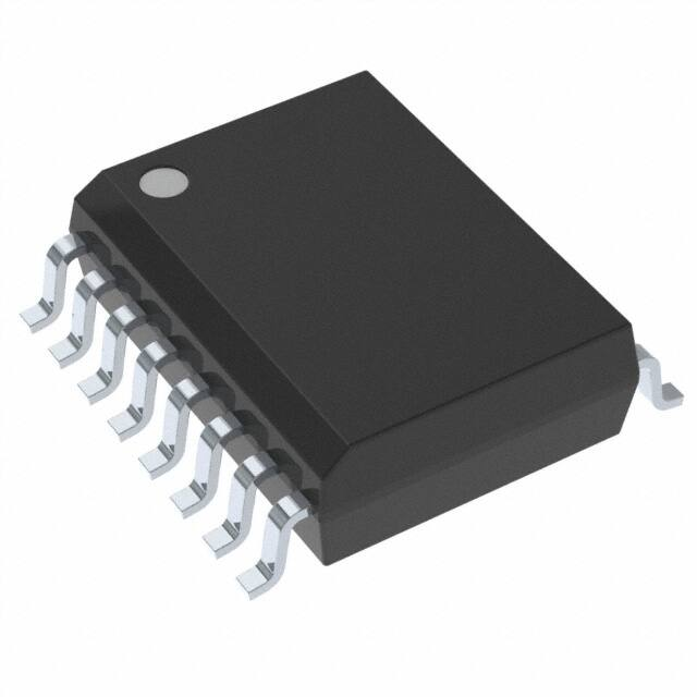


 工商网监
湘ICP备2023018690号
工商网监
湘ICP备2023018690号
