CY14V101Q3
1 Mbit (128 K × 8) Serial SPI nvSRAM
Features
■
1-Mbit nonvolatile static random access memory (nvSRAM)
❐ Internally organized as 128 K × 8
❐ STORE to QuantumTrap nonvolatile elements initiated
automatically on power-down (AutoStore) or by user using
HSB pin (Hardware STORE) or SPI instruction (Software
STORE)
❐ RECALL to SRAM initiated on power-up
(Power-Up RECALL) or by SPI instruction
(Software RECALL)
❐ Automatic STORE on power-down with a small capacitor
■
High reliability
❐ Infinite read, write, and RECALL cycles
❐ 1 million STORE cycles to QuantumTrap
❐ Data retention: 20 years
■
High speed serial peripheral interface (SPI)
❐ 30 MHz clock rate
❐ Supports SPI mode 0 (0,0) and mode 3 (1,1)
■
Write protection
❐ Hardware protection using Write Protect (WP) pin
❐ Software protection using Write Disable instruction
❐ Software block protection for 1/4,1/2, or entire array
■
Low power consumption
❐ Core VCC = 3.0 V to 3.6 V; I/O VCCQ = 1.65 V to 1.95 V
❐ Average active current of 10 mA at 30 MHz operation
■
Industry standard configurations
❐ Industrial temperature
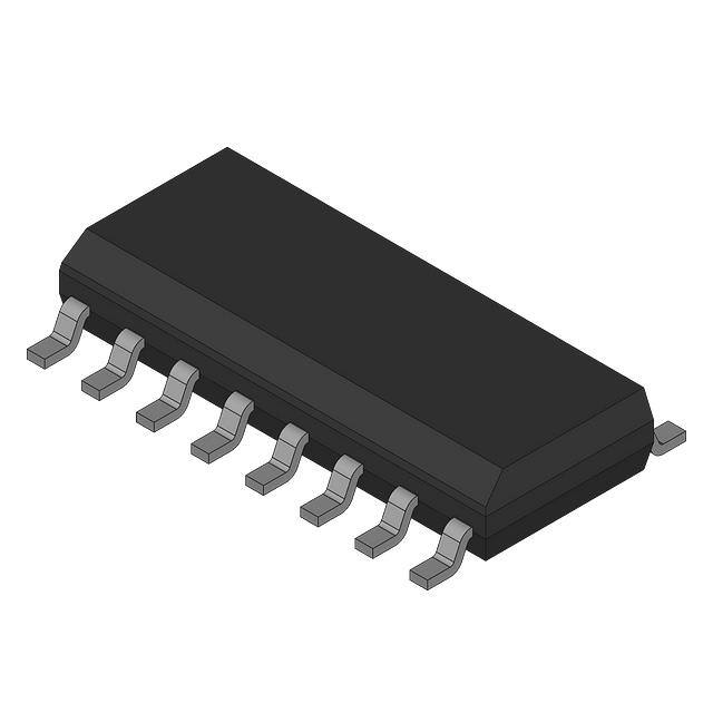
❐ 16-pin small outline integrated circuit (SOIC) package
❐ Restriction of hazardous substances (RoHS) compliant
Functional Overview
The Cypress CY14V101Q3 combines a 1 Mbit nvSRAM with a
nonvolatile element in each memory cell with serial SPI interface.
The memory is organized as 128 K words of 8 bits each. The
embedded nonvolatile elements incorporate the QuantumTrap
technology, creating the world’s most reliable nonvolatile
memory. The SRAM provides infinite read and write cycles, while
the QuantumTrap cell provides highly reliable nonvolatile
storage of data. Data transfers from SRAM to the nonvolatile
elements (STORE operation) takes place automatically at
power-down. On power-up, data is restored to the SRAM from
the nonvolatile memory (RECALL operation). Both STORE and
RECALL operations can also be initiated by the user through SPI
instruction.
For a complete list of related documentation, click here.
VCC VCCQ VCAP
Logic Block Diagram
CS
WP
SCK
Quantum Trap
128 K X 8
Instruction decode
Write protect
Control logic
STORE
SRAM ARRAY
HOLD
RECALL
128 K X 8
Instruction
register
Power Control
STORE/RECALL
Control
HSB
D0-D7
A0-A16
Address
Decoder
SI
Data I/O register
SO
Status register
Cypress Semiconductor Corporation
Document #: 001-67191 Rev. *E
•
198 Champion Court
•
San Jose, CA 95134-1709
•
408-943-2600
Revised November 13, 2014
�CY14V101Q3
Contents
Pinouts .............................................................................. 3
Device Operation .............................................................. 4
SRAM Write ................................................................. 4
SRAM Read ................................................................ 4
STORE Operation ....................................................... 4
AutoStore Operation .................................................... 5
Software STORE Operation ........................................ 5
Hardware STORE and HSB Pin Operation ................. 5
RECALL Operation ...................................................... 5
Hardware RECALL (Power-Up) .................................. 5
Software RECALL ....................................................... 5
Disabling and Enabling AutoStore ............................... 5
Noise Considerations ....................................................... 6
Serial Peripheral Interface ............................................... 6
SPI Overview ............................................................... 6
SPI Modes ................................................................... 7
SPI Operating Features.................................................... 8
Power-Up .................................................................... 8
Power On Reset .......................................................... 8
Power-Down ................................................................ 8
Active Power and Standby Power Modes ................... 8
SPI Functional Description .............................................. 8
Status Register ................................................................. 9
Read Status Register (RDSR) Instruction ................... 9
Write Status Register (WRSR) Instruction .................. 9
Write Protection and Block Protection ......................... 10
Write Enable (WREN) Instruction .............................. 10
Write Disable (WRDI) Instruction .............................. 10
Block Protection ........................................................ 10
Write Protect (WP) Pin .............................................. 11
Document #: 001-67191 Rev. *E
Memory Access .............................................................. 11
Read Sequence (READ) instruction .......................... 11
Write Sequence (WRITE) instruction ........................ 11
Software STORE (STORE) instruction ...................... 13
Software RECALL (RECALL) instruction .................. 13
AutoStore Enable (ASENB) instruction ..................... 13
AutoStore Disable (ASDISB) instruction ................... 13
HOLD Pin Operation ................................................. 14
Best Practices ................................................................. 14
Maximum Ratings ........................................................... 15
DC Electrical Characteristics ........................................ 15
Data Retention and Endurance ..................................... 16
Capacitance .................................................................... 16
Thermal Resistance ........................................................ 16
AC Test Conditions ........................................................ 16
AC Switching Characteristics ....................................... 17
AutoStore or Power-Up RECALL .................................. 18
Software Controlled STORE and RECALL Cycles ...... 19
Hardware STORE Cycle ................................................. 20
Ordering Information ...................................................... 21
Ordering Code Definition ........................................... 21
Package Diagrams .......................................................... 22
Acronyms ........................................................................ 23
Document Conventions ................................................. 23
Units of Measure ....................................................... 23
Document History Page ................................................ 24
Sales, Solutions, and Legal Information ...................... 24
Worldwide Sales and Design Support ....................... 24
Products .................................................................... 24
PSoC Solutions ......................................................... 24
Page 2 of 24
�CY14V101Q3
Pinouts
Figure 1. Pin Diagram – 16-pin SOIC
NC
1
16
VCC
NC
2
15
VCCQ
NC
3
14
VCAP
13
SO
12
SI
SCK
CY14V101Q3
NC
4
WP
5
HOLD
6
11
7
10
8
9
NC
VSS
Top View
not to scale
CS
HSB
Table 1. Pin Definitions
Pin Name
I/O Type
Description
CS
Input
Chip select. Activates the device when pulled LOW. Driving this pin high puts the device in low
power standby mode.
SCK
Input
Serial clock. Runs at speeds up to maximum of fSCK. Serial input is latched at the rising edge of
this clock. Serial output is driven at the falling edge of the clock.
SI
Input
Serial input. Pin for input of all SPI instructions and data.
SO
Output
WP
Input
Write protect. Implements hardware write protection in SPI.
HOLD
Input
HOLD pin. suspends serial operation.
HSB
Input/Output
Output: Indicates busy status of nvSRAM when LOW. After each Hardware and Software STORE
operation HSB is driven HIGH for a short time (tHHHD) with standard output high current and then
a weak internal pull-up resistor keeps this pin HIGH (External pull-up resistor connection optional).
Input: Hardware STORE implemented by pulling this pin LOW externally.
VCAP
Power supply
AutoStore capacitor. Supplies power to the nvSRAM during power loss to STORE data from the
SRAM to nonvolatile elements. If AutoStore is not needed, this pin must be left as No connect. It
must never be connected to VSS.
NC
No connect
VSS
Power supply
Ground
VCC
Power supply
Power supply (3.0 V to 3.6 V)
VCCQ
Power Supply
Power supply inputs for the inputs and outputs of the device.
Document #: 001-67191 Rev. *E
Serial output. Pin for output of data through SPI.
No connect: This pin is not connected to the die.
Page 3 of 24
�CY14V101Q3
Device Operation
CY14V101Q3 is a 1 Mbit nvSRAM memory with a nonvolatile
element in each memory cell. All the reads and writes to
nvSRAM happen to the SRAM which gives nvSRAM the unique
capability to handle infinite writes to the memory. The data in
SRAM is secured by a STORE sequence which transfers the
data in parallel to the nonvolatile QuantumTrap cells. A small
capacitor (VCAP) is used to AutoStore the SRAM data in
nonvolatile cells when power goes down providing power-down
data security. The QuantumTrap nonvolatile elements built in the
reliable SONOS technology make nvSRAM the ideal choice for
secure data storage.
The 1 Mbit memory array is organized as 128 K words x 8 bits.
The memory is accessed through a standard SPI interface that
enables very high clock speeds up to 30 MHz with zero cycle
delay read and write cycles. This device supports SPI modes 0
and 3 (CPOL, CPHA = 0, 0 and 1, 1) and operates as SPI slave.
The device is enabled using the Chip Select (CS) pin and
accessed through Serial Input (SI), Serial Output (SO), and
Serial Clock (SCK) pins.
This device provides the feature for hardware and software write
protection through the WP pin and WRDI instruction respectively
along with mechanisms for block write protection (1/4, 1/2, or full
array) using BP0 and BP1 pins in the status register. Further, the
HOLD pin can be used to suspend any serial communication
without resetting the serial sequence.
CY14V101Q3 uses the standard SPI opcodes for memory
access. In addition to the general SPI instructions for read and
write, it provides four special instructions which enable access to
four nvSRAM specific functions: STORE, RECALL, AutoStore
Disable (ASDISB), and AutoStore Enable (ASENB).
The major benefit of serial (SPI) nvSRAM over serial EEPROMs
is that all reads and writes to nvSRAM are performed at the
speed of SPI bus with zero cycle delay. Therefore, no wait time
is required after any of the memory accesses. The STORE and
RECALL operations need finite time to complete and all memory
accesses are inhibited during this time. While a STORE or
RECALL operation is in progress, the busy status of the device
is indicated by the Hardware STORE Busy (HSB) pin and also
reflected on the RDY bit of the Status Register.
SRAM Write
All writes to nvSRAM are carried out on the SRAM and do not
use up any endurance cycles of the nonvolatile memory. This
enables the user to perform infinite write operations. A write cycle
is performed through the WRITE instruction. The WRITE
instruction is issued through the SI pin of the nvSRAM and
Document #: 001-67191 Rev. *E
consists of the WRITE opcode, three bytes of address, and one
byte of data. Write to nvSRAM is done at SPI bus speed with zero
cycle delay.
The device allows burst mode writes to be performed through
SPI. This enables write operations on consecutive addresses
without issuing a new WRITE instruction. When the last address
in memory is reached in burst mode, the address rolls over to
0x0000 and the device continues to write.
The SPI write cycle sequence is defined in the memory access
section of SPI Protocol Description.
SRAM Read
A read cycle is performed at the SPI bus speed and the data is
read out with zero cycle delay after the READ instruction is
executed. The READ instruction is issued through the SI pin of
the nvSRAM and consists of the READ opcode and 3 bytes of
address. The data is read out on the SO pin.
This device allows burst mode reads to be performed through
SPI. This enables reads on consecutive addresses without
issuing a new READ instruction. When the last address in
memory is reached in burst mode read, the address rolls over to
0x0000 and the device continues to read.
The SPI read cycle sequence is defined in the memory access
section of SPI Protocol Description.
STORE Operation
STORE operation transfers the data from the SRAM to the
nonvolatile QuantumTrap cells. The device stores data to the
nonvolatile cells using one of the three STORE operations:
AutoStore, activated on device power-down; Software STORE,
activated by a STORE instruction; and Hardware STORE,
activated by the HSB. During the STORE cycle, an erase of the
previous nonvolatile data is first performed, followed by a
program of the nonvolatile elements. After a STORE cycle is
initiated, read/write to CY14V101Q3 is inhibited until the cycle is
completed.
The HSB signal or the RDY bit in the Status register can be
monitored by the system to detect if a STORE or Software
RECALL cycle is in progress. The busy status of nvSRAM is
indicated by HSB being pulled LOW or RDY bit being set to ‘1’.
To avoid unnecessary nonvolatile STOREs, AutoStore and
Hardware STORE operations are ignored unless at least one
write operation has taken place since the most recent STORE or
RECALL cycle. However, software initiated STORE cycles are
performed regardless of whether a write operation has taken
place.
Page 4 of 24
�CY14V101Q3
AutoStore Operation
Hardware STORE and HSB Pin Operation
The AutoStore operation is a unique feature of nvSRAM which
automatically stores the SRAM data to QuantumTrap during
power-down. This STORE makes use of an external capacitor
(VCAP) and enables the device to safely STORE the data in the
nonvolatile memory when power goes down.
The HSB pin in CY14V101Q3 is used to control and
acknowledge STORE operations. If no STORE or RECALL is in
progress, this pin can be used to request a Hardware STORE
cycle. When the HSB pin is driven LOW, nvSRAM conditionally
initiates a STORE operation after tDELAY duration. An actual
STORE cycle starts only if a write to the SRAM has been
performed since the last STORE or RECALL cycle. Reads and
writes to the memory are inhibited for tSTORE duration or as long
as HSB pin is LOW.
During normal operation, the device draws current from VCC to
charge the capacitor connected to the VCAP pin. When the
voltage on the VCC pin drops below VSWITCH during power-down,
the device inhibits all memory accesses to nvSRAM and
automatically performs a conditional STORE operation using the
charge from the VCAP capacitor. The AutoStore operation is not
initiated if no write cycle has been performed since the last
RECALL.
Note If a capacitor is not connected to VCAP pin, AutoStore must
be disabled by issuing the AutoStore Disable instruction
specified in AutoStore Disable (ASDISB) instruction on page 13.
If AutoStore is enabled without a capacitor on the VCAP pin, the
device attempts an AutoStore operation without sufficient charge
to complete the STORE. This corrupts the data stored in the
nvSRAM and Status register. To resume normal functionality, the
WRSR instruction must be issued to update the nonvolatile bits
BP0, BP1 and WPEN in the Status Register.
Figure 2 shows the proper connection of the storage capacitor
(VCAP) for AutoStore operation. See DC Electrical Characteristics on page 15 for the size of the VCAP.
Figure 2. AutoStore Mode
VCCQ
0.1uF
10kOhm
Note After each Hardware and Software STORE operation HSB
is driven HIGH for a short time (tHHHD) with standard output high
current and then remains HIGH by an internal 100 k pull-up
resistor.
Note For successful last data byte STORE, a hardware store
should be initiated at least one clock cycle after the last data bit
D0 is received.
Upon completion of the STORE operation, the nvSRAM memory
access is inhibited for tLZHSB time after HSB pin returns HIGH.
The HSB pin must be left unconnected if not used.
RECALL Operation
A RECALL operation transfers the data stored in the nonvolatile
QuantumTrap elements to the SRAM. A RECALL may be
initiated in two ways: Hardware RECALL, initiated on power-up;
and Software RECALL, initiated by a SPI RECALL instruction.
VCC
0.1uF
VCCQ
The HSB pin also acts as an open drain driver (internal 100 k
weak pull-up resistor) that is internally driven LOW to indicate a
busy condition when the STORE (initiated by any means) is in
progress.
Internally, RECALL is a two-step procedure. First, the SRAM
data is cleared. Next, the nonvolatile information is transferred
into the SRAM cells. All memory accesses are inhibited while a
RECALL cycle is in progress. The RECALL operation does not
alter the data in the nonvolatile elements.
VCC
Hardware RECALL (Power-up)
CS
VCAP
VCAP
VSS
During power-up, when VCC crosses VSWITCH, an automatic
RECALL sequence is initiated which transfers the content of
nonvolatile memory on to the SRAM. The data would previously
have been stored on the nonvolatile memory through a STORE
sequence.
A Power-up RECALL cycle takes tFA time to complete and the
memory access is disabled during this time. HSB pin is used to
detect the Ready status of the device.
Software STORE Operation
Software RECALL
Software STORE enables the user to trigger a STORE operation
through a special SPI instruction. STORE operation is initiated
by executing STORE instruction irrespective of whether a write
has been performed since the last NV operation.
Software RECALL enables the user to initiate a RECALL
operation to restore the content of nonvolatile memory on to the
SRAM. A Software RECALL is issued by using the SPI
instruction for RECALL.
A STORE cycle takes tSTORE time to complete, during which all
the memory accesses to nvSRAM are inhibited. The RDY bit of
the Status register or the HSB pin may be polled to find the
Ready or Busy status of the nvSRAM. After the tSTORE cycle time
is completed, the SRAM is activated again for read and write
operations.
A Software RECALL takes tRECALL time to complete during
which all memory accesses to nvSRAM are inhibited. The
controller must provide sufficient delay for the RECALL operation
to complete before issuing any memory access instructions.
Document #: 001-67191 Rev. *E
Page 5 of 24
�CY14V101Q3
Disabling and Enabling AutoStore
If the application does not require the AutoStore feature, it can
be disabled by using the ASDISB instruction. If this is done, the
nvSRAM does not perform a STORE operation at power-down.
AutoStore can be re-enabled by using the ASENB instruction.
However, these operations are not nonvolatile and if the user
need this setting to survive the power cycle, a STORE operation
must be performed following AutoStore Disable or Enable
operation.
Note CY14V101Q3 has AutoStore Enabled from the factory. If
AutoStore is disabled and VCAP is not required, then the VCAP
pin must be left open. VCAP pin must never be connected to
ground. Power-up RECALL operation cannot be disabled in any
case.
Noise Considerations
SPI Slave
The SPI slave device is activated by the master through the chip
select line. A slave device gets the SCK as an input from the SPI
master and all the communication is synchronized with this
clock. SPI slave never initiates a communication on the SPI bus
and acts on the instruction from the master.
CY14V101Q3 operates as a SPI slave and may share the SPI
bus with other SPI slave devices.
Chip Select (CS)
For selecting any slave device, the master needs to pull-down
the corresponding CS pin. Any instruction can be issued to a
slave device only while the CS pin is LOW. When the device is
not selected, data through the SI pin is ignored and the serial
output pin (SO) remains in a high-impedance state.
See CY application note AN1064.
Note A new instruction must begin with the falling edge of CS.
Therefore, only one opcode can be issued for each active chip
select cycle.
Serial Peripheral Interface
Serial Clock (SCK)
SPI Overview
Serial clock is generated by the SPI master and the
communication is synchronized with this clock after CS goes
LOW.
The SPI is a four-pin interface with Chip Select (CS), Serial Input
(SI), Serial Output (SO), and Serial Clock (SCK) pins.
CY14V101Q3 provides serial access to nvSRAM through SPI
interface. The SPI bus on this device can run at speeds up to
30 MHz.
The SPI is a synchronous serial interface which uses clock and
data pins for memory access and supports multiple devices on
the data bus. A device on SPI bus is activated using a CS pin.
The relationship between chip select, clock, and data is dictated
by the SPI mode. This device supports SPI modes 0 and 3. In
both these modes, data is clocked into the nvSRAM on the rising
edge of SCK starting from the first rising edge after CS goes
active.
The SPI protocol is controlled by opcodes. These opcodes
specify the commands from the bus master to the slave device.
After CS is activated the first byte transferred from the bus
master is the opcode. Following the opcode, any addresses and
data are then transferred. The CS must go inactive after an
operation is complete and before a new opcode can be issued.
The commonly used terms used in SPI protocol are as follows:
SPI Master
The SPI master device controls the operations on a SPI bus. A
SPI bus may have only one master with one or more slave
devices. All the slaves share the same SPI bus lines and the
master may select any of the slave devices using the CS pin. All
the operations must be initiated by the master activating a slave
device by pulling the CS pin of the slave LOW. The master also
generates the SCK and all the data transmission on SI and SO
lines are synchronized with this clock.
Document #: 001-67191 Rev. *E
CY14V101Q3 enables SPI modes 0 and 3 for data
communication. In both these modes, the inputs are latched by
the slave device on the rising edge of SCK and outputs are
issued on the falling edge. Therefore, the first rising edge of SCK
signifies the arrival of the first bit (MSB) of SPI instruction on the
SI pin. Further, all data inputs and outputs are synchronized with
SCK.
Data Transmission - SI and SO
SPI data bus consists of two lines, SI and SO, for serial data
communication. The SI is also referred to as Master Out Slave
In (MOSI) and SO is referred to as Master In Slave Out (MISO).
The master issues instructions to the slave through the SI pin,
while the slave responds through the SO pin. Multiple slave
devices may share the SI and SO lines as described earlier.
Most Significant Bit (MSB)
The SPI protocol requires that the first bit to be transmitted is the
most significant bit (MSB). This is valid for both address and data
transmission.
The 1 Mbit serial nvSRAM requires a 3-byte address for any read
or write operation. However, since the actual address is only
17 bits, it implies that the first seven bits which are fed in are
ignored by the device. Although these seven bits are ‘don’t care’,
Cypress recommends that these bits are treated as 0s to enable
seamless transition to higher memory densities.
Serial Opcode
After the slave device is selected with CS going LOW, the first
byte received is treated as the opcode for the intended operation.
CY14V101Q3 uses the standard opcodes for memory accesses.
In addition to the memory accesses, it provides additional
opcodes for the nvSRAM specific functions: STORE, RECALL,
AutoStore Enable, and AutoStore Disable. See Table 2 on page
8 for details.
Page 6 of 24
�CY14V101Q3
Invalid Opcode
Status Register
If an invalid opcode is received, the opcode is ignored and the
CY14V101Q3 has an 8-bit status register. The bits in the status
device ignores any additional serial data on the SI pin till the next
register are used to configure the SPI bus. These bits are
falling edge of CS and the SO pin remains tristated.
described in the Table 4 on page 9.
Figure 3. System Configuration Using SPI nvSRAM
SCK
M OSI
M IS O
SCK
SI
SO
SCK
SI
SO
u C o n tro lle r
C Y14V 101Q x
CS
C Y14V 101Q x
HO LD
CS
HO LD
CS1
HO LD 1
CS2
HO LD 2
SPI Modes
CY14V101Q3 may be driven by a microcontroller with its SPI
peripheral running in either of the following two modes:
■
SPI Mode 0 (CPOL=0, CPHA=0)
■
SPI Mode 3 (CPOL=1, CPHA=1)
The two SPI modes are shown in Figure 4 and Figure 5. The
status of clock when the bus master is in standby mode and not
transferring data is:
■
SCK remains at 0 for Mode 0
■
SCK remains at 1 for Mode 3
For both these modes, the input data is latched-in on the rising
edge of SCK starting from the first rising edge after CS goes
active. If the clock starts from a HIGH state (in mode 3), the first
rising edge, after the clock toggles, is considered. The output
data is available on the falling edge of SCK.
CPOL and CPHA bits must be set in the SPI controller for the
either Mode 0 or Mode 3. The device detects the SPI mode from
the status of SCK pin when the device is selected by bringing the
CS pin LOW. If SCK pin is LOW when the device is selected, SPI
Mode 0 is assumed and if SCK pin is HIGH, it works in SPI
Mode 3.
Figure 4. SPI Mode 0
Figure 5. SPI Mode 3
CS
CS
0
1
2
3
4
5
6
1
2
3
4
5
6
7
SCK
SCK
SI
0
7
7
6
5
4
MSB
Document #: 001-67191 Rev. *E
3
2
1
0
LSB
SI
7
MSB
6
5
4
3
2
1
0
LSB
Page 7 of 24
�CY14V101Q3
SPI Operating Features
Power-up
Power-up is defined as the condition when the power supply is
turned on and VCC crosses Vswitch voltage. During this time, the
CS must be allowed to follow the VCC voltage. Therefore, CS
must be connected to VCC through a suitable pull-up resistor. As
a built-in safety feature, CS is both edge sensitive and level
sensitive. After power-up, the device is not selected until a falling
edge is detected on CS. This ensures that CS is HIGH, before
going LOW to start the first operation.
As described earlier, nvSRAM performs a Power-up RECALL
operation after power-up and therefore, all memory accesses are
disabled for tFA duration after power-up. The HSB pin can be
probed to check the ready or busy status of nvSRAM after
power-up.
Power-on Reset
A power-on reset (POR) circuit is included to prevent inadvertent
writes. At power-up, the device does not respond to any
instruction until the VCC reaches the POR threshold voltage
(VSWITCH). After VCC transitions the POR threshold, the device
is internally reset and performs an Power-Up RECALL operation.
During Power-Up RECALL all device accesses are inhibited.
The device is in the following state after POR:
■
Deselected (after power-up, a falling edge is required on CS
before any instructions are started).
■
Standby power mode
■
Not in the HOLD condition
Status register state:
❐ Write Enable (WEN) bit is reset to 0.
❐ WPEN, BP1, BP0 unchanged from previous STORE
operation
❐ Don’t care bits 4-6 are reset to 0.
The WPEN, BP1, and BP0 bits of the Status Register are
nonvolatile bits and remain unchanged from the previous
STORE operation.
■
Before selecting and issuing instructions to the memory, a valid
and stable VCC voltage must be applied. This voltage must
remain valid until the end of the instruction transmission.
Power-Down
At power-down (continuous decay of VCC), when VCC drops from
the normal operating voltage and below the VSWITCH threshold
voltage, the device stops responding to any instruction sent to it.
If a write cycle is in progress and the last data bit D0 has been
received when the power goes down, it is allowed tDELAY time to
complete the write. After which all memory accesses are
inhibited and a conditional AutoStore operation is performed
(AutoStore is not performed if no writes have happened since
last RECALL cycle). When VCCQ < VIODIS, I/Os are disabled (no
STORE takes place). This protects against inadvertent writes
during brown out conditions on VCCQ supply.
However, to completely avoid the possibility of inadvertent writes
during power-down, ensure that the device is deselected and is
Document #: 001-67191 Rev. *E
in standby power mode, and the CS follows the voltage applied
on VCC.
Active Power and Standby Power Modes
When CS is LOW, the device is selected, and is in the active
power mode. The device consumes ICC current, as specified in
DC Electrical Characteristics on page 15. When CS is HIGH, the
device is deselected and the device goes into the standby power
mode if a STORE or RECALL cycle is not in progress. If a
STORE or RECALL cycle is in progress, the device goes into the
standby power mode after the STORE or RECALL cycle is
completed. In the standby power mode, the current drawn by the
device drops to ISB.
SPI Functional Description
The CY14V101Q3 uses an 8-bit instruction register. Instructions
and their operation codes are listed in Table 2. All instructions,
addresses, and data are transferred with the MSB first and start
with a HIGH to LOW CS transition. There are, in all, 10 SPI
instructions which provide access to most of the functions in
nvSRAM. Further, the WP, HOLD, and HSB pins provide
additional functionality driven through hardware.
Table 2. Instruction Set
Instruction
Category
Status Register
Control Instructions
SRAM
Read/Write
Instructions
Special NV
Instructions
Reserved
Instruction
Name
Opcode
Operation
WREN
0000 0110
Set write enable
latch
WRDI
0000 0100
Reset write
enable latch
RDSR
0000 0101
Read Status
Register
WRSR
0000 0001
Write Status
Register
READ
0000 0011
Read data from
memory array
WRITE
0000 0010
Write data to
memory array
STORE
0011 1100 Software STORE
RECALL
0110 0000
Software
RECALL
ASENB
0101 1001 AutoStore Enable
ASDISB
0001 1001 AutoStore Disable
- Reserved - 0001 1110
The SPI instructions are divided based on their functionality in
the following types:
❐ Status Register access: RDSR and WRSR instructions
❐ Write protection functions: WREN and WRDI instructions
along with WP pin and WEN, BP0, and BP1 bits
❐ SRAM memory access: READ and WRITE instructions
❐ nvSRAM special instructions: STORE, RECALL, ASENB,
and ASDISB
Page 8 of 24
�CY14V101Q3
Status Register
The status register bits are listed in Table 4. The status register consists of a Ready bit (RDY) and data protection bits BP1, BP0,
WEN, and WPEN. The RDY bit can be polled to check the Ready or Busy status while a nvSRAM STORE or Software RECALL cycle
is in progress. The status register can be modified by WRSR instruction and read by RDSR instruction. However, only the WPEN,
BP1, and BP0 bits of the Status Register can be modified by using WRSR instruction. The WRSR instruction has no effect on WEN
and RDY bits. The default value shipped from the factory for WEN, BP0, BP1, bits 4-6 and WPEN bits is ‘0’.
Table 3. Status Register Format
Bit 7
Bit 6
Bit 5
Bit 4
Bit 3
Bit 2
Bit 1
Bit 0
WPEN (0)
X (0)
X (0)
X (0)
BP1 (0)
BP0 (0)
WEN (0)
RDY
Table 4. Status Register Bit Definition
Definition
Description
Bit 0 (RDY)
Bit
Ready
Read only bit indicates the ready status of device to perform a memory access. This bit is
set to ‘1’ by the device while a STORE or Software RECALL cycle is in progress.
Bit 1 (WEN)
Write Enable
WEN indicates if the device is Write Enabled. This bit defaults to ‘0’ (disabled) on power-up.
WEN = '1' --> Write Enabled
WEN = '0' --> Write Disabled
Bit 2 (BP0)
Block protect bit ‘0’
Bit 3 (BP1)
Block protect bit ‘1’
Bits 4-6
Bit 7 (WPEN)
Used for block protection. For details see Table 5 on page 10.
Used for block protection. For details see Table 5 on page 10.
Don’t care
Bits are writable and volatile. On power-up, bits are written with ‘0’.
Write protect enable bit Used for enabling the function of Write Protect Pin (WP). For details see Table 6 on page 11.
Read Status Register (RDSR) Instruction
to select one of four levels of block protection. Further, WPEN bit
must be set to ‘1’ to enable the use of write protect (WP) pin.
The Read Status Register instruction provides access to the
status register. This instruction is used to probe the Write Enable
Status of the device or the Ready status of the device. RDY bit
is set by the device to ‘1’ whenever a STORE or Software
RECALL cycle is in progress. The block protection and WPEN
bits indicate the extent of protection employed.
WRSR instruction is a write instruction and needs writes to be
enabled (WEN bit set to ‘1’) using the WREN instruction before
it is issued. The instruction is issued after the falling edge of CS
using the opcode for WRSR followed by 8 bits of data to be
stored in the Status Register. Since only bits 2, 3, and 7 can be
modified by WRSR instruction; therefore, it is recommended to
leave the bits 4-6 as ‘0’ while writing to the Status Register
This instruction is issued after the falling edge of CS using the
opcode for RDSR.
Note In CY14V101Q3, the values written to Status Register are
saved to nonvolatile memory only after a STORE operation. If
AutoStore is disabled, any modifications to the Status Register
must be secured by performing a Software STORE operation.
Write Status Register (WRSR) Instruction
The WRSR instruction enables the user to write to the Status
register. However, this instruction cannot be used to modify bit 0
and bit 1 (RDY and WEN). The BP0 and BP1 bits can be used
Figure 6. Read Status Register (RDSR) Instruction Timing
CS
0
1
2
3
4
5
6
7
0
1
0
MSB
1
2
3
4
5
6
7
SCK
SI
SO
0
0
0
0
HI-Z
0
1
0
D7 D6 D5 D4 D3 D2 D1 D0
MSB
Document #: 001-67191 Rev. *E
LSB
Data
LSB
Page 9 of 24
�CY14V101Q3
Figure 7. Write Status Register (WRSR) Instruction Timing
CS
0
1
2
3
4
5
6
7
0
1
2
3
4
5
6
7
SCK
Data in
Opcode
SI
0
0
0
0
0
0
0
1 D7 X
MSB
X
X D3 D2 X
X
LSB
HI-Z
SO
Write Protection and Block Protection
Write Disable (WRDI) Instruction
CY14V101Q3 provides features for both software and hardware
write protection using WRDI instruction and WP. Additionally, this
device also provides block protection mechanism through BP0
and BP1 pins of the Status Register.
Write Disable instruction disables the write by clearing the WEN
bit to ‘0’ in order to protect the device against inadvertent writes.
This instruction is issued following the falling edge of CS followed
by opcode for WRDI instruction. The WEN bit is cleared on the
rising edge of CS following a WRDI instruction.
Figure 9. WRDI Instruction
The write enable and disable status of the device is indicated by
WEN bit of the status register. The write instructions (WRSR and
WRITE) and nvSRAM special instruction (STORE, RECALL,
ASENB, and ASDISB) need the write to be enabled (WEN bit =
1) before they can be issued.
Write Enable (WREN) Instruction
Note After completion of a write instruction (WRSR or WRITE)
or nvSRAM special instruction (STORE, RECALL, ASENB, and
ASDISB) instruction, WEN bit is cleared to ‘0’. This is done to
provide protection from any inadvertent writes. Therefore,
WREN instruction must be used before a new write instruction is
issued.
Figure 8. WREN Instruction
CS
1
2
3
4
5
6
7
SCK
SI
SO
0
0
0
0
0
HI-Z
Document #: 001-67191 Rev. *E
1
0
1
2
3
4
5
6
7
SCK
On power-up, the device is always in the write disable state. The
following WRITE, WRSR, or nvSRAM special instruction must
therefore be preceded by a Write Enable instruction. If the device
is not write enabled (WEN = ‘0’), it ignores the write instructions
and returns to the standby state when CS is brought HIGH. A
new CS falling edge is required to re-initiate serial
communication. The instruction is issued following the falling
edge of CS. When this instruction is used, the WEN bit of status
register is set to ‘1’. WEN bit defaults to ‘0’ on power-up.
0
CS
1
0
SI
0
0
0
0
0
1
0
0
HI-Z
SO
Block Protection
Block protection is provided using the BP0 and BP1 pins of the
Status register. These bits can be set using WRSR instruction
and probed using the RDSR instruction. The nvSRAM is divided
into four array segments. One-quarter, one-half, or all of the
memory segments can be protected. Any data within the
protected segment is read only. Table 5 shows the function of
block protect bits.
Table 5. Block Write Protect Bits
Level
Status Register
Bits
BP1
Array Addresses Protected
BP0
0
0
0
None
1 (1/4)
0
1
0x18000-0x1FFFF
2 (1/2)
1
0
0x10000-0x1FFFF
3 (All)
1
1
0x00000-0x1FFFF
Page 10 of 24
�CY14V101Q3
Write Protect (WP) Pin
and other bits as ‘don’t cares’. Address bits A15 to A0 are sent
in the following two address bytes. After the last address bit is
transmitted on the SI pin, the data (D7-D0) at the specific
address is shifted out on the SO line on the falling edge of SCK
starting with D7. Any other data on SI line after the last address
bit is ignored.
The write protect pin (WP) is used to provide hardware write
protection. WP pin enables all normal read and write operations
when held HIGH. When the WP pin is brought LOW and WPEN
bit is ‘1’, all write operations to the status register are inhibited.
The hardware write protection function is blocked when the
WPEN bit is ‘0’. This enables the user to install the device in a
system with the WP pin tied to ground, and still write to the status
register.
CY14V101Q3 allows reads to be performed in bursts through
SPI which can be used to read consecutive addresses without
issuing a new READ instruction. If only one byte is to be read,
the CS line must be driven HIGH after one byte of data comes
out. However, the read sequence may be continued by holding
the CS line LOW and the address is automatically incremented
and data continues to shift out on SO pin. When the last data
memory address (0x1FFFF) is reached, the address rolls over to
0x0000 and the device continues to read.
WP pin can be used along with WPEN and block protect bits
(BP1 and BP0) of the status register to inhibit writes to memory.
When WP pin is LOW and WPEN is set to ‘1’, any modifications
to status register are disabled. Therefore, the memory is
protected by setting the BP0 and BP1 bits and the WP pin inhibits
any modification of the status register bits, providing hardware
write protection.
Write Sequence (WRITE) instruction
Note WP going LOW when CS is still LOW has no effect on any
of the ongoing write operations to the status register.
The write operations on this device are performed through the SI
pin. To perform a write operation, if the device is write disabled,
then the device must first be write enabled through the WREN
instruction. When the writes are enabled (WEN = ‘1’), WRITE
instruction is issued after the falling edge of CS. A WRITE
instruction constitutes transmitting the WRITE opcode on SI line
followed by 3 bytes of address and the data (D7-D0) which is to
be written. The Most Significant address byte contains A16 in bit
0 with other bits being ‘don’t cares’. Address bits A15 to A0 are
sent in the following two address bytes.
Table 6 summarizes all the protection features of this device
Table 6. Write Protection Operation
Unprotected
WEN Protected
Blocks
Blocks
Status
Register
WPEN
WP
X
X
0
Protected
Protected
0
X
1
Protected
Writable
Writable
1
LOW
1
Protected
Writable
Protected
1
HIGH
1
Protected
Writable
Writable
Protected
Read Sequence (READ) instruction
CY14V101Q3 enables writes to be performed in bursts through
SPI which can be used to write consecutive addresses without
issuing a new WRITE instruction. If only one byte is to be written,
the CS line must be driven HIGH after the D0 (LSB of data) is
transmitted. However, if more bytes are to be written, CS line
must be held LOW and address is incremented automatically.
The following bytes on the SI line are treated as data bytes and
written in the successive addresses. When the last data memory
address (0x1FFFF) is reached, the address rolls over to 0x0000
and the device continues to write. The WEN bit is reset to ‘0’ on
completion of a WRITE sequence.
The read operations on this device are performed by giving the
instruction on SI and reading the output on SO pin. The following
sequence needs to be followed for a read operation: After the CS
line is pulled LOW to select a device, the read opcode is
transmitted through the SI line followed by three bytes of
address. The Most Significant address byte contains A16 in bit 0
Note When a burst write reaches a protected block address, it
continues the address increment into the protected space but
does not write any data to the protected memory. If the address
roll over takes the burst write to unprotected space, it resumes
writes. The same operation is true if a burst write is initiated
within a write protected block.
Memory Access
All memory accesses are done using the READ and WRITE
instructions. These instructions cannot be used while a STORE
or RECALL cycle is in progress. A STORE cycle in progress is
indicated by the RDY bit of the status register and the HSB pin.
Figure 10. Read Instruction Timing
CS
1
2
3
4
5
6
7
0
1
2
3
4
5
Op-Code
SI
0
0
0
0
0
SO
0
6
7
~
~ ~
~
0
SCK
20 21 22 23 0
1
2
3
4
5
6
7
17-bit Address
1
1
0 0
MSB
0
0
0
0
0 A16
A3 A2 A1 A0
LSB
D7 D6 D5 D4 D3 D2 D1 D0
LSB
Data
MSB
Document #: 001-67191 Rev. *E
Page 11 of 24
�CY14V101Q3
Figure 11. Burst Mode Read Instruction Timing
CS
2
3
4
5
6
7
0
1
2
3
4
5
6
7
Op-Code
0
0
0
0
1
2
3
4
5
6
7
0
0
7
1
2
3
4
5
6
7
17-bit Address
0
1
0
1
0
0
0
0
0
0
~
~
SI
20 21 22 23 0
~
~
1
~
~
0
SCK
A16
0
MSB
A3 A2 A1 A0
LSB
Data Byte N
~
~
Data Byte 1
SO
D7 D6 D5 D4 D3 D2 D1 D0 D7 D0 D7 D6 D5 D4 D3 D2 D1 D0
MSB
MSB
LSB
LSB
Figure 12. Write Instruction Timing
CS
1
2
3
4
5
0
7
6
1
2
3
4
5
6
7
~
~ ~
~
0
SCK
Op-Code
SI
0
0
0
0
0
20 21
22 23
0
1
2
3
4
5
6
7
17-bit Address
0
1
0
0
0
0
0
0
0
0
A16
MSB
A3 A2 A1 A0 D7 D6 D5 D4 D3 D2 D1 D0
LSB MSB
LSB
Data
HI-Z
SO
Figure 13. Burst Mode Write Instruction Timing
CS
2
3
4
5
6
7
0
1
2
3
4
5
6
7
20 21 22 23 0
1
2
3
4
5
6
7
0
0
0
17-bit Address
0
1
0
0
0
0
0
0
0
0
~
~
SI
0
A16
Document #: 001-67191 Rev. *E
2
3
4
5
6
7
A3 A2 A1 A0 D7 D6 D5 D4 D3 D2 D1 D0 D7 D0 D7 D6 D5 D4 D3 D2 D1 D0
LSB MSB
MSB
SO
1
~
~
Op-Code
0
0
Data Byte N
Data Byte 1
0
7
~
~
1
~
~
0
SCK
LSB
HI-Z
Page 12 of 24
�CY14V101Q3
nvSRAM Special Instructions
AutoStore Enable (ASENB) instruction
CY14V101Q3 provides four special instructions which enables
access to the nvSRAM specific functions: STORE, RECALL,
ASDISB, and ASENB. Table 7 lists these instructions.
The AutoStore Enable instruction enables the AutoStore on
CY14V101Q3. This setting is not nonvolatile and needs to be
followed by a STORE sequence if this is desired to survive the
power cycle.
Table 7. nvSRAM Special Instructions
Function Name
STORE
RECALL
ASENB
ASDISB
Opcode
0011 1100
0110 0000
0101 1001
0001 1001
Operation
Software STORE
Software RECALL
AutoStore Enable
AutoStore Disable
Software STORE (STORE) instruction
When a STORE instruction is executed, nvSRAM performs a
Software STORE operation. The STORE operation is performed
irrespective of whether a write has taken place since the last
STORE or RECALL operation.
To issue this instruction, the device must be write enabled (WEN
bit = ‘1’). The instruction is performed by transmitting the STORE
opcode on the SI pin following the falling edge of CS. The WEN
bit is cleared on the positive edge of CS following the STORE
instruction.
Figure 14. Software STORE Operation
To issue this instruction, the device must be write enabled (WEN
= ‘1’). The instruction is performed by transmitting the ASENB
opcode on the SI pin following the falling edge of CS. The WEN
bit is cleared on the positive edge of CS following the ASENB
instruction.
Note If ASDISB and ASENB instructions are executed in
CY14V101Q3, the device is busy for the duration of software
sequence processing time (tSS).
Figure 16. AutoStore Enable Operation
CS
0
1
2
3
4
5
6
7
SCK
SI
0
1
0
1
1
0
0
1
HI-Z
SO
CS
0
1
2
3
4
5
6
7
SCK
SI
0
0
1
1
1
1
0
0
HI-Z
SO
Software RECALL (RECALL) instruction
When a RECALL instruction is executed, nvSRAM performs a
Software RECALL operation. To issue this instruction, the device
must be write enabled (WEN = ‘1’).
The instruction is performed by transmitting the RECALL opcode
on the SI pin following the falling edge of CS. The WEN bit is
cleared on the positive edge of CS following the RECALL
instruction.
Figure 15. Software RECALL Operation
CS
0
1
2
3
4
5
6
7
AutoStore Disable (ASDISB) instruction
AutoStore is enabled by default in CY14V101Q3. The ASDISB
instruction disables the AutoStore. This setting is not nonvolatile
and needs to be followed by a STORE sequence if this is desired
to survive the power cycle.
To issue this instruction, the device must be write enabled (WEN
= ‘1’). The instruction is performed by transmitting the ASDISB
opcode on the SI pin following the falling edge of CS. The WEN
bit is cleared on the positive edge of CS following the ASDISB
instruction.
Figure 17. AutoStore Disable Operation
CS
0
1
2
3
4
5
6
7
SCK
SI
SO
0
0
0
1
1
0
0
1
HI-Z
SCK
SI
SO
0
1
1
0
0
0
0
0
HI-Z
Document #: 001-67191 Rev. *E
Page 13 of 24
�CY14V101Q3
Best Practices
HOLD Pin Operation
The HOLD pin is used to pause the serial communication. When
the device is selected and a serial sequence is underway, HOLD
is used to pause the serial communication with the master device
without resetting the ongoing serial sequence. To pause, the
HOLD pin must be brought LOW when the SCK pin is LOW. CS
pin must remain LOW along with HOLD pin to pause serial
communication. While the device serial communication is
paused, inputs to the SI pin are ignored and the SO pin is in the
high impedance state. To resume serial communication, the
HOLD pin must be brought HIGH when the SCK pin is LOW
(SCK may toggle during HOLD).
nvSRAM products have been used effectively for over 27 years.
While ease-of-use is one of the product’s main system values,
experience gained working with hundreds of applications has
resulted in the following suggestions as best practices:
■
The nonvolatile cells in this nvSRAM product are delivered from
Cypress with 0x00 written in all cells. Incoming inspection
routines at customer or contract manufacturer’s sites
sometimes reprogram these values. Final NV patterns are
typically repeating patterns of AA, 55, 00, FF, A5, or 5A. End
product’s firmware should not assume an NV array is in a set
programmed state. Routines that check memory content
values to determine first time system configuration, cold or
warm boot status, and so on should always program a unique
NV pattern (that is, complex 4-byte pattern of 46 E6 49 53 hex
or more random bytes) as part of the final system
manufacturing test to ensure these system routines work
consistently.
■
Power-up boot firmware routines should rewrite the nvSRAM
into the desired state (for example, AutoStore Enabled). While
the nvSRAM is shipped in a preset state, best practice is to
again rewrite the nvSRAM into the desired state as a safeguard
against events that might flip the bit inadvertently such as
program bugs and incoming inspection routines.
■
The VCAP value specified in this data sheet includes a minimum
and a maximum value size. Best practice is to meet this
requirement and not exceed the maximum VCAP value because
the nvSRAM internal algorithm calculates VCAP charge and
discharge time based on this maximum VCAP value. Customers
that want to use a larger VCAP value to make sure there is extra
STORE charge and STORE time should discuss their VCAP
size selection with Cypress to understand any impact on the
VCAP voltage level at the end of a tRECALL period.
Figure 18. HOLD Operation
SCK
~
~
CS
HOLD
SO
Document #: 001-67191 Rev. *E
Page 14 of 24
�CY14V101Q3
Maximum Ratings
Exceeding maximum ratings may shorten the useful life of the
device. These user guidelines are not tested.
Transient voltage ( 2001 V
(per MIL-STD-883, Method 3015)
Latch up current..................................................... > 140 mA
Operating Range
Input voltage ......................................–0.5 V to VCCQ + 0.5 V
Range
Ambient
Temperature
VCC
VCCQ
Industrial –40 C to +85 C 3.0 V to 3.6 V 1.65 V to 1.95 V
DC Electrical Characteristics
Over the Operating Range
Parameter
VCC
Description
Test Conditions
Power supply voltage
VCCQ
ICC1
ICCQ1
Average Vcc current
At fSCK = 30 MHz.
Average VCCQ current Values obtained without output loads (IOUT = 0 mA)
Min
Typ[1]
Max
Unit
3.0
3.3
3.6
V
1.65
1.8
1.95
V
–
–
10
mA
–
–
3
mA
–
–
10
mA
ICC2
Average VCC current
during STORE
ICC4
Average VCAP current All inputs don’t care. Average current for duration tSTORE
during AutoStore
cycle
–
–
5
mA
ISB
VCC standby current
–
–
5
mA
IIX[2]
Input leakage current VCCQ = Max, VSS < VIN < VCCQ
(except HSB)
–1
–
+1
µA
Input leakage current VCCQ = Max, VSS < VIN < VCCQ
(for HSB)
–100
–
+1
µA
–1
–
+1
µA
All inputs don’t care, VCC = Max.
Average current for duration tSTORE
CS > (VCCQ – 0.2 V). VIN < 0.2 V or > (VCCQ – 0.2 V).
Standby current level after nonvolatile cycle is complete.
Inputs are static. f = 0 MHz.
IOZ
Off state output
leakage current
VCCQ = Max, VSS < VOUT < VCCQ
VIH
Input HIGH voltage
0.7VCCQ
–
VCCQ +
0.3
V
VIL
Input LOW voltage
– 0.3
–
0.3 VCCQ
V
VOH
Output HIGH voltage IOUT = –1 mA
VCCQ –
0.45
–
–
V
VOL
Output LOW voltage
IOUT = 2 mA
–
–
0.45
V
VCAP[3]
Storage capacitor
Between VCAP pin and VSS, 5 V rated
61
68
180
µF
Notes
1. Typical values are at 25 °C, VCC= VCC (Typ) and VCCQ= VCCQ (Typ) . Not 100% tested.
2. The HSB pin has IOUT = -4 uA for VOH of 1.07V when both active HIGH and LOW drivers are disabled. When they are enabled standard VOH and VOL are valid. This
parameter is characterized but not tested.
3. Min VCAP value guarantees that there is a sufficient charge available to complete a successful AutoStore operation. Max VCAP value guarantees that the capacitor on
VCAP is charged to a minimum voltage during a Power-Up RECALL cycle so that an immediate power-down cycle can complete a successful AutoStore. Therefore it
is always recommended to use a capacitor within the specified min and max limits. See application note AN43593 for more details on VCAP options.
Document #: 001-67191 Rev. *E
Page 15 of 24
�CY14V101Q3
Data Retention and Endurance
Over the Operating Range
Parameter
Description
DATAR
Data retention
NVC
Nonvolatile STORE operations
Min
Unit
20
Years
1,000
K
Max
Unit
6
pF
8
pF
Capacitance
Parameter[4]
Description
Test Conditions
CIN
Input capacitance
COUT
Output pin capacitance
TA = 25 C, f = 1 MHz,
VCC = VCC (Typ), VCCQ = VCCQ (Typ)
Thermal Resistance
Parameter [4]
Description
JA
Thermal resistance
(junction to ambient)
JC
Thermal resistance
(junction to case)
Test Conditions
16-SOIC
Unit
55.17
C/W
2.64
C/W
Test conditions follow standard test methods
and procedures for measuring thermal
impedance, per EIA / JESD51.
Figure 19. AC Test Loads and Waveforms
450
450
1.8 V
1.8 V
R1
R1
OUTPUT
OUTPUT
30 pF
R2
450
5 pF
R2
450
AC Test Conditions
Input pulse levels.................................................0 V to 1.8 V
Input rise and fall times (10% - 90%).........................


 工商网监
湘ICP备2023018690号
工商网监
湘ICP备2023018690号
