Please note that Cypress is an Infineon Technologies Company.
The document following this cover page is marked as “Cypress” document as this is the
company that originally developed the product. Please note that Infineon will continue
to offer the product to new and existing customers as part of the Infineon product
portfolio.
Continuity of document content
The fact that Infineon offers the following product as part of the Infineon product
portfolio does not lead to any changes to this document. Future revisions will occur
when appropriate, and any changes will be set out on the document history page.
Continuity of ordering part numbers
Infineon continues to support existing part numbers. Please continue to use the
ordering part numbers listed in the datasheet for ordering.
www.infineon.com
�CY14V116N
16-Mbit (1024K × 16) nvSRAM
CY14V116N, 16-Mbit (1024K × 16) nvSRAM
Features
16-Mbit nonvolatile static random access memory (nvSRAM)
❐ 30-ns and 45-ns access times
❐ Logically organized as 1024K × 16
❐ Hands-off automatic STORE on power-down with only a
small capacitor
❐ STORE to QuantumTrap nonvolatile elements is initiated by
software, device pin, or AutoStore on power-down
❐ RECALL to SRAM initiated by software or power-up
■ High reliability
❐ Infinite read, write, and RECALL cycles
❐ 1 million STORE cycles to QuantumTrap
❐ Data retention: 20 years
■ Sleep mode operation
■ Low power consumption
❐ Active current of 75 mA at 45 ns
❐ Standby mode current of 650 µA
❐ Sleep mode current of 10 µA
■ Operating voltage
❐ Core VCC = 2.7 V to 3.6 V; I/O VCCQ = 1.65 V to 1.95 V
■
■
Industrial temperature: –40 C to +85 C
■
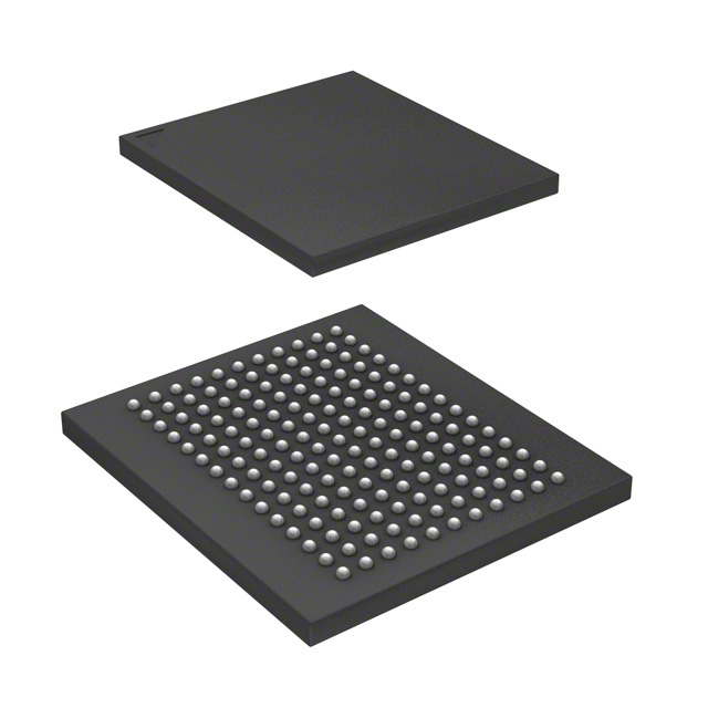
165-ball fine-pitch ball grid array (FBGA) package
■
Restriction of hazardous substances (RoHS) compliant
Functional Description
The Cypress CY14V116N is a fast SRAM, with a nonvolatile
element in each memory cell. The memory is organized as
1024K words of 16 bits each. The embedded nonvolatile
elements incorporate QuantumTrap technology, producing the
world’s most reliable nonvolatile memory. The SRAM can be
read and written an infinite number of times. The nonvolatile data
residing in the nonvolatile elements do not change when data is
written to the SRAM. Data transfers from the SRAM to the
nonvolatile elements (the STORE operation) takes place
automatically at power-down. On power-up, data is restored to
the SRAM (the RECALL operation) from the nonvolatile memory.
Both the STORE and RECALL operations are also available
under software control.
For a complete list of related documentation, click here.
V CC V CAP V CCQ
Logic Block Diagram
POWER CONTROL
SLEEP MODE
CONTROL
A 0-A11
ROW DECODER
QUANTUMTRAP
4096 X 4096
STORE
STORE / RECALL
CONTROL
ZZ
HSB
RECALL
STATIC RAM
ARRAY
4096 X 4096
SOFTWARE
DETECT
A 2-A14
OE
CE
CONTROL LOGIC
OUTPUT BUFFERS
COLUMN IO
SENSE AMPS
DQ 0-DQ 15
INPUT BUFFERS
WE
[1]
BLE
BHE
ZZ
COLUMN DECODER
A 12-A19
Note
1. In this datasheet, CE refers to the internal logical combination of CE1 and CE2, such that when CE1 is LOW and CE2 is HIGH, CE is LOW. For all other cases CE is HIGH.
Cypress Semiconductor Corporation
Document Number: 001-75791 Rev. *J
•
198 Champion Court
•
San Jose, CA 95134-1709
•
408-943-2600
Revised September 24, 2019
�CY14V116N
Contents
Pinout ................................................................................ 3
Pin Definitions .................................................................. 4
Device Operation .............................................................. 5
SRAM Read ................................................................ 5
SRAM Write ................................................................. 5
AutoStore Operation (Power-Down) ............................ 5
Hardware STORE (HSB) Operation ............................ 6
Hardware RECALL (Power-Up) .................................. 6
Software STORE ......................................................... 6
Software RECALL ....................................................... 6
Sleep Mode ................................................................. 8
Preventing AutoStore .................................................. 9
Data Protection ............................................................ 9
Maximum Ratings ........................................................... 10
Operating Range ............................................................. 10
DC Electrical Characteristics ........................................ 10
Data Retention and Endurance ..................................... 12
Capacitance .................................................................... 12
Thermal Resistance ........................................................ 12
AC Test Loads and Waveforms ..................................... 12
AC Test Conditions ........................................................ 12
Document Number: 001-75791 Rev. *J
AC Switching Characteristics ....................................... 13
AutoStore/Power-Up RECALL Characteristics ............ 17
Sleep Mode Characteristics ........................................... 19
Software Controlled STORE and RECALL
Characteristics ................................................................ 20
Hardware STORE Characteristics ................................. 22
Truth Table For SRAM Operations ................................ 23
Ordering Information ...................................................... 24
Ordering Code Definitions ......................................... 24
Package Diagram ............................................................ 25
Acronyms ........................................................................ 26
Document Conventions ............................................. 26
Units of Measure ....................................................... 26
Document History Page ................................................. 27
Sales, Solutions, and Legal Information ...................... 29
Worldwide Sales and Design Support ....................... 29
Products .................................................................... 29
PSoC® Solutions ...................................................... 29
Cypress Developer Community ................................. 29
Technical Support ..................................................... 29
Page 2 of 29
�CY14V116N
Pinout
Figure 1. Pin Diagram: 165-Ball FBGA (×16)
1
2
3
4
5
6
7
8
9
10
11
A
NC
A6
A8
WE
BLE
CE1
NC
OE
A5
A3
NC
B
NC
DQ0
DQ1
A4
BHE
CE2
NC
A2
NC
NC
NC
C
ZZ
NC
NC
VSS
A0
A7
A1
VSS
NC
DQ15
DQ14
D
NC
DQ2
NC
VSS
VSS
VSS
VSS
VSS
NC
NC
NC
E
NC
VCAP
NC
VCCQ
VSS
VSS
VSS
VCCQ
NC
DQ13
NC
F
NC
DQ3
NC
VCCQ
VCC
VSS
VCC
VCCQ
NC
NC
DQ12
G
HSB
NC
NC
VCCQ
VCC
VSS
VCC
VCCQ
NC
NC
NC
H
NC
NC
VCCQ
VCCQ
VCC
VSS
VCC
VCCQ
VCCQ
NC
NC
J
NC
NC
NC
VCCQ
VCC
VSS
VCC
VCCQ
NC
DQ8
NC
K
NC
NC
DQ4
VCCQ
VCC
VSS
VCC
VCCQ
NC
NC
NC
L
NC
DQ5
NC
VCCQ
VSS
VSS
VSS
VCCQ
NC
NC
DQ9
M
NC
NC
NC
VSS
VSS
VSS
VSS
VSS
NC
DQ10
NC
N
NC
DQ6
DQ7
VSS
A11
A10
A9
VSS
NC
NC
NC
P
NC
NC
NC
A13
A19
NC
A18
A12
NC
DQ11
NC
R
NC
NC
A15
NC
A17
NC
A16
NC[2]
A14
NC
NC
Note
2. Address expansion for 32-Mbit. NC pin not connected to die.
Document Number: 001-75791 Rev. *J
Page 3 of 29
�CY14V116N
Pin Definitions
Pin Name
I/O Type
A0–A19
Input
Description
Address inputs. Used to select one of the 1,048,576 words of the nvSRAM.
DQ0–DQ15 Input/Output Bidirectional data I/O lines. Used as input or output lines depending on operation.
WE
Input
Write Enable input, Active LOW. When selected LOW, data on the I/O pins is written to the specific
address location.
CE1, CE2
Input
Chip Enable input. The device is selected and a memory access begins on the falling edge of CE1
(while CE2 is HIGH) or the rising edge of CE2 (while CE1 is LOW).
OE
Input
Output Enable, Active LOW. The active LOW OE input enables the data output buffers during read
cycles. Deasserting OE HIGH causes the I/O pins to tristate.
BLE
Input
Byte Enable, Active LOW. When selected LOW, enables DQ7–DQ0.
BHE
Input
Byte Enable, Active LOW. When selected LOW, enables DQ15–DQ8.
ZZ
Input
Sleep Mode Enable. When the ZZ pin is pulled LOW, the device enters a low-power Sleep mode and
consumes the lowest power. Because this input is logically AND’ed with CE, ZZ must be HIGH for normal
operation.
VCC
VCCQ
VSS
Power supply Power. Power supply inputs to the core of the device.
Power supply I/O Power. Power supply inputs for the inputs and outputs of the device.
Power Supply Ground for the device. Must be connected to ground of the system.
HSB
Input/Output Hardware STORE Busy (HSB).When LOW, this output indicates that a Hardware STORE is in progress.
When pulled LOW external to the chip, it initiates a nonvolatile STORE operation. After each Hardware
and Software STORE operation, HSB is driven HIGH for a short time (tHHHD) with standard output high
current and then a weak internal pull-up resistor keeps this pin HIGH (external pull-up resistor connection
optional).
VCAP
Power Supply AutoStore capacitor. Supplies power to the nvSRAM during power loss to store data from SRAM to
nonvolatile elements.
NC
NC
No Connect. Die pads are not connected to the package pin.
Document Number: 001-75791 Rev. *J
Page 4 of 29
�CY14V116N
Device Operation
The CY14V116N nvSRAM is made up of two functional components paired in the same physical cell. These are an SRAM
memory cell and a nonvolatile QuantumTrap cell. The SRAM
memory cell operates as a standard fast static RAM. Data in the
SRAM is transferred to the nonvolatile cell (the STORE
operation) automatically at power-down, or from the nonvolatile
cell to the SRAM (the RECALL operation) on power-up. Both the
STORE and RECALL operations are also available under
software control. Using this unique architecture, all cells are
stored and recalled in parallel. During the STORE and RECALL
operations, SRAM read and write operations are inhibited. The
CY14V116N supports infinite reads and writes to the SRAM. In
addition, it provides infinite RECALL operations from the nonvolatile cells and up to 1 million STORE operations. See the Truth
Table For SRAM Operations on page 23 for a complete
description of read and write modes.
During normal operation, the device draws current from VCC to
charge a capacitor connected to the VCAP pin. This stored
charge is used by the chip to perform a STORE operation during
power-down. If the voltage on the VCC pin drops below VSWITCH,
the part automatically disconnects the VCAP pin from VCC and a
STORE operation is initiated with power provided by the VCAP
capacitor.
Note If the capacitor is not connected to the VCAP pin, AutoStore
must be disabled using the soft sequence specified in the section
Preventing AutoStore on page 9. If AutoStore is enabled without
a capacitor on the VCAP pin, the device attempts an AutoStore
operation without sufficient charge to complete the STORE. This
corrupts the data stored in the nvSRAM.
Figure 2. AutoStore Mode
VCCQ
VCC
SRAM Read
SRAM Write
A write cycle is performed when CE and WE are LOW and HSB
is HIGH. The address inputs must be stable before entering the
write cycle and must remain stable until CE or WE goes HIGH at
the end of the cycle. The data on the common I/O pins
DQ0–DQ15 is written into the memory if it is valid tSD before the
end of a WE-controlled write or before the end of a CE-controlled
write. The Byte Enable inputs (BHE, BLE) determine which bytes
are written. Keep OE HIGH during the entire write cycle to avoid
data bus contention on common I/O lines. If OE is left LOW, the
internal circuitry turns off the output buffers tHZWE after WE goes
LOW.
AutoStore Operation (Power-Down)
The CY14V116N stores data to the nonvolatile QuantumTrap
cells using one of the three storage operations. These three
operations are: Hardware STORE, activated by the HSB;
Software STORE, activated by an address sequence; AutoStore,
on device power-down. The AutoStore operation is a unique
feature of nvSRAM and is enabled by default on the CY14V116N
device.
Document Number: 001-75791 Rev. *J
0.1uF
0.1uF
10 k:
The CY14V116N performs a read cycle whenever CE and OE
are LOW, and WE, ZZ, and HSB are HIGH. The address
specified on pins A0–A19 determines which of the 1,048,576
words of 16 bits each are accessed. Byte enables (BHE, BLE)
determine which bytes are enabled to the output. When the read
is initiated by an address transition, the outputs are valid after a
delay of tAA (read cycle 1). If the read is initiated by CE or OE,
the outputs are valid at tACE or at tDOE, whichever is later (read
cycle 2). The data output repeatedly responds to address
changes within the tAA access time without the need for transitions on any control input pins. This remains valid until another
address change or until CE or OE is brought HIGH, or WE or
HSB is brought LOW.
VCCQ
VCC
WE
VCAP
VCAP
VSS
Figure 2 shows the proper connection of the storage capacitor
(VCAP) for automatic STORE operation. Refer to DC Electrical
Characteristics on page 10 for the size of the VCAP. The voltage
on the VCAP pin is driven to VVCAP by a regulator on the chip. A
pull-up resistor should be placed on WE to hold it inactive during
power-up. This pull-up resistor is only effective if the WE signal
is in tristate during power-up. When the nvSRAM comes out of
power-up-RECALL, the host microcontroller must be active or
the WE held inactive until the host microcontroller comes out of
reset.
To reduce unnecessary nonvolatile STOREs, AutoStore and
Hardware STORE operations are ignored unless at least one
write operation has taken place (which sets a write latch) since
the most recent STORE or RECALL cycle. Software initiated
STORE cycles are performed regardless of whether a write
operation has taken place.
Page 5 of 29
�CY14V116N
Hardware STORE (HSB) Operation
The CY14V116N provides the HSB pin to control and
acknowledge the STORE operations. The HSB pin is used to
request a Hardware STORE cycle. When the HSB pin is driven
LOW, the device conditionally initiates a STORE operation after
tDELAY. A STORE cycle begins only if a write to the SRAM has
taken place since the last STORE or RECALL cycle. The HSB
pin also acts as an open drain driver (an internal 100-k weak
pull-up resistor) that is internally driven LOW to indicate a busy
condition when the STORE (initiated by any means) is in
progress.
Note After each Hardware and Software STORE operation, HSB
is driven HIGH for a short time (tHHHD) with standard output high
current and then remains HIGH by an internal 100-k pull-up
resistor.
SRAM write operations that are in progress when HSB is driven
LOW by any means are given time (tDELAY) to complete before
the STORE operation is initiated. However, any SRAM write
cycles requested after HSB goes LOW are inhibited until HSB
returns HIGH. If the write latch is not set, HSB is not driven LOW
by the device. However, any of the SRAM read and write cycles
are inhibited until HSB is returned HIGH by the host microcontroller or another external source.
During any STORE operation, regardless of how it is initiated,
the device continues to drive the HSB pin LOW, releasing it only
when the STORE is complete. Upon completion of the STORE
operation, the nvSRAM memory access is inhibited for tLZHSB
time after the HSB pin returns HIGH. Leave the HSB unconnected if it is not used.
Hardware RECALL (Power-Up)
During power-up or after any low-power condition
(VCC < VSWITCH), an internal RECALL request is latched. When
VCC again exceeds the VSWITCH on power-up, a RECALL cycle
is automatically initiated and takes tHRECALL to complete. During
this time, the HSB pin is driven LOW by the HSB driver and all
reads and writes to nvSRAM are inhibited.
To initiate the Software STORE cycle, the following read
sequence must be performed:
1. Read address 0x4E38 Valid Read
2. Read address 0xB1C7 Valid Read
3. Read address 0x83E0 Valid Read
4. Read address 0x7C1F Valid Read
5. Read address 0x703F Valid Read
6. Read address 0x8FC0 Initiate STORE cycle
The software sequence may be clocked with CE-controlled
reads or OE-controlled reads, with WE kept HIGH for all the six
read sequences. After the sixth address in the sequence is
entered, the STORE cycle commences and the chip is disabled.
HSB is driven LOW. After the tSTORE cycle time is fulfilled, the
SRAM is activated again for the read and write operation.
Software RECALL
Data is transferred from the nonvolatile memory to the SRAM by
a software address sequence. A software RECALL cycle is
initiated with a sequence of read operations in a manner similar
to the Software STORE initiation.
To initiate the RECALL cycle, perform the following sequence of
CE or OE controlled read operations:
1. Read address 0x4E38 Valid Read
2. Read address 0xB1C7 Valid Read
3. Read address 0x83E0 Valid Read
4. Read address 0x7C1F Valid Read
5. Read address 0x703F Valid Read
6. Read address 0x4C63 Initiate RECALL cycle
Internally, RECALL is a two-step procedure. First, the SRAM
data is cleared; then, the nonvolatile information is transferred
into the SRAM cells. After the tRECALL cycle time, the SRAM is
again ready for read and write operations. The RECALL
operation does not alter the data in the nonvolatile elements.
Software STORE
Data is transferred from the SRAM to the nonvolatile memory by
a software address sequence. A Software STORE cycle is
initiated by executing sequential CE or OE controlled read cycles
from six specific address locations in exact order. During the
STORE cycle, the previous nonvolatile data is first erased,
followed by a store into the nonvolatile elements. After a STORE
cycle is initiated, further reads and writes are disabled until the
cycle is completed.
Because a sequence of reads from specific addresses is used
for STORE initiation, it is important that no other read or write
accesses intervene in the sequence. Otherwise, the sequence is
aborted and no STORE or RECALL takes place.
Document Number: 001-75791 Rev. *J
Page 6 of 29
�CY14V116N
Table 1. Mode Selection
CE[3]
H
WE
X
OE
X
BHE, BLE
X
A15–A0[4]
X
Mode
I/O
Power
Not selected
Output High Z
Standby
L
H
L
L
X
Read SRAM
Output Data
Active
L
L
X
L
X
Write SRAM
Input Data
Active
L
H
L
X
0x4E38
0xB1C7
0x83E0
0x7C1F
0x703F
0x8B45
Read SRAM
Read SRAM
Read SRAM
Read SRAM
Read SRAM
AutoStore
Disable
Output Data
Output Data
Output Data
Output Data
Output Data
Output Data
Active[5]
L
H
L
X
0x4E38
0xB1C7
0x83E0
0x7C1F
0x703F
0x4B46
Read SRAM
Read SRAM
Read SRAM
Read SRAM
Read SRAM
AutoStore
Enable
Output Data
Output Data
Output Data
Output Data
Output Data
Output Data
Active[5]
L
H
L
X
0x4E38
0xB1C7
0x83E0
0x7C1F
0x703F
0x8FC0
Read SRAM
Read SRAM
Read SRAM
Read SRAM
Read SRAM
Nonvolatile
STORE
Output Data
Output Data
Output Data
Output Data
Output Data
Output High Z
Active ICC2[5]
L
H
L
X
0x4E38
0xB1C7
0x83E0
0x7C1F
0x703F
0x4C63
Read SRAM
Read SRAM
Read SRAM
Read SRAM
Read SRAM
Nonvolatile
RECALL
Output Data
Output Data
Output Data
Output Data
Output Data
Output High Z
Active[5]
Notes
3. In this datasheet, CE refers to the internal logical combination of CE1 and CE2 such that when CE1 is LOW and CE2 is HIGH, CE is LOW. Intermediate voltage levels
are not permitted on any of the chip enable pins.
4. While there are 20 address lines on the CY14V116N, only 13 address lines (A14–A2) are used to control software modes. The remaining address lines are don’t care.
5. The six consecutive address locations must be in the order listed. WE must be HIGH during all six cycles to enable a nonvolatile operation.
Document Number: 001-75791 Rev. *J
Page 7 of 29
�CY14V116N
Sleep Mode
In Sleep mode, the device consumes the lowest power supply
current (IZZ). The device enters a low-power Sleep mode after
asserting the ZZ pin LOW. After the Sleep mode is registered,
the nvSRAM does a STORE operation to secure the data to the
nonvolatile memory and then enters the low-power mode. The
device starts consuming IZZ current after tSLEEP time from the
instance when the Sleep mode is initiated. When the ZZ pin is
LOW, all input pins are ignored except the ZZ pin. The nvSRAM
is not accessible for normal operations while it is in Sleep mode.
Note When nvSRAM enters the Sleep mode, it initiates a nonvolatile STORE cycle, which results in losing one endurance cycle
for every Sleep mode entry unless the data was not written to the
nvSRAM since the last nonvolatile STORE/RECALL operation.
When the ZZ pin is de-asserted (HIGH), there is a delay tWAKE
before you can access the device. If Sleep mode is not used, the
ZZ pin should be tied to VCCQ.
Figure 3. Sleep Mode (ZZ) Flow Diagram
Power Applied
After tHRECALL
After tWAKE
Device Ready
CE = LOW
ZZ = HIGH
CE = HIGH
ZZ = HIGH
CE = LOW; ZZ = HIGH
Active Mode
(ICC)
Standby Mode
(ISB)
CE = HIGH; ZZ = HIGH
CE = Don’t Care
ZZ = HIGH
ZZ = LOW
ZZ = LOW
Sleep Routine
After tSLEEP
Sleep Mode
(IZZ)
Document Number: 001-75791 Rev. *J
Page 8 of 29
�CY14V116N
Preventing AutoStore
Data Protection
The AutoStore function is disabled by initiating an AutoStore
disable sequence. A sequence of read operations is performed
in a manner similar to the Software STORE initiation.
The CY14V116N protects data from corruption during
low-voltage conditions by inhibiting all externally initiated
STORE and write operations. The low-voltage condition is
detected when VCC is less than VSWITCH. If the CY14V116N is
in a Write mode at power-up (both CE and WE are LOW), after
a RECALL or STORE, the write is inhibited until the SRAM is
enabled after tLZHSB (HSB to output active). When VCC < VIODIS,
I/Os are disabled (no STORE takes place). This protects against
inadvertent writes during power-up or brown out conditions.
To initiate the AutoStore disable sequence, the following
sequence of CE or OE controlled read operations must be
performed:
1. Read address 0x4E38 Valid Read
2. Read address 0xB1C7 Valid Read
3. Read address 0x83E0 Valid Read
4. Read address 0x7C1F Valid Read
5. Read address 0x703F Valid Read
6. Read address 0x8B45 AutoStore Disable
AutoStore is re-enabled by initiating an AutoStore enable
sequence. A sequence of read operations is performed in a
manner similar to the software RECALL initiation.
To initiate the AutoStore enable sequence, the following
sequence of CE or OE controlled read operations must be
performed:
1. Read address 0x4E38 Valid Read
2. Read address 0xB1C7 Valid Read
3. Read address 0x83E0 Valid Read
4. Read address 0x7C1F Valid Read
5. Read address 0x703F Valid Read
6. Read address 0x4B46 AutoStore Enable
If the AutoStore function is disabled or re-enabled, a manual
software STORE operation must be performed to save the
AutoStore state through subsequent power-down cycles. The
part comes from the factory with AutoStore enabled and 0x00
written in all cells.
Document Number: 001-75791 Rev. *J
Page 9 of 29
�CY14V116N
Maximum Ratings
Exceeding maximum ratings may impair the useful life of the
device. These user guidelines are not tested.
Storage temperature ................................ –65 C to +150 C
Maximum accumulated storage time
At 150 C ambient temperature ................................. 1000 h
At 85 C ambient temperature ................................ 20 Years
Maximum junction temperature ................................. 150 C
Supply voltage on VCC relative to VSS .........–0.5 V to +4.1 V
Supply voltage on VCCQ relative to VSS .....–0.5 V to +2.45 V
Voltage applied to outputs
in high-Z state ...................................–0.5 V to VCCQ + 0.5 V
Input voltage .....................................–0.5 V to VCCQ + 0.5 V
Transient voltage ( 2001 V
Latch-up current ................................................... > 140 mA
Operating Range
Ambient
VCC
VCCQ
Temperature (TA)
Industrial –40 C to +85 C 2.7 V to 3.6 V 1.65 V to 1.95 V
Range
DC Electrical Characteristics
Over the Operating Range
Parameter
Description
VCC
Core power supply
VCCQ
I/O power supply
ICC1
Average VCC current
ICCQ1
Average VCCQ current
Test Conditions
–
Min
Typ[6]
Max
Unit
2.7
3.0
3.6
V
1.65
1.80
1.95
V
Values obtained without tRC = 30 ns
output loads
tRC = 45 ns
(IOUT = 0 mA)
–
–
95
mA
–
–
75
mA
Values obtained without tRC = 30 ns
output loads
tRC = 45 ns
(IOUT = 0 mA)
–
–
30
mA
–
–
25
mA
ICC2
Average VCC current during
STORE
All inputs don’t care, VCC = VCC (max).
Average current for duration tSTORE
–
–
10
mA
ICC3
All inputs cycling at CMOS levels.
Average VCC current
at tRC = 200 ns, VCC (typ), 25 °C Values obtained without output loads
(IOUT = 0 mA).
–
50
–
mA
ICCQ3
Average VCC current
All inputs cycling at CMOS levels.
at tRC = 200 ns, VCCQ (typ), 25 °C Values obtained without output loads
(IOUT = 0 mA).
–
15
–
mA
ICC4[7]
Average VCAP current during
AutoStore cycle
–
–
6
mA
All inputs don’t care. Average current
for duration tSTORE
Notes
6. Typical values are at 25 °C, VCC = VCC (typ) and VCCQ = VCCQ (typ). Not 100% tested.
7. This parameter is only guaranteed by design and is not tested.
8. The HSB pin has IOUT = -4 µA for VOH of 1.07 V when both active HIGH and LOW drivers are disabled. When they are enabled standard VOH and VOL are valid. This
parameter is characterized but not tested.
9. Min VCAP value guarantees that there is a sufficient charge available to complete a successful AutoStore operation. Max VCAP value guarantees that the capacitor
on VCAP is charged to a minimum voltage during a Power-Up RECALL cycle so that an immediate power-down cycle can complete a successful AutoStore. Therefore,
it is always recommended to use a capacitor within the specified min and max limits.
10. Maximum voltage on VCAP pin (VVCAP) is provided for guidance when choosing the VCAP capacitor. The voltage rating of the VCAP capacitor across the operating
temperature range should be higher than the VVCAP voltage.
11. These parameters are only guaranteed by design and are not tested.
Document Number: 001-75791 Rev. *J
Page 10 of 29
�CY14V116N
DC Electrical Characteristics (continued)
Over the Operating Range
Parameter
ISB
Test Conditions
Min
Typ[6]
Max
Unit
CE > (VCCQ – 0.2 V).
tRC = 30 ns
VIN < 0.2 V or
tRC = 45 ns
> (VCCQ – 0.2 V).
Standby current level
after nonvolatile cycle is
complete. Inputs are
static. f = 0 MHz.
–
–
650
µA
–
–
500
µA
Description
VCC standby current
IZZ
Sleep mode current
All inputs are static at CMOS level
–
–
10
µA
IIX[8]
Input leakage current
(except HSB)
VCC = VCC (max), VSS < VIN < VCC
–1
–
+1
µA
Input leakage current
(for HSB)
VCC = VCC (max), VSS < VIN < VCC
–100
–
+1
µA
Off state output leakage current
VCC = VCC (max), VSS < VOUT < VCC,
–1
–
+1
µA
–
0.7 × VCCQ
–
VCCQ + 0.3
V
IOZ
CE or OE > VIH or BLE/BHE > VIH or
WE < VIL
VIH
Input HIGH voltage
VIL
Input LOW voltage
–
Vss – 0.3
–
0.3 × VCCQ
V
VOH
Output HIGH voltage
IOUT = –1 mA
VCCQ –
0.45
–
–
V
VOL
Output LOW voltage
IOUT = 2 mA
–
–
0.45
V
VCAP[9
VVCAP[10, 11]
Storage capacitor
Between VCAP pin and VSS
19.8
22.0
82.0
F
Maximum voltage driven on
VCAP pin by the device
VCC = VCC (max)
–
–
5.0
V
Notes
6. Typical values are at 25 °C, VCC = VCC (typ) and VCCQ = VCCQ (typ). Not 100% tested.
7. This parameter is only guaranteed by design and is not tested.
8. The HSB pin has IOUT = -4 µA for VOH of 1.07 V when both active HIGH and LOW drivers are disabled. When they are enabled standard VOH and VOL are valid. This
parameter is characterized but not tested.
9. Min VCAP value guarantees that there is a sufficient charge available to complete a successful AutoStore operation. Max VCAP value guarantees that the capacitor
on VCAP is charged to a minimum voltage during a Power-Up RECALL cycle so that an immediate power-down cycle can complete a successful AutoStore. Therefore,
it is always recommended to use a capacitor within the specified min and max limits.
10. Maximum voltage on VCAP pin (VVCAP) is provided for guidance when choosing the VCAP capacitor. The voltage rating of the VCAP capacitor across the operating
temperature range should be higher than the VVCAP voltage.
11. These parameters are only guaranteed by design and are not tested.
Document Number: 001-75791 Rev. *J
Page 11 of 29
�CY14V116N
Data Retention and Endurance
Over the Operating Range
Parameter
Description
DATAR
Data retention
NVC
Nonvolatile STORE operations
Min
Unit
20
Years
1,000,000
Cycles
Capacitance
In the following table, the capacitance parameters are listed.
Parameter [12]
Description
CIN
Input capacitance
CIO
Input/Output capacitance
COUT
Output capacitance
Test Conditions
TA = 25 C, f = 1 MHz,
VCC = VCC (typ), VCCQ = VCCQ (typ)
Max
Unit
10
pF
10
pF
10
pF
Thermal Resistance
In the following table, the thermal resistance parameters are listed.
Parameter [12]
Test Conditions
165-ball
FBGA
Unit
Test conditions follow standard test methods and
procedures for measuring thermal impedance, in
accordance with EIA/JESD51.
15.6
C/W
2.9
C/W
Description
JA
Thermal resistance
(junction to ambient)
JC
Thermal resistance
(junction to case)
AC Test Loads and Waveforms
Figure 4. AC Test Loads and Waveforms
For Tristate specs
13636
514
1.8 V
1.8 V
R1
R1
OUTPUT
OUTPUT
CL
30 pF
R2
720
CL
5 pF
R2
11538
AC Test Conditions
Input pulse levels ................................................0 V to 1.8 V
Input rise and fall times (10%–90%) ........................... < 3 ns
Input and output timing reference levels ....................... 0.9 V
Note
12. These parameters are only guaranteed by design and are not tested.
Document Number: 001-75791 Rev. *J
Page 12 of 29
�CY14V116N
AC Switching Characteristics
Over the Operating Range
Parameters [13]
Cypress
Parameter
30 ns
Description
Alt
Parameter
45 ns
Unit
Min
Max
Min
Max
30
–
45
ns
SRAM Read Cycle
tACE
tACS
Chip enable access time
–
[14]
tRC
Read cycle time
30
–
45
–
ns
tAA [15]
tAA
Address access time
–
30
–
45
ns
tDOE
tOE
Output enable to data valid
–
14
–
20
ns
tOHA[15]
tLZCE [16]
tHZCE [16, 17]
tLZOE [16]
tHZOE [16, 17]
tPU [16]
tPD [16]
tOH
Output hold after address change
3
–
3
–
ns
tLZ
Chip enable to output active
3
–
3
–
ns
tHZ
Chip disable to output inactive
–
12
–
15
ns
tOLZ
Output enable to output active
0
–
0
–
ns
tOHZ
Output disable to output inactive
–
12
–
15
ns
tPA
Chip enable to power active
0
–
0
–
ns
tPS
Chip disable to power standby
–
30
–
45
ns
tDBE
-
Byte enable to data valid
–
14
–
20
ns
tLZBE[16]
tHZBE[16, 17]
-
Byte enable to output active
0
–
0
–
ns
-
Byte disable to output inactive
–
12
–
15
ns
tRC
SRAM Write Cycle
tWC
tWC
Write cycle time
30
–
45
–
ns
tPWE
tWP
Write pulse width
24
–
30
–
ns
tSCE
tCW
Chip enable to end of write
24
–
30
–
ns
tSD
tDW
Data setup to end of write
14
–
15
–
ns
tHD
tDH
Data hold after end of write
0
–
0
–
ns
tAW
tAW
Address setup to end of write
24
–
30
–
ns
tSA
tAS
Address setup to start of write
0
–
0
–
ns
tHA
tWR
Address hold after end of write
0
–
0
–
ns
tHZWE
[16, 17, 18]
tWZ
Write enable to output disable
–
12
–
15
ns
tLZWE
[16]
tOW
Output active after end of write
3
–
3
–
ns
-
Byte enable to end of write
24
–
30
–
ns
tBW
Notes
13. Test conditions assume a signal transition time of 3 ns or less, timing reference levels of VCCQ/2, input pulse levels of 0 to VCCQ (typ), and output loading of the specified
IOL/IOH and 30-pF load capacitance, as shown in Figure 4 on page 12.
14. WE must be HIGH during SRAM read cycles.
15. Device is continuously selected with CE, OE and BLE, BHE LOW.
16. These parameters are only guaranteed by design and are not tested.
17. tHZCE, tHZOE, tHZBE, and tHZWE are specified with a load capacitance of 5 pF. Transition is measured ±200 mV from the steady state output voltage.
18. If WE is LOW when CE goes LOW, the outputs remain in the high impedance state.
Document Number: 001-75791 Rev. *J
Page 13 of 29
�CY14V116N
Figure 5. SRAM Read Cycle 1: Address Controlled[19, 20, 21]
tRC
Address
Address Valid
tAA
Data Output
Output Data Valid
Previous Data Valid
tOHA
Figure 6. SRAM Read Cycle 2: CE and OE Controlled[22, 23]
Address
Address Valid
tRC
[26]
tHZCE
tACE
CE
tAA
tLZCE
tHZOE
tDOE
OE
tHZBE
tLZOE
tDBE
BHE, BLE
tLZBE
Data Output
High Impedance
Output Data Valid
tPU
ICC
Standby
tPD
Active
Notes
19. WE must be HIGH during SRAM read cycles.
20. Device is continuously selected with CE, OE and BLE, BHE LOW.
21. HSB must remain HIGH during Read and Write cycles.
22. WE must be HIGH during SRAM read cycles.
23. HSB must remain HIGH during Read and Write cycles.
Document Number: 001-75791 Rev. *J
Page 14 of 29
�CY14V116N
Figure 7. SRAM Write Cycle 1: WE Controlled[27, 25, 28]
tWC
Address
Address Valid
tSCE
tHA
[26]
CE
tBW
BHE, BLE
tAW
tPWE
WE
tSA
tSD
Data Input
Input Data Valid
tHZWE
Data Output
tHD
Previous Data
tLZWE
High Impedance
Notes
24. WE must be HIGH during SRAM read cycles.
25. HSB must remain HIGH during Read and Write cycles.
26. In this datasheet CE refers to the internal logical combination of CE1 and CE2 such that when CE1 is LOW and CE2 is HIGH, CE is LOW. Intermediate voltage levels
are not permitted on any of the chip enable pins.
27. If WE is LOW when CE goes LOW, the outputs remain in the high impedance state.
28. CE or WE must be >VIH during address transitions.
Document Number: 001-75791 Rev. *J
Page 15 of 29
�CY14V116N
Figure 8. SRAM Write Cycle 2: CE Controlled[29, 30, 31]
tWC
Address Valid
Address
tSA
tSCE
tHA
[32]
CE
tBW
BHE, BLE
tPWE
WE
tHD
tSD
Data Input
Input Data Valid
High Impedance
Data Output
Figure 9. SRAM Write Cycle 3: BHE, BLE Controlled[29, 30, 31]
tWC
Address
Address Valid
tSCE
[32]
CE
tSA
tHA
tBW
BHE, BLE
tAW
tPWE
WE
tSD
Data Input
Data Output
tHD
Input Data Valid
High Impedance
Notes
29. If WE is LOW when CE goes LOW, the outputs remain in the high-impedance state.
30. HSB must remain HIGH during Read and Write cycles.
31. CE or WE must be >VIH during address transitions.
32. In this datasheet, CE refers to the internal logical combination of CE1 and CE2 such that when CE1 is LOW and CE2 is HIGH, CE is LOW. Intermediate voltage levels
are not permitted on any of the chip enable pins.
Document Number: 001-75791 Rev. *J
Page 16 of 29
�CY14V116N
AutoStore/Power-Up RECALL Characteristics
Over the Operating Range
Parameter
tHRECALL
[33]
tSTORE [34]
tDELAY
[35, 36]
VSWITCH
[36]
Description
Min
Max
Unit
Power-Up RECALL duration
–
30
ms
STORE cycle duration
–
8
ms
Time allowed to complete SRAM write cycle
–
25
ns
Low voltage trigger level
–
2.65
V
150
–
s
VIODIS[37]
I/O disable voltage on VCCQ
–
1.5
V
VHDIS[36]
tLZHSB[36]
tHHHD[36]
HSB output disable voltage
–
1.9
V
HSB to output active time
–
5
s
HSB HIGH active time
–
500
ns
tVCCRISE
VCC rise time
Notes
33. tHRECALL starts from the time VCC rises above VSWITCH.
34. If an SRAM write has not taken place since the last nonvolatile cycle, no AutoStore or Hardware STORE takes place.
35. On a Hardware STORE and AutoStore initiation, SRAM write operation continues to be enabled for time tDELAY.
36. These parameters are only guaranteed by design and are not tested.
37. HSB is not defined below VIODIS voltage.
Document Number: 001-75791 Rev. *J
Page 17 of 29
�CY14V116N
Figure 10. AutoStore or Power-Up RECALL[38]
VCC
VSWITCH
VIODIS
VCCQ
VIODIS
t VCCRISE
[39]
tHHHD
Note
Note
t HHHD
[40]
HSB out
VCCQ
[39]
tSTORE
tSTORE
Note
Note
[40]
tDELAY
tLZHSB
AutoStore
t LZHSB
tDELAY
Power-Up
RECALL
tHRECALL
tHRECALL
Read & Write
Inhibited
(RWI )
Power-Up
RECALL
Read & Write
Power-Up
RECALL
VCC
BROWN
OUT
AutoStore
Read
Read Power-down
AutoStore
&
&
Write V
Write
CCQ
BROWN
OUT
I/O Disable
Notes
38. Read and Write cycles are ignored during STORE, RECALL, and while VCC is below VSWITCH.
39. If an SRAM write has not taken place since the last nonvolatile cycle, no AutoStore or Hardware STORE takes place.
40. During power-up and power-down, HSB glitches when HSB pin is pulled up through an external resistor.
Document Number: 001-75791 Rev. *J
Page 18 of 29
�CY14V116N
Sleep Mode Characteristics
Over the Operating Range
Parameter
Description
Min
Max
Unit
tWAKE
Sleep mode exit time (ZZ HIGH to first access after wakeup)
–
30
ms
tSLEEP
Sleep mode enter time (ZZ LOW to CE don’t care)
–
8
ms
tZZL
ZZ active LOW time
50
–
ns
tWEZZ
Last write to Sleep mode entry time
0
–
s
tZZH
ZZ active to DQ Hi-Z time
–
70
ns
Figure 11. Sleep Mode [41]
V CC
V
SWITCH
V
SWITCH
t
t
SLEEP
HRECALL
t
WAKE
ZZ
t
WEZZ
WE
t
DQ
Read & Write
Inhibited
(RWI)
ZZH
Data
Power-Up
RECALL
Read & Write
Sleep
Entry
Sleep
Sleep
Exit
Read & Write
Power-down
AutoStore
Note
41. Device initiates sleep routine and enters into Sleep mode after tSLEEP duration.
Document Number: 001-75791 Rev. *J
Page 19 of 29
�CY14V116N
Software Controlled STORE and RECALL Characteristics
Over the Operating Range
Parameter [42, 43]
Description
30 ns
45 ns
Unit
Min
Max
Min
Max
30
–
45
–
ns
tRC
STORE/RECALL initiation cycle time
tSA
Address setup time
0
–
0
–
ns
tCW
Clock pulse width
24
–
30
–
ns
tHA
Address hold time
0
–
0
–
ns
RECALL duration
–
600
–
600
s
Soft sequence processing time
–
500
–
500
s
tRECALL
tSS
[44, 45]
Notes
42. The software sequence is clocked with CE controlled or OE controlled reads.
43. The six consecutive addresses must be read in the order listed in Table 1 on page 7. WE must be HIGH during all six consecutive cycles.
44. This is the amount of time it takes to take action on a soft sequence command. Vcc power must remain high to effectively register command.
45. Commands such as STORE and RECALL lock out I/O until the operation is complete which further increases this time. See the specific command.
Document Number: 001-75791 Rev. *J
Page 20 of 29
�CY14V116N
Figure 12. CE and OE Controlled Software STORE and RECALL Cycle[46]
tRC
Address
tRC
Address #1
tSA
[47]
Address #6
tCW
tCW
CE
tHA
tSA
tHA
tHA
tHA
OE
tHHHD
HSB (STORE only)
tHZCE
tLZCE
t DELAY
[48]
Note
tLZHSB
High Impedance
tSTORE/tRECALL
DQ (DATA)
RWI
Figure 13. AutoStore Enable and Disable Cycle
Address
tRC
tRC
Address #1
Address #6
tSA
[47]
CE
tCW
tCW
tHA
tSA
tHA
tHA
tHA
OE
tLZCE
tSS
tHZCE
Note
[48]
t DELAY
DQ (DATA)
RWI
Notes
46. The six consecutive addresses must be read in the order listed in Table 1 on page 7. WE must be HIGH during all six consecutive cycles.
47. In this datasheet, CE refers to the internal logical combination of CE1 and CE2 such that when CE1 is LOW and CE2 is HIGH, CE is LOW. Intermediate voltage levels
are not permitted on any of the chip enable pins.
48. DQ output data at the sixth read may be invalid because the output is disabled at tDELAY time.
Document Number: 001-75791 Rev. *J
Page 21 of 29
�CY14V116N
Hardware STORE Characteristics
Over the Operating Range
Parameter
Description
Min
Max
Unit
tDHSB
HSB to output active time when write latch not set
–
25
ns
tPHSB
Hardware STORE pulse width
15
–
ns
Figure 14. Hardware STORE Cycle[49]
Write Latch set
~
~
tPHSB
HSB (IN)
tSTORE
tHHHD
~
~
tDELAY
HSB (OUT)
tLZHSB
RWI
Write Latch not set
~
~
tPHSB
HSB (IN)
tDELAY
~
~
HSB (OUT)
HSB pin is driven HIGH to VCCQ only by internal
100 K: resistor, HSB driver is disabled
SRAM is disabled as long as HSB (IN) is driven LOW.
RWI
Figure 15. Soft Sequence Processing[50, 51]
Soft Sequence
Command
Address
[52]
Address #1
tSA
Address #6
tCW
tSS
Soft Sequence
Command
Address #1
tSS
Address #6
tCW
CE
V CC
Notes
49. If an SRAM write has not taken place since the last nonvolatile cycle, no AutoStore or Hardware STORE takes place.
50. This is the amount of time it takes to take action on a soft sequence command. Vcc power must remain high to effectively register command.
51. Commands, such as STORE and RECALL, lock out I/O until the operation is complete which further increases this time. See the specific command.
52. In this datasheet, CE refers to the internal logical combination of CE1 and CE2 such that when CE1 is LOW and CE2 is HIGH, CE is LOW. Intermediate voltage levels
are not permitted on any of the chip enable pins.
Document Number: 001-75791 Rev. *J
Page 22 of 29
�CY14V116N
Truth Table For SRAM Operations
HSB should remain HIGH for SRAM Operations.
CE1
CE2
WE
OE
BHE
BLE
H
X
X
X
X
X
High-Z
Deselect/Power-down
Standby
X
L
X
X
X
X
High-Z
Deselect/Power-down
Standby
L
H
X
X
H
H
High-Z
Output disabled
Active
L
H
H
L
L
L
Data out (DQ0–DQ15)
Read
Active
L
H
H
L
H
L
Data out (DQ0–DQ7);
DQ8–DQ15 in High-Z
Read
Active
L
H
H
L
L
H
Data out (DQ8–DQ15);
DQ0–DQ7 in High-Z
Read
Active
L
H
H
H
X
X
High-Z
Output disabled
Active
L
H
L
X
L
L
Data in (DQ0–DQ15)
Write
Active
L
H
L
X
H
L
Data in (DQ0–DQ7);
DQ8–DQ15 in High-Z
Write
Active
L
H
L
X
L
H
Data in (DQ8–DQ15);
DQ0–DQ7 in High-Z
Write
Active
Document Number: 001-75791 Rev. *J
Inputs and Outputs
Mode
Power
Page 23 of 29
�CY14V116N
Ordering Information
Speed (ns)
30
Ordering Code
Package Diagram
CY14V116N-BZ30XI
51-85195
Package Type
165-ball FBGA
Operating Range
Industrial
CY14V116N-BZ30XIT
All parts are Pb-free. Contact your local Cypress sales representative for availability of these parts.
Ordering Code Definitions
CY 14
V 116 N - BZ
30
X
I
T
Option: T = Tape and Reel; Blank = Std.
Temperature Grade: I = Industrial (40 oC to + 85 oC)
Pb-free
Speed: 30 = 30 ns; 45 = 45 ns
Package Type: BZ = 165-ball FBGA
Data Bus: N = x16
Density: 116 = 16-Mbit
Voltage: V = 3.0 VCC, 1.8 V VCCQ
14 = nvSRAM
Company ID: CY = Cypress
Document Number: 001-75791 Rev. *J
Page 24 of 29
�CY14V116N
Package Diagram
Figure 16. 165-ball FBGA (15 mm × 17 mm × 1.40 mm) Package Outline, 51-85195
51-85195 *D
Document Number: 001-75791 Rev. *J
Page 25 of 29
�CY14V116N
Acronyms
Document Conventions
Table 2. Acronyms Used in this Document
Units of Measure
Acronym
Description
Table 3. Units of Measure
CMOS
Complementary Metal Oxide Semiconductor
EIA
Electronic Industries Alliance
°C
degrees Celsius
FBGA
Fine-Pitch Ball Grid Array
Hz
hertz
I/O
Input/Output
Kbit
kilobit
JESD
JEDEC Standards
kHz
kilohertz
nvSRAM
nonvolatile Static Random Access Memory
k
kiloohm
RoHS
Restriction of Hazardous Substances
A
microampere
RWI
Read and Write Inhibited
mA
milliampere
F
microfarad
Mbit
megabit
MHz
megahertz
s
microsecond
ms
millisecond
ns
nanosecond
pF
picofarad
V
volt
ohm
W
watt
Document Number: 001-75791 Rev. *J
Symbol
Unit of Measure
Page 26 of 29
�CY14V116N
Document History Page
Document Title: CY14V116N, 16-Mbit (1024K × 16) nvSRAM
Document Number: 001-75791
Rev.
ECN No.
Submission
Date
Description of Change
**
3516347
02/03/2011
New data sheet.
*A
3733467
09/14/2012
Updated Device Operation:
Updated Sleep Mode:
Added Figure 3.
Updated Maximum Ratings:
Removed “Ambient temperature with power applied” and its details.
Added “Maximum junction temperature” and its details.
Updated DC Electrical Characteristics:
Added VVCAP parameter and its details.
Added Note 9 and referred the same note in VVCAP parameter.
Updated Capacitance:
Changed maximum value of CIN and COUT parameters from 7 pF to 11.5 pF.
Added Sleep Mode Characteristics.
*B
3944873
03/26/2013
Removed CY14W116N, CY14W116S, CY14V116S part related information in all instances across
the document.
Removed “VCC = 2.375 V to 2.625 V” operating range related information in all instances across
the document.
Removed 25 ns speed bin related information in all instances across the document.
Added 30 ns speed bin related information in all instances across the document.
Removed × 32 Configuration related information in all instances across the document.
Updated Features:
Replaced “I/O VCCQ = 1.65 V to VCC” with “I/O VCCQ = 1.65 V to 1.95 V”.
Updated DC Electrical Characteristics:
Updated details corresponding to VIH, VIL, VOL, VOH parameters.
Updated Capacitance (Changed maximum value of CIN and COUT parameters from 11.5 pF to 8
pF).
Updated AC Test Loads and Waveforms:
Updated Figure 4.
*C
4260504
01/24/2014
Updated Logic Block Diagram (for more clarity).
Updated Device Operation:
Updated AutoStore Operation (Power-Down):
Updated description (Removed “The HSB signal is monitored by the system to detect if an AutoStore cycle is in progress.”).
Updated Sleep Mode:
Updated Figure 3 (for more clarity).
Updated DC Electrical Characteristics:
Splitted ISB parameter to two rows.
Updated details in “Test Conditions” column corresponding to ISB parameter (Added “tRC = 30 ns”
and “tRC = 45 ns”).
Retained the existing values of ISB parameter for “tRC = 30 ns”.
Added values of ISB parameter for “tRC = 45 ns”.
Updated Note 8.
Changed minimum value of VCAP parameter from 20 F to 19.8 F.
Updated AC Switching Characteristics:
Updated Note 17.
Updated AutoStore/Power-Up RECALL Characteristics:
Updated Figure 10 (for more clarity).
Updated Sleep Mode Characteristics:
Changed maximum value of tZZH parameter from 20 ns to 70 ns.
Updated Figure 11 (for more clarity).
Completing Sunset Review.
*D
4417851
06/24/2014
Updated DC Electrical Characteristics:
Added Note 7 and referred the same note in ICC4 parameter.
Updated maximum value of VVCAP parameter from 4.5 V to 5.0 V.
Updated Capacitance:
Updated maximum value of CIN and COUT parameters from 8 pF to 10 pF.
Added CIO parameter and its details.
Updated Thermal Resistance:
Changed value of JA parameter from 22.0 C/W to 15.6 C/W corresponding to “165-ball FBGA”
package.
Changed value of JC parameter from 15.28 C/W to 2.9 C/W corresponding to “165-ball FBGA”
package.
Document Number: 001-75791 Rev. *J
Page 27 of 29
�CY14V116N
Document History Page
(continued)
Document Title: CY14V116N, 16-Mbit (1024K × 16) nvSRAM
Document Number: 001-75791
Rev.
ECN No.
Submission
Date
*E
4432183
07/07/2014
Description of Change
Updated DC Electrical Characteristics:
Changed maximum value of VCAP parameter from 120.0 F to 82.0 F.
*F
4456803
07/31/2014
No technical updates.
*G
4571551
11/17/2014
Updated Functional Description:
Added “For a complete list of related documentation, click here.” at the end.
*H
4616093
01/07/2015
Changed status from Preliminary to Final.
Completing Sunset Review.
*I
6093693
03/09/2018
Updated Package Diagram:
spec 51-85195 – Changed revision from *C to *D.
Updated to new template.
*J
6681289
09/24/2019
Updated Sales page and Copyright information.
Updated Ordering Information:
Removed CY14V116N-BZ45XI part number.
Added CY14V116N-BZ30XIT part number.
Document Number: 001-75791 Rev. *J
Page 28 of 29
�CY14V116N
Sales, Solutions, and Legal Information
Worldwide Sales and Design Support
Cypress maintains a worldwide network of offices, solution centers, manufacturer’s representatives, and distributors. To find the office
closest to you, visit us at Cypress Locations.
PSoC® Solutions
Products
Arm® Cortex® Microcontrollers
Automotive
cypress.com/arm
cypress.com/automotive
Clocks & Buffers
Interface
cypress.com/clocks
cypress.com/interface
Internet of Things
Memory
cypress.com/iot
cypress.com/memory
Microcontrollers
cypress.com/mcu
PSoC
cypress.com/psoc
Power Management ICs
Touch Sensing
USB Controllers
Wireless Connectivity
PSoC 1 | PSoC 3 | PSoC 4 | PSoC 5LP | PSoC 6 MCU
Cypress Developer Community
Community | Projects | Video | Blogs | Training | Components
Technical Support
cypress.com/support
cypress.com/pmic
cypress.com/touch
cypress.com/usb
cypress.com/wireless
© Cypress Semiconductor Corporation, 2011-2019. This document is the property of Cypress Semiconductor Corporation and its subsidiaries ("Cypress"). This document, including any software or
firmware included or referenced in this document ("Software"), is owned by Cypress under the intellectual property laws and treaties of the United States and other countries worldwide. Cypress reserves
all rights under such laws and treaties and does not, except as specifically stated in this paragraph, grant any license under its patents, copyrights, trademarks, or other intellectual property rights. If
the Software is not accompanied by a license agreement and you do not otherwise have a written agreement with Cypress governing the use of the Software, then Cypress hereby grants you a personal,
non-exclusive, nontransferable license (without the right to sublicense) (1) under its copyright rights in the Software (a) for Software provided in source code form, to modify and reproduce the Software
solely for use with Cypress hardware products, only internally within your organization, and (b) to distribute the Software in binary code form externally to end users (either directly or indirectly through
resellers and distributors), solely for use on Cypress hardware product units, and (2) under those claims of Cypress's patents that are infringed by the Software (as provided by Cypress, unmodified)
to make, use, distribute, and import the Software solely for use with Cypress hardware products. Any other use, reproduction, modification, translation, or compilation of the Software is prohibited.
TO THE EXTENT PERMITTED BY APPLICABLE LAW, CYPRESS MAKES NO WARRANTY OF ANY KIND, EXPRESS OR IMPLIED, WITH REGARD TO THIS DOCUMENT OR ANY SOFTWARE
OR ACCOMPANYING HARDWARE, INCLUDING, BUT NOT LIMITED TO, THE IMPLIED WARRANTIES OF MERCHANTABILITY AND FITNESS FOR A PARTICULAR PURPOSE. No computing
device can be absolutely secure. Therefore, despite security measures implemented in Cypress hardware or software products, Cypress shall have no liability arising out of any security breach, such
as unauthorized access to or use of a Cypress product. CYPRESS DOES NOT REPRESENT, WARRANT, OR GUARANTEE THAT CYPRESS PRODUCTS, OR SYSTEMS CREATED USING
CYPRESS PRODUCTS, WILL BE FREE FROM CORRUPTION, ATTACK, VIRUSES, INTERFERENCE, HACKING, DATA LOSS OR THEFT, OR OTHER SECURITY INTRUSION (collectively, "Security
Breach"). Cypress disclaims any liability relating to any Security Breach, and you shall and hereby do release Cypress from any claim, damage, or other liability arising from any Security Breach. In
addition, the products described in these materials may contain design defects or errors known as errata which may cause the product to deviate from published specifications. To the extent permitted
by applicable law, Cypress reserves the right to make changes to this document without further notice. Cypress does not assume any liability arising out of the application or use of any product or
circuit described in this document. Any information provided in this document, including any sample design information or programming code, is provided only for reference purposes. It is the responsibility
of the user of this document to properly design, program, and test the functionality and safety of any application made of this information and any resulting product. "High-Risk Device" means any
device or system whose failure could cause personal injury, death, or property damage. Examples of High-Risk Devices are weapons, nuclear installations, surgical implants, and other medical devices.
"Critical Component" means any component of a High-Risk Device whose failure to perform can be reasonably expected to cause, directly or indirectly, the failure of the High-Risk Device, or to affect
its safety or effectiveness. Cypress is not liable, in whole or in part, and you shall and hereby do release Cypress from any claim, damage, or other liability arising from any use of a Cypress product
as a Critical Component in a High-Risk Device. You shall indemnify and hold Cypress, its directors, officers, employees, agents, affiliates, distributors, and assigns harmless from and against all claims,
costs, damages, and expenses, arising out of any claim, including claims for product liability, personal injury or death, or property damage arising from any use of a Cypress product as a Critical
Component in a High-Risk Device. Cypress products are not intended or authorized for use as a Critical Component in any High-Risk Device except to the limited extent that (i) Cypress's published
data sheet for the product explicitly states Cypress has qualified the product for use in a specific High-Risk Device, or (ii) Cypress has given you advance written authorization to use the product as a
Critical Component in the specific High-Risk Device and you have signed a separate indemnification agreement.
Cypress, the Cypress logo, Spansion, the Spansion logo, and combinations thereof, WICED, PSoC, CapSense, EZ-USB, F-RAM, and Traveo are trademarks or registered trademarks of Cypress in
the United States and other countries. For a more complete list of Cypress trademarks, visit cypress.com. Other names and brands may be claimed as property of their respective owners.
Document Number: 001-75791 Rev. *J
Revised September 24, 2019
Page 29 of 29
�


 工商网监
湘ICP备2023018690号
工商网监
湘ICP备2023018690号
