Please note that Cypress is an Infineon Technologies Company.
The document following this cover page is marked as “Cypress” document as this is the
company that originally developed the product. Please note that Infineon will continue
to offer the product to new and existing customers as part of the Infineon product
portfolio.
Continuity of document content
The fact that Infineon offers the following product as part of the Infineon product
portfolio does not lead to any changes to this document. Future revisions will occur
when appropriate, and any changes will be set out on the document history page.
Continuity of ordering part numbers
Infineon continues to support existing part numbers. Please continue to use the
ordering part numbers listed in the datasheet for ordering.
www.infineon.com
�CY15B104QI
CY15V104QI
Excelon™ LP 4-Mbit (512K × 8)
Serial (SPI) F-RAM
CY15B104QI/CY15V104QI, Excelon™ LP 4-Mbit (512K × 8) Serial (SPI) F-RAM
Features
Functional Description
■
4-Mbit ferroelectric random access memory (F-RAM) logically
organized as 512K × 8
15
❐ Virtually unlimited endurance 1000 trillion (10 ) read/writes
❐ 151-year data retention (See Data Retention and Endurance
on page 19)
❐ NoDelay™ writes
❐ Advanced high-reliability ferroelectric process
■
Fast serial peripheral interface (SPI)
❐ Up to 20 MHz frequency
❐ Supports SPI mode 0 (0, 0) and mode 3 (1, 1)
■
Sophisticated write protection scheme
❐ Hardware protection using the Write Protect (WP) pin
❐ Software protection using Write Disable (WRDI) instruction
❐ Software block protection for 1/4, 1/2, or entire array
■
Device ID and Serial Number
❐ Manufacturer ID and Product ID
❐ Unique Device ID
❐ Serial Number
■
Dedicated 256-byte special sector F-RAM
❐ Dedicated special sector write and read
❐ Stored content can survive up to three standard reflow soldering cycles
■
Low-power consumption
❐ 1.2 mA (typ) active current at 20 MHz
❐ 2.3 µA (typ) standby current
❐ 0.70 µA (typ) Deep Power Down mode current
❐ 0.1 µA (typ) Hibernate mode current
❐ 1.5 mA (typ) inrush current during power up
■
Low-voltage operation
❐ CY15V104QI: VDD = 1.71 V to 1.89 V
❐ CY15B104QI: VDD = 1.8 V to 3.6 V
■
Commercial and industrial operating temperature
❐ Commercial operating temperature: 0 °C to +70 °C
❐ Industrial operating temperature: 40 °C to +85 °C
■
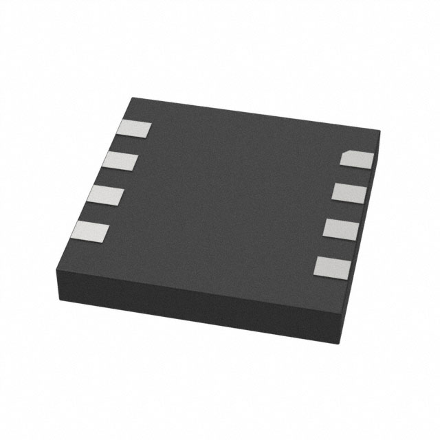
8-pin Grid-Array Quad Flat No-Lead (GQFN) package
■
Restriction of hazardous substances (RoHS) compliant
Cypress Semiconductor Corporation
Document Number: 002-18671 Rev. *L
•
The Excelon LP CY15X104QI is a low power, 4-Mbit nonvolatile
memory employing an advanced ferroelectric process. A ferroelectric random access memory or F-RAM is nonvolatile and
performs reads and writes similar to a RAM. It provides reliable
data retention for 151 years while eliminating the complexities,
overhead, and system-level reliability problems caused by serial
flash, EEPROM, and other nonvolatile memories.
Unlike serial flash and EEPROM, the CY15X104QI performs
write operations at bus speed. No write delays are incurred. Data
is written to the memory array immediately after each byte is
successfully transferred to the device. The next bus cycle can
commence without the need for data polling. In addition, the
product offers substantial write endurance compared to other
nonvolatile memories. The CY15X104QI is capable of
supporting 1015 read/write cycles, or 1000 million times more
write cycles than EEPROM.
These capabilities make the CY15X104QI ideal for nonvolatile
memory applications, requiring frequent or rapid writes.
Examples range from data collection, where the number of write
cycles may be critical, to demanding industrial controls where the
long write time of serial flash or EEPROM can cause data loss.
The CY15X104QI provides substantial benefits to users of serial
EEPROM or flash as a hardware drop-in replacement. The
CY15X104QI uses the high-speed SPI bus, which enhances the
high-speed write capability of F-RAM technology. The device
incorporates a read-only Device ID and Unique ID features,
which allow the host to determine the manufacturer, product
density, product revision, and unique ID for each part. The device
also provides a writable, 8-byte serial number registers, which
can be used to identify a specific board or a system.
For a complete list of related resources, click here.
198 Champion Court
•
San Jose, CA 95134-1709
•
408-943-2600
Revised July 15, 2019
�CY15B104QI
CY15V104QI
Logic Block Diagram
WP
256-Byte
Special Sector
F-RAM
CS
SCK
SI
Instruction Decoder
Control Logic
Write Protect
F-RAM Control
Data I/O Register
512K x 8
F-RAM Array
SO
Nonvolatile
Status Register
Device ID and Serial
Number Registers
Document Number: 002-18671 Rev. *L
Page 2 of 27
�CY15B104QI
CY15V104QI
Contents
Pinout ................................................................................ 4
Pin Definitions .................................................................. 4
Functional Overview ........................................................ 5
Memory Architecture ........................................................ 5
SPI Bus .............................................................................. 5
SPI Overview ............................................................... 5
Terms used in SPI Protocol ......................................... 5
SPI Modes ................................................................... 6
Power-Up to First Access ............................................ 6
Functional Description ..................................................... 7
Command Structure .................................................... 7
Maximum Ratings ........................................................... 17
Operating Range ............................................................. 17
DC Electrical Characteristics ........................................ 17
Data Retention and Endurance ..................................... 19
Capacitance .................................................................... 19
Thermal Resistance ........................................................ 19
Document Number: 002-18671 Rev. *L
AC Test Conditions ........................................................ 19
AC Switching Characteristics ....................................... 20
Power Cycle Timing ....................................................... 22
Ordering Information ...................................................... 23
Ordering Code Definitions ......................................... 23
Package Diagram ............................................................ 24
Acronyms ........................................................................ 25
Document Conventions ................................................. 25
Units of Measure ....................................................... 25
Document History Page ................................................. 26
Sales, Solutions, and Legal Information ...................... 30
Worldwide Sales and Design Support ....................... 30
Products .................................................................... 30
PSoC® Solutions ...................................................... 30
Cypress Developer Community ................................. 30
Technical Support ..................................................... 30
Page 3 of 27
�CY15B104QI
CY15V104QI
Pinout
Figure 1. 8-pin GQFN Pinout
CS
1
8
VDD
SO
2
7
DNU
WP
3
6
SCK
VSS
4
5
SI
TOP View
(Not to Scale)
Pin Definitions
Pin Name
I/O Type
Description
CS
Input
Chip Select. This active LOW input activates the device. When HIGH, the device enters low-power
standby mode, ignores other inputs, and the output is tristated. When LOW, the device internally
activates the SCK signal. A falling edge on CS must occur before every opcode.
SCK
Input
Serial Clock. All I/O activity is synchronized to the serial clock. Inputs are latched on the rising edge
and outputs occur on the falling edge of the serial clock. The clock frequency may be any value
between 0 and 20 MHz and may be interrupted at any time due to its synchronous behavior.
SI [1]
Input
Serial Input. All data is input to the device on this pin. The pin is sampled on the rising edge of SCK
and is ignored at other times. It should always be driven to a valid logic level to meet the power (IDD)
specifications.
SO [1]
Output
Serial Output. This is the data output pin. It is driven during a read and remains tristated at all other
times. Data transitions are driven on the falling edge of the serial clock SCK.
WP
Input
Write Protect. This Active LOW pin prevents write operation to the Status Register when WPEN bit
in the Status Register is set to ‘1’. This is critical because other write protection features are controlled
through the Status Register. A complete explanation of write protection is provided in Status Register
and Write Protection on page 9. This pin has an internal weak pull up resistor which keeps this pin
HIGH if left floating (not connected on the board). This pin can also be tied to VDD if not used.
DNU
Do Not Use
Do Not Use. Either leave this pin floating (not connected on the board) or tie to VDD.
VSS
Power supply Ground for the device. Must be connected to the ground of the system.
VDD
Power supply Power supply input to the device.
Note
1. SI may be connected to SO for a single pin data interface.
Document Number: 002-18671 Rev. *L
Page 4 of 27
�CY15B104QI
CY15V104QI
Functional Overview
The CY15X104QI is a serial F-RAM memory. The memory array
is logically organized as 524,288 × 8 bits and is accessed using
an industry-standard serial peripheral interface (SPI) bus. The
functional operation of the F-RAM is similar to serial flash and
serial EEPROMs. The major difference between the
CY15X104QI and a serial flash or EEPROM with the same
pinout is the F-RAM’s superior write performance, high
endurance, and low power consumption.
Memory Architecture
When accessing the CY15X104QI, the user addresses 512K
locations of eight data bits each. These eight data bits are shifted
in or out serially. The addresses are accessed using the SPI
protocol, which includes a chip select (to permit multiple devices
on the bus), an opcode, and a three-byte address. The upper
four bits of the address range are ‘don’t care’ values. The
complete address of 20 bits specifies each byte address
uniquely.
Most functions of the CY15X104QI are either controlled by the
SPI interface or handled by on-board circuitry. The access time
for the memory operation is essentially zero, beyond the time
needed for the serial protocol. That is, the memory is read or
written at the speed of the SPI bus. Unlike a serial flash or
EEPROM, it is not necessary to poll the device for a ready
condition because writes occur at bus speed. By the time a new
bus transaction can be shifted into the device, a write operation
is complete. This is explained in more detail in the interface
section.
SPI Bus
The CY15X104QI is an SPI slave device and operates at speeds
of up to 20 MHz. This high-speed serial bus provides high-performance serial communication to an SPI master. Many common
microcontrollers have hardware SPI ports allowing a direct
interface. It is simple to emulate the port using ordinary port pins
for microcontrollers that do not have this feature. The
CY15X104QI operates in SPI Modes 0 and 3.
SPI Overview
The SPI is a four-pin interface with Chip Select (CS), Serial Input
(SI), Serial Output (SO), and Serial Clock (SCK) pins.
The SPI is a synchronous serial interface, which uses clock and
data pins for memory access and supports multiple devices on
the data bus. A device on the SPI bus is activated using the CS
pin.
The relationship between chip select, clock, and data is dictated
by the SPI mode. This device supports SPI modes 0 and 3. In
both of these modes, data is clocked into the F-RAM on the rising
edge of SCK starting from the first rising edge after CS goes
active.
Document Number: 002-18671 Rev. *L
The SPI protocol is controlled by opcodes. These opcodes
specify the commands from the bus master to the slave device.
After CS is activated, the first byte transferred from the bus
master is the opcode. Following the opcode, any addresses and
data are then transferred. The CS must go inactive after an
operation is complete and before a new opcode can be issued.
Terms used in SPI Protocol
The commonly used terms in the SPI protocol are as follows.
SPI Master
The SPI master device controls the operations on the SPI bus.
An SPI bus may have only one master with one or more slave
devices. All the slaves share the same SPI bus lines and the
master may select any of the slave devices using the CS pin. All
of the operations must be initiated by the master activating a
slave device by pulling the CS pin of the slave LOW. The master
also generates the SCK and all the data transmission on SI and
SO lines are synchronized with this clock.
SPI Slave
The SPI slave device is activated by the master through the Chip
Select line. A slave device gets the SCK as an input from the SPI
master and all the communication is synchronized with this
clock. An SPI slave never initiates a communication on the SPI
bus and acts only on the instruction from the master.
The CY15X104QI operates as an SPI slave and may share the
SPI bus with other SPI slave devices.
Chip Select (CS)
To select any slave device, the master needs to pull down the
corresponding CS pin. Any instruction can be issued to a slave
device only while the CS pin is LOW. When the device is not
selected, data through the SI pin is ignored and the serial output
pin (SO) remains in a high-impedance state.
Note A new instruction must begin with the falling edge of CS.
Therefore, only one opcode can be issued for each active Chip
Select cycle.
Serial Clock (SCK)
The serial clock is generated by the SPI master and the
communication is synchronized with this clock after CS goes
LOW.
The CY15X104QI supports SPI modes 0 and 3 for data
communication. In both of these modes, the inputs are latched
by the slave device on the rising edge of SCK and outputs are
issued on the falling edge. Therefore, the first rising edge of SCK
signifies the arrival of the first Most Significant Bit (MSb) of an
SPI instruction on the SI pin. Further, all data inputs and outputs
are synchronized with SCK.
Page 5 of 27
�CY15B104QI
CY15V104QI
Data Transmission (SI/SO)
Serial Opcode
The SPI data bus consists of two lines, SI and SO, for serial data
communication. SI is also referred to as Master Out Slave In
(MOSI) and SO is referred to as Master In Slave Out (MISO). The
master issues instructions to the slave through the SI pin, while
the slave responds through the SO pin. Multiple slave devices
may share the SI and SO lines as described earlier.
After the slave device is selected with CS going LOW, the first
byte received is treated as the opcode for the intended operation.
CY15X104QI uses the standard opcodes for memory accesses.
The CY15X104QI has two separate pins for SI and SO, which
can be connected with the master as shown in Figure 2. For a
microcontroller that has no dedicated SPI bus, a
general-purpose port may be used. To reduce hardware
resources on the controller, it is possible to connect the two data
pins (SI, SO) together and tie off (HIGH) the WP pin. Figure 3
shows such a configuration, which uses only three pins.
Invalid Opcode
If an invalid opcode is received, the opcode is ignored and the
device ignores any additional serial data on the SI pin until the
next falling edge of CS, and the SO pin remains tristated.
Status Register
CY15X104QI has an 8-bit Status Register. The bits in the Status
Register are used to configure the device. These bits are
described in Table 3 on page 9.
SPI Modes
Figure 2. System Configuration with SPI Port
CY15X104QI may be driven by a microcontroller with its SPI
peripheral running in either of the following two modes:
SCK
MOSI
MISO
SCK
SPI Hostcontroller
or
SPI Master
SI
SO
SCK
CY15x104QI
CS
SI
SO
CY15x104QI
WP
CS
WP
CS1
WP1
CS2
WP2
Figure 3. System Configuration without SPI Port
P1.0
P1.1
SPI Hostcontroller
or
SPI Master
SCK
SI
SO
■
SPI Mode 0 (CPOL = 0, CPHA = 0)
■
SPI Mode 3 (CPOL = 1, CPHA = 1)
For both these modes, the input data is latched in on the rising
edge of SCK starting from the first rising edge after CS goes
active. If the clock starts from a HIGH state (in mode 3), the first
rising edge after the clock toggles is considered. The output data
is available on the falling edge of SCK. The two SPI modes are
shown in Figure 4 and Figure 5. The status of the clock when the
bus master is not transferring data is:
■
SCK remains at 0 for Mode 0
■
SCK remains at 1 for Mode 3
The device detects the SPI mode from the status of the SCK pin
when the device is selected by bringing the CS pin LOW. If the
SCK pin is LOW when the device is selected, SPI Mode 0 is
assumed and if the SCK pin is HIGH, it works in SPI Mode 3.
Figure 4. SPI Mode 0
CS
0
CY15x104QI
1
2
3
4
5
6
7
SCK
CS
WP
SI
7
6
5
4
3
2
1
0
P1.2
Figure 5. SPI Mode 3
Most Significant Bit (MSb)
The SPI protocol requires that the first bit to be transmitted is the
MSb. This is valid for both address and data transmission.
The 4-Mbit serial F-RAM requires a 3-byte address for any read
or write operation. Because the address is only 19 bits, the first
five bits, which are fed in are ignored by the device. Although
these four bits are ‘don’t care’, Cypress recommends that these
bits be set to 0s to enable seamless transition to higher memory
densities.
Document Number: 002-18671 Rev. *L
CS
0
1
2
3
4
5
6
7
SCK
SI
7
6
5
4
3
2
1
0
Power-Up to First Access
The CY15X104QI is not accessible for a tPU time after power-up.
Users must comply with the timing parameter, tPU, which is the
minimum time from VDD (min) to the first CS LOW. Refer to
Power Cycle Timing on page 22 for details.
Page 6 of 27
�CY15B104QI
CY15V104QI
Functional Description
Command Structure
There are 15 commands, called opcodes, that can be issued by the bus master to the CY15X104QI (see Table 1). These opcodes
control the functions performed by the memory.
Table 1. Opcode Commands
Name
Description
Opcode
Hex
Binary
Write Enable Control
WREN
Set write enable latch
06h
0000 0110b
WRDI
Reset write enable latch
04h
0000 0100b
RDSR
Read Status Register
05h
0000 0101b
WRSR
Write Status Register
01h
0000 0001b
Write memory data
02h
0000 0010b
READ
Read memory data
03h
0000 0011b
FSTRD
Fast read memory data
0Bh
0000 1011b
Register Access
Memory Write
WRITE
Memory Read
Special Sector Memory Access
SSWR
Special Sector Write
42h
0100 0010b
SSRD
Special Sector Read
4Bh
0100 1011b
Identification & Serial Number
RDID
Read device ID
9Fh
1001 1111b
RUID
Read Unique ID
4Ch
0100 1100b
WRSN
Write Serial Number
C2h
1100 0010b
RDSN
Read Serial Number
C3h
11000 011b
Low Power Modes
DPD
Enter Deep Power-Down
BAh
1011 1010b
HBN
Enter Hibernate Mode
B9h
1011 1001b
Reserved
Reserved
Document Number: 002-18671 Rev. *L
Unused opcodes are reserved for future use.
Page 7 of 27
�CY15B104QI
CY15V104QI
Write Enable Control Commands
Reset Write Enable Latch (WRDI, 04h)
Set Write Enable Latch (WREN, 06h)
The WRDI command disables all write activity by clearing the
Write Enable Latch. Verify that the writes are disabled by reading
the WEL bit in the Status Register and verify that WEL is equal
to ‘0’. Figure 7 illustrates the WRDI command bus configuration.
The CY15X104QI will power up with writes disabled. The WREN
command must be issued before any write operation. Sending
the WREN opcode allows the user to issue subsequent opcodes
for write operations. These include writing to the Status Register
(WRSR), the memory (WRITE), Special Sector (SSWR), and
Write Serial Number (WRSN).
Sending the WREN opcode causes the internal Write Enable
Latch to be set. A flag bit in the Status Register, called WEL,
indicates the state of the latch. WEL = ‘1’ indicates that writes are
permitted. Attempting to write the WEL bit in the Status Register
has no effect on the state of this bit - only the WREN opcode can
set this bit. The WEL bit will be automatically cleared on the rising
edge of CS following a WRDI, a WRSR, a WRITE, a SSWR, or
a WRSN operation. This prevents further writes to the Status
Register or the F-RAM array without another WREN command.
Figure 6 illustrates the WREN command bus configuration.
Figure 7. WRDI Bus Configuration
CS
0
1
2
3
4
5
6
7
SCK
SI
SI
0
0
0
0
0
1
0
0
Hi-Z
Opcode (04h)
Figure 6. WREN Bus Configuration
CS
0
Mode 3
1
2
3
4
5
6
7
SCK
Mode 0
SI
SI
0
0
0
0
0
1
1
0
Hi-Z
Opcode (06h)
Document Number: 002-18671 Rev. *L
Page 8 of 27
�CY15B104QI
CY15V104QI
Register Access Commands
Status Register and Write Protection
The write protection features of the CY15X104QI are multi-tiered and are enabled through the status register. The Status Register is
organized as follows. (The default value shipped from the factory for WEL, BP0, BP1, bits 4–5, and WPEN is ‘0’, and for bit 6 is ‘1’.)
Table 2. Status Register
Bit 7
Bit 6
Bit 5
Bit 4
Bit 3
Bit 2
Bit 1
Bit 0
WPEN (0)
X (1)
X (0)
X (0)
BP1 (0)
BP0 (0)
WEL (0)
X (0)
Table 3. Status Register Bit Definition
Bit
Definition
Description
Bit 0
Don’t care
Bit 1 (WEL)
Write Enable
This bit is non-writable and always returns ‘0’ upon read.
Bit 2 (BP0)
Block Protect bit ‘0’
Used for block protection. For details, see Table 4.
Bit 3 (BP1)
Block Protect bit ‘1’
Used for block protection. For details, see Table 4.
WEL indicates if the device is write enabled. This bit defaults to ‘0’ (disabled) on power-up.
WEL = ‘1’ --> Write enabled
WEL = ‘0’ --> Write disabled
Bit 4–5
Don’t care
These bits are non-writable and always return ‘0’ upon read.
Bit 6
Don’t care
This bit is non-writable and always returns ‘1’ upon read.
Bit 7 (WPEN)
Write Protect Enable bit Used to enable the function of Write Protect Pin (WP). For details, see Table 5.
Bits 0 and 4–5 are fixed at ‘0’ and bit 6 is fixed at ‘1’; none of these
bits can be modified. Note that bit 0 (“Ready or Write in progress”
bit in serial flash and EEPROM) is unnecessary, as the F-RAM
writes in real-time and is never busy, so it reads out as a ‘0’. An
exception to this is when the device is waking up either from
Deep Power-Down Mode (DPD, BAh) or Hibernate Mode (HBN,
B9h). The BP1 and BP0 control the software write-protection
features and are nonvolatile bits. The WEL flag indicates the
state of the Write Enable Latch. Attempting to directly write the
WEL bit in the Status Register has no effect on its state. This bit
is internally set and cleared via the WREN and WRDI
commands, respectively.
BP1 and BP0 are memory block write protection bits. They
specify portions of memory that are write-protected as shown in
Table 4.
Table 4. Block Memory Write Protection
BP1
BP0
0
0
0
1
The BP1 and BP0 bits and the Write Enable Latch are the only
mechanisms that protect the memory from writes. The remaining
write protection features protect inadvertent changes to the block
protect bits.
The write protect enable bit (WPEN) in the Status Register
controls the effect of the hardware write protect (WP) pin. Refer to
Figure 23 on page 21 for the WP pin timing diagram. When the
WPEN bit is set to ‘0’, the status of the WP pin is ignored. When
the WPEN bit is set to ‘1’, a LOW on the WP pin inhibits a write to
the Status Register. Thus the Status Register is write-protected
only when WPEN = ‘1’ and WP = ‘0’. Table 5 summarizes the
write protection conditions.
Table 5. Write Protection
WEL WPEN WP
Protected Unprotected
Blocks
Blocks
Status
Register
Protected
0
X
X
Protected
None
1
0
X
Protected
Unprotected Unprotected
60000h to 7FFFFh (upper 1/4)
1
1
0
Protected
Unprotected
1
1
1
Protected
Unprotected Unprotected
Protected Address Range
1
0
40000h to 7FFFFh (upper 1/2)
1
1
00000h to 7FFFFh (all)
Document Number: 002-18671 Rev. *L
Protected
Protected
Page 9 of 27
�CY15B104QI
CY15V104QI
Read Status Register (RDSR, 05h)
The RDSR command allows the bus master to verify the contents of the Status Register. Reading the status register provides
information about the current state of the write-protection features. Following the RDSR opcode, the CY15X104QI will return one byte
with the contents of the Status Register.
Figure 8. RDSR Bus Configuration
CS
0
1
2
3
4
5
6
7
0
1
2
3
4
5
6
D3
D2
D1
7
SCK
SI
0
0
0
0
0
1
0
Hi-Z
SO
Hi-Z
1
D7 D6
D5
D4
MSb
D0
LSb
Opcode (05h)
Read Data
Write Status Register (WRSR, 01h)
that on the CY15X104QI, WP only prevents writing to the Status
Register, not the memory array. Before sending the WRSR
command, the user must send a WREN command to enable
writes. Executing a WRSR command is a write operation and
therefore, clears the Write Enable Latch.
The WRSR command allows the SPI bus master to write into the
Status Register and change the write protect configuration by
setting the WPEN, BP0, and BP1 bits as required. Before issuing
a WRSR command, the WP pin must be HIGH or inactive. Note
Figure 9. WRSR Bus Configuration (WREN not shown)
CS
0
1
2
3
4
5
6
7
0
1
2
3
4
5
6
7
D7 D6
D5
D4
D3
D2
D1
D0
SCK
SI
0
0
0
0
0
0
0
1
MSb
LSb
Hi-Z
SO
Opcode (01h)
Write Data
the last address of 7FFFFh is reached, the internal address
counter will roll over to 00000h. Every data byte to be written is
transmitted on SI in 8-clock cycles with MSb first and the LSb
last. The rising edge of CS terminates a write operation. The
CY15X104QI write operation is shown in Figure 10.
Memory Operation
The SPI interface, which is capable of a high clock frequency,
highlights the fast write capability of the F-RAM technology.
Unlike serial flash and EEPROMs, the CY15X104QI can perform
sequential writes at bus speed. No page register is needed and
any number of sequential writes may be performed.
Notes
Memory Write Operation Commands
Write Operation (WRITE, 02h)
All writes to the memory begin with a WREN opcode with CS
being asserted and deasserted. The next opcode is WRITE. The
WRITE opcode is followed by a three-byte address containing
the 19-bit address (A18–A0) of the first data byte to be written
into the memory. The upper five bits of the three-byte address
are ignored. Subsequent bytes are data bytes, which are written
sequentially. Addresses are incremented internally as long as
the bus master continues to issue clocks and keeps CS LOW. If
■
When a burst write reaches a protected block address, the
automatic address increment stops and all the subsequent data
bytes received for write will be ignored by the device.
EEPROMs use page buffers to increase their write throughput.
This compensates for the technology’s inherently slow write
operations. F-RAM memories do not have page buffers
because each byte is written to the F-RAM array immediately
after it is clocked in (after the eighth clock). This allows any
number of bytes to be written without page buffer delays.
■
If power is lost in the middle of the write operation, only the last
completed byte will be written.
Figure 10. Memory Write (WREN not shown) Operation
CS
0
1
2
3
4
5
6
7
0
1
2
3
A22
A21
A20
4
20
21
22
23
0
1
2
3
4
5
6
D7 D6
MSb
D5
D4
D3
D2
D1
7
SCK
SI
0
0
SO
0
0
0
0
Opcode (02h)
Document Number: 002-18671 Rev. *L
1
0
A23
A3
Hi-Z
A2
A1
A0
D0
LSb
Hi-Z
Address
Write Data
Page 10 of 27
�CY15B104QI
CY15V104QI
during read data bytes. Subsequent bytes are data bytes, which
are read out sequentially. Addresses are incremented internally
as long as the bus master continues to issue clocks and CS is
LOW. If the last address of 7FFFFh is reached, the internal
address counter will roll over to 00000h. Every data byte to be
written is transmitted on SI in 8-clock cycles with MSb first and
the LSb last. The rising edge of CS terminates a read operation
and tristates the SO pin. The CY15X104QI read operation is
shown in Figure 11.
Memory Read Commands
Read Operation (READ, 03h)
After the falling edge of CS, the bus master can issue a READ
opcode. Following the READ command is a three-byte address
containing the 19-bit address (A18–A0) of the first byte of the
read operation. The upper five bits of the address are ignored.
After the opcode and address are issued, the device drives out
the read data on the next eight clocks. The SI input is ignored
Figure 11. Memory Read Operation
CS
0
1
2
3
4
5
6
7
0
1
2
3
A22
A21
A20
4
20
21
22
23
0
1
2
3
4
5
6
D3
D2
D1
7
SCK
0
SI
0
0
0
0
0
1
1
A23
A3
A2
A1
Hi-Z
SO
Hi-Z
A0
D7 D6
D5
D4
MSb
Opcode (03h)
D0
LSb
Address
Read Data
available. In case of bulk read, the internal address counter is
incremented automatically, and after the last address 7FFFFh is
reached, the internal address counter rolls over to 00000h. When
the device is driving data on its SO line, any transition on its SI
line is ignored. The rising edge of CS terminates a fast read
operation and tristates the SO pin. The CY15X104QI Fast Read
operation is shown in Figure 12.
Fast Read Operation (FAST_READ, 0Bh)
The CY15X104QI supports a FAST READ opcode (0Bh) that is
provided for opcode compatibility with serial flash devices. The
FAST READ opcode is followed by a three-byte address
containing the 19-bit address (A18–A0) of the first byte of the
read operation and then a dummy byte. The dummy byte inserts
a read latency of 8-clock cycle. The fast read operation is
otherwise the same as an ordinary read operation except that it
requires an additional dummy byte. After receiving the opcode,
address, and a dummy byte, the CY15X104QI starts driving its
SO line with data bytes, with MSb first, and continues
transmitting as long as the device is selected and the clock is
Note The dummy byte can be any 8-bit value but Axh
(8’b1010xxxx). The lower 4 bits of Axh are don’t care bits. Hence,
Axh essentially represents 16 different 8-bit values which
shouldn’t be transmitted as the dummy byte. 00h is typically used
as the dummy byte in most use cases.
Figure 12. Fast Read Operation
CS
0
1
2
3
4
5
6
7
0
1
2
3
A22
A21
A20
4
20
21
22
23
0
1
2
3
4
5
6
7
0
1
2
3
4
5
6
D3
D2
D1
7
SCK
SI
SO
0
0
0
0
1
0
1
1
Hi-Z
A23
A3
MSb
A2
A1
A0
x
x
x
x
x
x
x
Hi-Z
x
LSb
D7 D6
D5
D4
MSb
Opcode (0Bh)
Document Number: 002-18671 Rev. *L
Address
Dummy Byte
D0
LSb
Read Data
Page 11 of 27
�CY15B104QI
CY15V104QI
the ongoing SSWR operation. Every data byte to be written is
transmitted on SI in 8-clock cycles with MSb first and the LSb
last. The rising edge of CS terminates a write operation. The
CY15X104QI special sector write operation is shown in
Figure 13.
Special Sector Memory Access Commands
Special Sector Write (SSWR, 42h)
All writes to the 256-byte special begin with a WREN opcode with
CS being asserted and deasserted. The next opcode is SSWR.
The SSWR opcode is followed by a three-byte address
containing the 8-bit sector address (A7–A0) of the first data byte
to be written into the special sector memory. The upper 16 bits
of the three-byte address are ignored. Subsequent bytes are
data bytes, which are written sequentially. Addresses are incremented internally as long as the bus master continues to issue
clocks and keeps CS LOW. Once the internal address counter
auto increments to XXXFFh, CS should toggle HIGH to terminate
Notes
■
If power is lost in the middle of the write operation, only the last
completed byte will be written.
■
The special sector F-RAM memory guarantees to retain data
integrity up to three cycles of standard reflow soldering.
Figure 13. Special Sector Write (WREN not shown) Operation
CS
0
1
2
3
4
5
6
7
0
1
2
3
A22
A21
A20
4
20
21
22
23
0
1
2
3
4
5
6
D6
D5
D4
D3
D2
D1
7
SCK
SI
0
1
0
0
0
0
1
A23
0
A3
A2
A1
A0
D7
D0
MSb
LSb
Hi-Z
SO
Hi-Z
Opcode (42h)
Address
Write Data
issue clocks and CS is LOW. Once the internal address counter
auto increments to XXXFFh, CS should toggle HIGH to terminate
the ongoing SSRD operation. Every read data byte on SO is
driven in 8-clock cycles with MSb first and the LSb last. The rising
edge of CS terminates a special sector read operation and
tristates the SO pin. The CY15X104QI special sector read
operation is shown in Figure 14.
Special Sector Read (SSRD, 4Bh)
After the falling edge of CS, the bus master can issue an SSRD
opcode. Following the SSRD command is a three-byte address
containing the 8-bit address (A7–A0) of the first byte of the
special sector read operation. The upper 16 bits of the address
are ignored. After the opcode and address are issued, the device
drives out the read data on the next eight clocks. The SI input is
ignored during read data bytes. Subsequent bytes are data
bytes, which are read out sequentially. Addresses are
incremented internally as long as the bus master continues to
Note The special sector F-RAM memory guarantees to retain
data integrity up to three cycles of standard reflow soldering.
Figure 14. Special Sector Read Operation
CS
0
1
2
3
4
5
6
7
0
1
2
3
A22
A21
A20
4
20
21
22
23
0
1
2
3
4
5
6
D3
D2
D1
7
SCK
SI
SO
0
1
0
0
1
0
1
1
A23
A3
Hi-Z
A2
A1
Hi-Z
A0
D7 D6
D5
D4
MSb
Opcode (4Bh)
Document Number: 002-18671 Rev. *L
Address
D0
LSb
Read Data
Page 12 of 27
�CY15B104QI
CY15V104QI
the continuation code 7Fh followed by the single byte C2h. There
are two bytes of product ID, which includes a family code, a
density code, a sub code, and the product revision code. Table 6
shows 9-Byte Device ID field description. Refer to Ordering
Information on page 23 for 9-Byte device ID of an individual part.
The CY15X104QI read device ID operation is shown in
Figure 15.
Identification and Serial Number Commands
Read Device ID (RDID, 9Fh)
The CY15X104QI device can be interrogated for its
manufacturer, product identification, and die revision. The RDID
opcode 9Fh allows the user to read the 9-byte manufacturer ID
and product ID, both of which are read-only bytes. The
JEDEC-assigned manufacturer ID places the Cypress
(Ramtron) identifier in bank 7; therefore, there are six bytes of
Note The least significant data byte (Byte 0) shifts out first and
the most significant data byte (Byte 8) shifts out last.
Table 6. 9-Byte Device ID
Device ID Field Description
Manufacturer ID
[71:16]
Family
[15:13]
Density
[12:9]
Inrush
[8]
Sub Type
[7:5]
Revision
[4:3]
Voltage
[2]
Frequency
[1:0]
56-bit
3-bit
4-bit
1-bit
3-bit
2-bit
1-bit
2-bit
Figure 15. Read Device ID
CS
0
1
2
3
4
5
6
7
0
1
2
3
4
60
61
62
63
64
65
66
67
68
69
70
71
SCK
SI
1
0
0
1
1
1
1
MSb
Hi-Z
SO
Hi-Z
1
D7
LSb
D6
D5
D4
D3
D2
D1
D0
D7
D6
D5
D4
D3
D2
Byte 0
D1
D0
Byte 8
Opcode (9Fh)
9-Byte Device ID
Read Unique ID (RUID, 4Ch)
Notes
The CY15X102QN device can be interrogated for unique ID
which is a factory programmed, 64-bit number unique to each
device. The RUID opcode, 4Ch allows to read the 8-byte, read
only unique ID. The CY15X102QN read unique ID operation is
shown in Figure 16.
■
The least significant data byte (Byte 0) shifts out first and the
most significant data byte (Byte 7) shifts out last.
■
The unique ID registers are guaranteed to retain data integrity
of up to three cycles of the standard reflow soldering.
Figure 16. Read Unique ID
CS
0
1
2
3
4
5
6
7
0
1
2
3
4
52
53
54
55
56
57
58
59
60
61
62
63
SCK
SI
SO
0
1
0
0
1
1
Hi-Z
0
Hi-Z
0
MSb
D7
LSb
D6
D5
D4
D3
D2
D1
D0
D7
D6
Byte 0
Opcode (4Ch)
Document Number: 002-18671 Rev. *L
D5
D4
D3
D2
D1
D0
Byte 7
8-Byte Unique ID
Page 13 of 27
�CY15B104QI
CY15V104QI
Write Serial Number (WRSN, C2h)
8 bytes of serial number. After the last byte of the serial number
is shifted in, CS must be driven high to complete the WRSN
operation. The CY15X104QI write serial number operation is
shown in Figure 17.
The serial number is an 8-byte one-time programmable memory
space provided to the user to uniquely identify a PC board or a
system. A serial number typically consists of a two-byte
Customer ID, followed by five bytes of a unique serial number
and one byte of CRC check. However, the end application can
define its own format for the 8-byte serial number. All writes to
the Serial Number Register begin with a WREN opcode with CS
being asserted and deasserted. The next opcode is WRSN. The
WRSN instruction can be used in burst mode to write all the
Note The CRC checksum is not calculated by the device. The
system firmware must calculate the CRC checksum on the
7-byte content and append the checksum to the 7-byte
user-defined serial number before programming the 8-byte serial
number into the serial number register. The factory default value
for the 8-byte Serial Number is ‘0000000000000000h’.
Table 7. 8-Byte Serial Number
16-bit Customer Identifier
SN[63:56]
40-bit Unique Number
SN[55:48]
SN[47:40]
SN[39:32]
SN[31:24]
8-bit CRC
SN[23:16]
SN[15:8]
SN[7:0]
Figure 17. Write Serial Number (WREN not shown) Operation
CS
0
1
2
3
4
5
6
7
0
1
2
D6
D5
3
4
52
53
54
55
56
57
58
59
60
61
62
63
SCK
SI
1
1
0
0
0
0
1
0
D7
D4
D3
D2
D1
D0
D7 D6
D5
D4
D3
D2
D1
D0
LSb
MSb
Hi-Z
SO
Hi-Z
Opcode (C2h)
Write 8-Byte Serial Number
Read Serial Number (RDSN, C3h)
loops back to the first (MSb) byte of the serial number. An RDSN
instruction can be issued by shifting the opcode for RDSN after
CS goes LOW. The CY15X104QI read serial number operation
is shown in Figure 18.
The CY15X104QI device incorporates an 8-byte serial space
provided to the user to uniquely identify the device. The serial
number is read using the RDSN instruction. A serial number read
may be performed in burst mode to read all the eight bytes at
once. After the last byte of the serial number is read, the device
Note The least significant data byte (Byte 0) shifts out first and
the most significant data byte (Byte 7) shifts out last.
Figure 18. Read Serial Number Operation
CS
0
1
2
3
4
5
6
7
0
1
2
3
4
52
53
54
55
56
57
58
59
60
61
62
63
SCK
SI
SO
1
1
0
0
0
0
Hi-Z
1
Hi-Z
1
MSb
D7
LSb
D6
D5
D4
D3
D2
D1
D0
D7
D6
Byte 0
Opcode (C3h)
Document Number: 002-18671 Rev. *L
D5
D4
D3
D2
D1
D0
Byte 7
8-Byte Serial Number
Page 14 of 27
�CY15B104QI
CY15V104QI
A CS pulse-width of tCSDPD exits the DPD mode after tEXTDPD
time. The CS pulse-width can be generated either by sending a
dummy command cycle or toggling CS alone while SCK and I/Os
are don’t care. The I/Os remain in hi-Z state during the wakeup
from deep power-down. Refer to Figure 19 for DPD entry and
Figure 20 for DPD exit timing.
Low Power Mode Commands
Deep Power-Down Mode (DPD, BAh)
A power-saving Deep Power-Down mode is implemented on the
CY15X104QI device. The device enters the Deep Power-Down
mode after tENTDPD time after the DPD opcode BAh is clocked in
and a rising edge of CS is applied. When in Deep Power-Down
mode, the SCK and SI pins are ignored and SO will be Hi-Z, but
the device continues to monitor the CS pin.
Figure 19. DPD Entry Timing
Enters DPD
tENTDPD
CS
0
1
2
3
4
5
6
7
SCK
SI
1
0
1
1
1
0
1
0
hi-Z
SO
Opcode (BAh)
Figure 20. DPD Exit Timing
tEXTDPD
tCSDPD
CS
0
1
2
SCK
tSU
I/Os
Document Number: 002-18671 Rev. *L
X
Page 15 of 27
�CY15B104QI
CY15V104QI
will return to normal operation within tEXTHIB time. The SO pin
remains in a Hi-Z state during the wakeup from hibernate period.
The device does not necessarily respond to an opcode within the
wakeup period. To exit the Hibernate mode, the controller may
send a “dummy” read, for example, and wait for the remaining
tEXTHIB time.
Hibernate Mode (HBN, B9h)
A lowest power Hibernate mode is implemented on the
CY15X104QI device. The device enters Hibernate mode after
tENTHIB time after the HBN opcode B9h is clocked in and a rising
edge of CS is applied. When in Hibernate mode, the SCK and SI
pins are ignored and SO will be Hi-Z, but the device continues to
monitor the CS pin. On the next falling edge of CS, the device
Figure 21. Hibernate Mode Operation
Enters
Hibernate Mode
tENTHIB
Recovers from
Hibernate Mode
tEXTHIB
CS
0
1
2
3
4
5
6
0
7
1
2
SCK
tSU
SI
SO
1
0
1
1
1
0
0
1
hi-Z
Opcode (B9h)
Endurance
The CY15X104QI devices are capable of being accessed at
least 1015 times, reads or writes.
An F-RAM memory operates with a read and restore
mechanism. Therefore, an endurance cycle is applied on a row
basis for each access (read or write) to the memory array. The
F-RAM architecture is based on an array of rows and columns of
32K rows of 64-bit each. The entire row is internally accessed
once, whether a single byte or all eight bytes are read or written.
Each byte in the row is counted only once in an endurance calculation. Table 8 shows endurance calculations for a 64-byte
repeating loop, which includes an opcode, a starting address,
and a sequential 64-byte data stream. This causes each byte to
experience one endurance cycle through the loop.
F-RAM read and write endurance is virtually unlimited at a
20-MHz clock rate.
Table 8. Time to Reach Endurance Limit for Repeating 64-byte Loop
Years to Reach 1015 Limit
SCK Freq (MHz)
Endurance Cycles/sec
Endurance Cycles/year
20
36,520
1.16 × 10¹²
864
10
18,380
5.79 × 10¹¹
1727
5
9,190
2.90 × 10¹¹
3454
Document Number: 002-18671 Rev. *L
Page 16 of 27
�CY15B104QI
CY15V104QI
Maximum Ratings
Surface mount lead soldering temperature
(3 seconds) .............................................................. +260 °C
Exceeding the maximum ratings may impair the useful life of the
device. User guidelines are not tested.
DC output current
(1 output at a time, 1s duration) .................................. 15 mA
Storage temperature ................................ –65 °C to +125 °C
Maximum accumulated storage time
At 125 °C ambient temperature ................................. 1000 h
At 85 °C ambient temperature ............................... 10 Years
Electrostatic discharge voltage
Human Body Model (JEDEC Std JESD22-A114-B) ...... 2 kV
Charged Device Model
(JEDEC Std JESD22-C101-A) .................................... 500 V
Maximum junction temperature ................................ 125 °C
Latch-up current ..................................................... >140 mA
Supply voltage on VDD relative to VSS:
CY15V104QI: ..............................................–0.5 V to +2.4 V
CY15B104QI: ..............................................–0.5 V to +4.1 V
Operating Range
Device
Input voltage ............................................ VIN VDD + 0.5 V
Ambient
Temperature
Range
VDD
DC voltage applied to outputs
in High-Z state ................................... –0.5 V to VDD + 0.5 V
CY15V104QI Commercial 0 °C to +70 °C 1.71 V to 1.89 V
Transient voltage (< 20 ns)
on any pin to ground potential ........... –2.0 V to VDD + 2.0 V
CY15V104QI
CY15B104QI
1.8 V to 3.6 V
Industrial
–40 °C to +85 °C 1.71 V to 1.89 V
CY15B104QI
Package power dissipation capability
(TA = 25 °C) ................................................................. 1.0 W
1.8 V to 3.6 V
DC Electrical Characteristics
Over the Operating Range
Parameter
VDD
IDD
ISB
Typ [2, 3]
Max
1.71
1.8
1.89
1.8
3.3
3.6
–
0.2
0.35
–
1.2
1.4
–
0.2
0.4
–
1.2
1.5
–
0.3
0.45
–
1.3
1.5
–
0.3
0.6
–
1.3
1.6
VDD = 1.71 V to 1.89 V; TA = 25 °C
–
2.30
–
TA = 60 °C
–
–
20[3]
TA = 70 °C
–
–
30
TA = 85 °C
–
–
65
–
2.60
–
TA = 60 °C
–
–
20[3]
TA = 70 °C
–
–
31
TA = 85 °C
–
–
70
Description
Power supply
VDD supply current
VDD standby current
Test Conditions
CY15V104QI
–
CY15B104QI
VDD = 1.71 V to 1.89 V;
SCK toggling between
VDD – 0.2 V and VSS,
other inputs VSS or
VDD – 0.2 V.
SO = Open
VDD = 1.8 V to 3.6 V;
SCK toggling between
VDD – 0.2 V and VSS,
other inputs VSS or
VDD – 0.2 V.
SO = Open
CS = VDD.
All other inputs
VSS or VDD.
VDD = 1.8 V to 3.6 V;
CS = VDD.
All other inputs
VSS or VDD.
Temperature
fSCK = 1 MHz
fSCK = 20 MHz
Commercial
fSCK = 1 MHz
fSCK = 20 MHz
fSCK = 1 MHz
fSCK = 20 MHz
Industrial
Commercial
fSCK = 1 MHz
fSCK = 20 MHz
TA = 25 °C
Industrial
–
Min
Unit
V
mA
µA
Notes
2. Typical values are at 25 °C, VDD = VDD (typ).
3. This parameter is guaranteed by characterization; not tested in production.
Document Number: 002-18671 Rev. *L
Page 17 of 27
�CY15B104QI
CY15V104QI
DC Electrical Characteristics (continued)
Over the Operating Range
Parameter
IDPD
IHBN
IPEAK
Min
Typ [2, 3]
Max
–
0.70
–
–
–
5.0[4]
–
–
7.0
–
–
15
–
0.80
–
TA = 60 °C
–
–
5.50[4]
TA = 70 °C
–
–
8.0
TA = 85 °C
–
–
16
T = 25 °C
VDD = 1.71 V to 1.89 V; A
TA = 60 °C
CS = VDD.
All other inputs
TA = 70 °C
VSS or VDD.
TA = 85 °C
–
0.10
–
–
–
0.25[4]
–
–
0.40
–
–
0.90
–
0.10
–
TA = 60 °C
–
–
0.45[4]
TA = 70 °C
–
–
0.75
TA = 85 °C
–
–
1.6
–
1.50
1.65[4]
Description
Deep power-down
current
Hibernate mode
current
Peak current drawn
from VDD during
power-up, wake up
from Hibernate, wake
up from
Deep-power-Down,
or Standby mode.
Test Conditions
T = 25 °C
VDD = 1.71 V to 1.89 V; A
TA = 60 °C
CS = VDD.
All other inputs
TA = 70 °C
VSS or VDD.
TA = 85 °C
VDD = 1.8 V to 3.6 V;
CS = VDD.
All other inputs
VSS or VDD.
VDD = 1.8 V to 3.6 V;
CS = VDD.
All other inputs
VSS or VDD.
TA = 25 °C
TA = 25 °C
Temperature
–
–
VDD = 1.71 V to 1.89 V;
CS = VDD.
All other inputs VSS or VDD.
Averaged over 10 μs.
–
VDD = 1.8 V to 3.60 V;
CS = VDD.
All other inputs VSS or VDD.
Averaged over 10 μs.
–
–
1.60
1.80[4]
–1
–
1
–100
–
1
–
ILO
Output leakage
current
–
–1
–
1
VIH
Input HIGH voltage
–
0.7 × VDD
–
VDD + 0.3
VIL
Input LOW voltage
–
–0.3
–
0.3 × VDD
VOH1
Output HIGH voltage IOH = –1 mA, VDD = 2.7 V.
–
2.4
–
–
VOH2
Output HIGH voltage IOH = –100 A
–
VDD – 0.2
–
–
VOL1
Output LOW voltage IOL = 2 mA, VDD = 2.7 V
Output LOW voltage IOL = 150 µA
–
–
–
0.4
–
–
–
0.2
VOL2
VSS < VOUT < VDD
µA
µA
mA
Input leakage current
on I/O pins except WP
pin
VSS < VIN < VDD
Input leakage current
on WP pin
ILI
Unit
µA
V
Note
4. This parameter is guaranteed by characterization; not tested in production.
Document Number: 002-18671 Rev. *L
Page 18 of 27
�CY15B104QI
CY15V104QI
Data Retention and Endurance
Parameter
TDR
NVC
Description
Data retention
Endurance
Test condition
Min
Max
Unit
TA = 85 C
10
–
TA = 70 C
141
–
TA = 60 C
151
–
TA = 50 C
160
–
Over operating temperature
1015
–
Cycles
Max
Unit
Years
Capacitance
For all packages.
Parameter [5]
Description
CO
Output pin capacitance (SO)
CI
Input pin capacitance
Test Conditions
TA = 25 °C, f = 1 MHz, VDD = VDD (typ)
8
pF
6
Thermal Resistance
Parameter [5]
Test Conditions
8-pin GQFN
Package
Test conditions follow standard test methods and
procedures for measuring thermal impedance, per
EIA/JESD51.
118
Description
JA
Thermal resistance
(junction to ambient)
JC
Thermal resistance
(junction to case)
Unit
C/W
60
AC Test Conditions
Input pulse levels ................................ 10% and 90% of VDD
Input rise and fall times .................................................. 3 ns
Input and output timing reference levels ............... 0.5 × VDD
Output load capacitance ............................................. 30 pF
Note
5. This parameter is guaranteed by characterization; not tested in production.
Document Number: 002-18671 Rev. *L
Page 19 of 27
�CY15B104QI
CY15V104QI
AC Switching Characteristics
Over the Operating Range
Parameters [6]
Cypress
Parameter
Description
Alt.
Parameter
Min
Max
Unit
MHz
fSCK
–
SCK clock frequency
0
20
tCH
–
Clock HIGH time
22
–
–
Clock LOW time
22
–
–
Clock LOW to Output low-Z
0
–
tCSS
tCSU
Chip select setup
10
–
tCSH
tCSH
Chip select hold - SPI mode 0
10
–
tCSH1
–
Chip select hold - SPI mode 3
10
–
tHZCS[8, 9]
tOD
Output disable time
–
20
tCO
tODV
Output data valid time
–
20
tOH
–
Output hold time
1
–
tCS
tD
Deselect time
60
–
tSD
tSU
Data setup time
5
–
tHD
tH
Data hold time
5
–
tWPS
tWHSL
WP setup time (w.r.t CS)
20
–
tWPH
tSHWL
WP hold time (w.r.t CS)
20
–
tCL
tCLZ
[7]
ns
Notes
6. Test conditions assume a signal transition time of 3 ns or less, timing reference levels of 0.5 × VDD, input pulse levels of 10% to 90% of VDD, and output loading of
the specified IOL/IOH and 30-pF load capacitance shown in AC Test Conditions on page 19.
7. Guaranteed by design.
8. tHZCS is specified with a load capacitance of 5 pF. Transition is measured when the output enters a high-impedance state.
9. This parameter is guaranteed by characterization; not tested in production.
Document Number: 002-18671 Rev. *L
Page 20 of 27
�CY15B104QI
CY15V104QI
Figure 22. Synchronous Data Timing (Mode 0 and Mode 3)
tCS
CS
tCSS
tCH
tCL
tCSH1
tCSH
Mode 3
SCK Mode 0
tSD
SI
SO
X
tHD
X
VALID DATA IN
tCO
tCLZ
Hi-Z
tOH
X
tHZCS
X
DATA OUT
Hi-Z
Figure 23. Write Protect Timing During Write Status Register (WRSR) Operation
tWPS
tWPH
CS
0
1
2
3
4
5
6
7
0
1
2
3
4
5
6
7
D7 D6
D5
D4
D3
D2
D1
D0
SCK
SI
0
0
0
0
0
0
0
1
MSb
SO
Hi-Z
Opcode (01h)
Document Number: 002-18671 Rev. *L
LSb
Write Data
Page 21 of 27
�CY15B104QI
CY15V104QI
Power Cycle Timing
Over the Operating Range
Parameters[10]
Cypress
Parameter
tPU
tVR
[11]
tVF[11, 12]
tENTDPD[13]
Description
Min
Max
Unit
Power-up VDD(min) to first access (CS LOW)
5
–
ms
VDD power-up ramp rate
30
–
VDD power-down ramp rate
20
–
CS high to enter deep power-down (CS high to hibernate mode current)
–
3
0.015
4 1/fSCK
Recovery time from deep power down mode (CS low to ready for access)
–
150
Time to enter hibernate (CS high to hibernate mode current)
–
3
Alt.
Parameter
tDP
tCSDPD
CS pulse width to wake up from deep power-down mode
tEXTDPD
tRDP
tENTHIB[14]
tEXTHIB
Recovery time from hibernate mode (CS low to ready for access)
tREC
VDD(low)[12]
tPD[12]
µs/V
µs
–
5
ms
Low VDD where initialization must occur
0.6
–
V
VDD(low) time when VDD(low) at 0.6 V
130
–
VDD(low) time when VDD(low) at VSS
70
–
µs
Figure 24. Power Cycle Timing
VDD
VDD
VDD (max)
No Device Access
Allowed
VDD (max)
VDD (min)
VDD (min)
tVR
tPU
Device Access
Allowed
tVF tVR
tPU
Device Access
Allowed
VDD (low)
tPD
Time
Time
Notes
10. Test conditions assume a signal transition time of 3 ns or less, timing reference levels of 0.5 × VDD, input pulse levels of 10% to 90% of VDD, and output loading of
the specified IOL/IOH and 30-pF load capacitance shown in AC Test Conditions on page 19.
11. Slope measured at any point on the VDD waveform.
12. This parameter is guaranteed by characterization; not tested in production.
13. Guaranteed by design. Refer to Figure 19 on page 15 for Deep Power Down mode timing.
14. Guaranteed by design. Refer to Figure 21 on page 16 for Hibernate mode timing.
Document Number: 002-18671 Rev. *L
Page 22 of 27
�CY15B104QI
CY15V104QI
Ordering Information
Ordering Code
Package
Diagram
Device ID
CY15B104QI-20LPXC
CY15B104QI-20LPXCT
CY15B104QI-20LPXI
CY15B104QI-20LPXIT
Package Type
Operating
Range
7F7F7F7F7F7FC22DA1
Commercial
7F7F7F7F7F7FC22D01
Industrial
002-18131 8-pin GQFN
CY15V104QI-20LPXC
CY15V104QI-20LPXCT
CY15V104QI-20LPXI
CY15V104QI-20LPXIT
7F7F7F7F7F7FC22DA5
Commercial
7F7F7F7F7F7FC22D05
Industrial
All these parts are Pb-free. Contact your local Cypress sales representative for availability of these parts.
Ordering Code Definitions
CY
15
B
104
Q
I
- 20
LP
X
C
T
Options:
Blank = Standard; T = Tape and Reel
Temperature Range:
C = Commercial (0 °C to +70 °C)
I = Industrial (-40 °C to +85 °C)
X = Pb-free
Package Type:
LP = 8-pin GQFN
Frequency:
20 = 20 MHz
I = Inrush Current Control
Interface: Q = SPI F-RAM
Density: 104 = 4-Mbit
Voltage:
B = 1.8 V to 3.6 V
V = 1.71 V to 1.89 V
15 = F-RAM
CY = Cypress
Document Number: 002-18671 Rev. *L
Page 23 of 27
�CY15B104QI
CY15V104QI
Package Diagram
Figure 25. 8-pin GQFN (3.23 × 3.28 × 0.55 mm) Package Outline, 002-18131
TOP VIEW
BOTTOM VIEW
DIMENSIONS
SYMBOL
MIN.
e
NOM.
SIDE VIEW
NOTES:
MAX.
1. ALL DIMENSIONS ARE IN MILLIMETERS.
0.65 BSC
N
8
L
0.30
0.40
0.50
L1
0.35
0.45
0.55
b
0.25
0.30
0.35
D
3.18
3.23
3.28
E
3.23
3.28
3.33
A
0.45
0.50
0.55
A1
0.00
-
0.05
002-18131 *C
Document Number: 002-18671 Rev. *L
Page 24 of 27
�CY15B104QI
CY15V104QI
Acronyms
Document Conventions
Table 9. Acronyms used in this Document
Units of Measure
Acronym
Description
Table 10. Units of Measure
CPHA
Clock Phase
CPOL
Clock Polarity
°C
EEPROM
Electrically Erasable Programmable Read-Only
Memory
Hz
hertz
kHz
kilohertz
EIA
Electronic Industries Alliance
F-RAM
Ferroelectric Random Access Memory
I/O
Input/Output
JEDEC
Joint Electron Devices Engineering Council
JESD
JEDEC standards
LSb
Least Significant Bit
MSb
Most Significant Bit
RoHS
Restriction of Hazardous Substances
SPI
Serial Peripheral Interface
SOIC
Small Outline Integrated Circuit
GQFN
Grid Array Flat No-lead
Document Number: 002-18671 Rev. *L
Symbol
Unit of Measure
degree Celsius
k
kilohm
Mbit
megabit
MHz
megahertz
A
microampere
F
microfarad
s
microsecond
mA
milliampere
ms
millisecond
ns
nanosecond
W
ohm
%
percent
pF
picofarad
V
volt
W
watt
Page 25 of 27
�CY15B104QI
CY15V104QI
Document History Page
Document Title: CY15B104QI/CY15V104QI, Excelon™ LP 4-Mbit (512K × 8) Serial (SPI) F-RAM
Document Number: 002-18671
Rev.
ECN No.
Submission
Date
*L
6619942
07/15/2019
Document Number: 002-18671 Rev. *L
Description of Change
Release to web.
Page 26 of 27
�CY15B104QI
CY15V104QI
Sales, Solutions, and Legal Information
Worldwide Sales and Design Support
Cypress maintains a worldwide network of offices, solution centers, manufacturer’s representatives, and distributors. To find the office
closest to you, visit us at Cypress Locations.
PSoC® Solutions
Products
Arm® Cortex® Microcontrollers
Automotive
cypress.com/arm
cypress.com/automotive
Clocks & Buffers
Interface
cypress.com/clocks
cypress.com/interface
Internet of Things
Memory
cypress.com/iot
cypress.com/memory
Microcontrollers
cypress.com/mcu
PSoC
cypress.com/psoc
Power Management ICs
Cypress Developer Community
Community | Projects | Video | Blogs | Training | Components
Technical Support
cypress.com/support
cypress.com/pmic
Touch Sensing
cypress.com/touch
USB Controllers
Wireless Connectivity
PSoC 1 | PSoC 3 | PSoC 4 | PSoC 5LP | PSoC 6 MCU
cypress.com/usb
cypress.com/wireless
© Cypress Semiconductor Corporation, 2017–2019. This document is the property of Cypress Semiconductor Corporation and its subsidiaries ("Cypress"). This document, including any software or
firmware included or referenced in this document ("Software"), is owned by Cypress under the intellectual property laws and treaties of the United States and other countries worldwide. Cypress
reserves all rights under such laws and treaties and does not, except as specifically stated in this paragraph, grant any license under its patents, copyrights, trademarks, or other intellectual property
rights. If the Software is not accompanied by a license agreement and you do not otherwise have a written agreement with Cypress governing the use of the Software, then Cypress hereby grants
you a personal, non-exclusive, nontransferable license (without the right to sublicense) (1) under its copyright rights in the Software (a) for Software provided in source code form, to modify and reproduce
the Software solely for use with Cypress hardware products, only internally within your organization, and (b) to distribute the Software in binary code form externally to end users (either directly or
indirectly through resellers and distributors), solely for use on Cypress hardware product units, and (2) under those claims of Cypress's patents that are infringed by the Software (as provided by
Cypress, unmodified) to make, use, distribute, and import the Software solely for use with Cypress hardware products. Any other use, reproduction, modification, translation, or compilation of the
Software is prohibited.
TO THE EXTENT PERMITTED BY APPLICABLE LAW, CYPRESS MAKES NO WARRANTY OF ANY KIND, EXPRESS OR IMPLIED, WITH REGARD TO THIS DOCUMENT OR ANY SOFTWARE
OR ACCOMPANYING HARDWARE, INCLUDING, BUT NOT LIMITED TO, THE IMPLIED WARRANTIES OF MERCHANTABILITY AND FITNESS FOR A PARTICULAR PURPOSE. No computing
device can be absolutely secure. Therefore, despite security measures implemented in Cypress hardware or software products, Cypress shall have no liability arising out of any security breach, such
as unauthorized access to or use of a Cypress product. CYPRESS DOES NOT REPRESENT, WARRANT, OR GUARANTEE THAT CYPRESS PRODUCTS, OR SYSTEMS CREATED USING
CYPRESS PRODUCTS, WILL BE FREE FROM CORRUPTION, ATTACK, VIRUSES, INTERFERENCE, HACKING, DATA LOSS OR THEFT, OR OTHER SECURITY INTRUSION (collectively, "Security
Breach"). Cypress disclaims any liability relating to any Security Breach, and you shall and hereby do release Cypress from any claim, damage, or other liability arising from any Security Breach. In
addition, the products described in these materials may contain design defects or errors known as errata which may cause the product to deviate from published specifications. To the extent permitted
by applicable law, Cypress reserves the right to make changes to this document without further notice. Cypress does not assume any liability arising out of the application or use of any product or
circuit described in this document. Any information provided in this document, including any sample design information or programming code, is provided only for reference purposes. It is the
responsibility of the user of this document to properly design, program, and test the functionality and safety of any application made of this information and any resulting product. "High-Risk Device"
means any device or system whose failure could cause personal injury, death, or property damage. Examples of High-Risk Devices are weapons, nuclear installations, surgical implants, and other
medical devices. "Critical Component" means any component of a High-Risk Device whose failure to perform can be reasonably expected to cause, directly or indirectly, the failure of the High-Risk
Device, or to affect its safety or effectiveness. Cypress is not liable, in whole or in part, and you shall and hereby do release Cypress from any claim, damage, or other liability arising from any use of
a Cypress product as a Critical Component in a High-Risk Device. You shall indemnify and hold Cypress, its directors, officers, employees, agents, affiliates, distributors, and assigns harmless from
and against all claims, costs, damages, and expenses, arising out of any claim, including claims for product liability, personal injury or death, or property damage arising from any use of a Cypress
product as a Critical Component in a High-Risk Device. Cypress products are not intended or authorized for use as a Critical Component in any High-Risk Device except to the limited extent that (i)
Cypress's published data sheet for the product explicitly states Cypress has qualified the product for use in a specific High-Risk Device, or (ii) Cypress has given you advance written authorization to
use the product as a Critical Component in the specific High-Risk Device and you have signed a separate indemnification agreement.
Cypress, the Cypress logo, Spansion, the Spansion logo, and combinations thereof, WICED, PSoC, CapSense, EZ-USB, F-RAM, and Traveo are trademarks or registered trademarks of Cypress in
the United States and other countries. For a more complete list of Cypress trademarks, visit cypress.com. Other names and brands may be claimed as property of their respective owners.
Document Number: 002-18671 Rev. *L
Revised July 15, 2019
Page 27 of 27
�


 工商网监
湘ICP备2023018690号
工商网监
湘ICP备2023018690号
