CY22388
CY22389
CY22391
Factory Programmable, Quad PLL
Clock Generator with VCXO
Factory Programmable, Quad PLL Clock Generator with VCXO
Features
Benefits
■
Fully integrated phase-locked loops (PLLs)
■
■
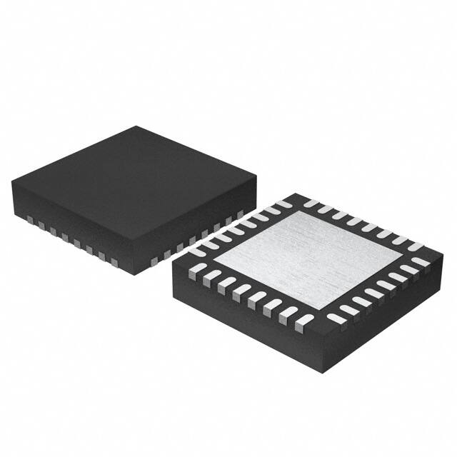
Small quad flat no-leads (QFN) package option
❐ 40% smaller than 20-pin TSSOP
❐ 22% smaller than 16-pin TSSOP
Meets most digital set top box, DVD recorder, and DTV
application requirements
■
Multiple high-performance PLLs allow synthesis of unrelated
frequencies
■
Selectable output frequency
■
■
Programmable output frequencies
Integration eliminates the need for external loop filter
components
■
Output frequency range:
❐ 1 MHz to 166 MHz
■
Meets critical timing requirements in complex system designs
■
Enables application compatibility
■
Input frequency range:
❐ Crystal: 10 MHz to 30 MHz
❐ External reference: 1 MHz to 100 MHz
■
Complete VCXO solution with ±120 ppm (typical pull range)
■
Analog voltage-control crystal oscillator (VCXO)
For a complete list of related documentation, click here.
■
16-/20-pin TSSOP and 32-pin QFN packages
■
3.3-V operation with 2.5-V output buffer option
Functional Description
Logic Block Diagram
FS0
FS1
FS2
Select
Logic
CLKA
PLL1
CLKB
CLKC
XIN
XOUT
PLL2
VCXO
Dividers
&
Multiplexers
VIN
PLL3
PLL4
CLKD
CLKE
CLKF
(CY22389 &
CY22391 only)
CLKG
(CY22389 &
CY22391 only)
CLKH
(CY22389 &
CY22391 only)
OE/PD#
(CY22389 &
CY22391 only)
Cypress Semiconductor Corporation
Document Number: 38-07734 Rev. *K
•
198 Champion Court
•
San Jose, CA 95134-1709
•
408-943-2600
Revised March 25, 2019
�CY22388
CY22389
CY22391
Contents
Pinouts .............................................................................. 3
Pin Definitions .................................................................. 4
General Description ......................................................... 5
Factory-Programmable CY22388/89/91 ...................... 5
PLLs ................................................................................... 5
Frequency Select Pin Operation ..................................... 5
Analog VCXO .................................................................... 6
VCXO Profile ..................................................................... 6
Absolute Maximum Conditions ....................................... 7
Pullable Crystal Specifications ....................................... 7
Operating Conditions ....................................................... 7
DC Parameters .................................................................. 8
AC Parameters .................................................................. 9
Test and Measurement ..................................................... 9
Voltage and Timing Definitions ..................................... 10
Document Number: 38-07734 Rev. *K
Ordering Information ...................................................... 11
Possible Configurations ............................................. 11
Ordering Code Definitions ......................................... 11
Package Drawing and Dimensions ............................... 12
Acronyms ........................................................................ 14
Document Conventions ................................................. 14
Units of Measure ....................................................... 14
Document History Page ................................................. 15
Sales, Solutions, and Legal Information ...................... 17
Worldwide Sales and Design Support ....................... 17
Products .................................................................... 17
PSoC® Solutions ...................................................... 17
Cypress Developer Community ................................. 17
Technical Support ..................................................... 17
Page 2 of 17
�CY22388
CY22389
CY22391
Pinouts
Figure 1. 16-pin TSSOP pinout
16-Pin TSSOP
XIN
1
16
XOUT
FS0
2
15
VDD
FS1
3
14
FS2
VIN
4
13
VDD
VDD
5
12
VSS
VSS
6
11
CLKE
CLKA
7
10
CLKD
CLKB
8
9
CLKC
CY22388
Figure 2. 20-pin TSSOP pinout
Figure 3. 32-pin QFN pinout
25 VDD
NC
28
26 VDD
NC
29
30 XIN
32 FS1
31 FS0
27 XOUT
32-Pin QFN
20- Pin TSSOP
XIN
1
20
XOUT
FS0
2
19
VDD
VIN
1
24 OE/PD#
FS1
3
18
OE/PD#
VDD
2
23
FS2
CLKH
4
17
FS2
VDD
3
22
VDD
VIN
VSS
4
21
VDD
VSS
5
20
VSS
VSS
6
19
VSS
VSS
7
18
CLKG
CLKH
8
17
CLKF
Document Number: 38-07734 Rev. *K
CLKE
VDD
CLKE
NC
11
15
10
16
CLKC
14
CLKF
13
CLKG
12
12
13
9
11
8
CLKA
9
CLKB
VSS
10
14
CLKC
VDD
7
CY22391
NC
16
CY22389
15
6
CLKA
CLKD
5
CLKB
VSS
CLKD
VDD
Page 3 of 17
�CY22388
CY22389
CY22391
Pin Definitions
Pin Name
Pin Number
Pin Description
16-pin TSSOP
20-pin TSSOP
32-pin QFN
XIN
1
1
30
XOUT
16
20
27
Crystal output (No connect if external clock is used)
CLKA
7
9
11
Clock output
CLKB
8
8
10
Clock output
CLKC
9
10
14
Clock output
CLKD
10
7
9
Clock output
CLKE
11
11
15
Clock output
CLKF
n/a
12
17
Clock output
CLKG
n/a
13
18
Clock output
CLKH
n/a
4
8
Clock output
2
2
31
Frequency select 0
FS0
Crystal input or reference clock input
FS1
3
3
32
Frequency select 1
FS2
14
17
23
Frequency select 2
OE/PD#
n/a
18
24
Programmable control pin: Output enable (active-high)
or power-down (active-low)
1
Analog control input for VCXO
VIN
4
16
VDD
5, 13, 15
5, 15, 19
VSS
6, 12
6, 14
NC
N/A
N/A
Document Number: 38-07734 Rev. *K
2, 3, 16, 21, 22, Voltage supply
25, 26
4, 5, 6, 7, 19, 20 Ground
12, 13, 28, 29
No connect.
Page 4 of 17
�CY22388
CY22389
CY22391
General Description
The CY22388 family of devices has an analog VCXO, four PLLs,
up to eight clock outputs and frequency selection capabilities.
The frequency selects do not modify any PLL frequency. Instead
they allow the user to choose among eight different output divider
selections depending on the clock and package configuration.
This is illustrated in Frequency Select Pin Operation.
There is one programmable OE/PD#. The OE/PD# pin can be
programmed as either an output enable pin or a power-down pin.
The OE function can be programmed to disable a selected set of
outputs when low, leaving the remaining outputs running.
Full-chip power-down disables all outputs and the PLLs and
most of the active circuitry when low.
Factory-Programmable CY22388/89/91
Factory programming is available for high- or low-volume
manufacturing by Cypress. All requests must be submitted to the
local Cypress field application engineer (FAE) or sales
representative. After the request is processed, you receive a new
part number, samples, and datasheet with the programmed
values. This part number is used for additional sample requests
and production orders.
To minimize parts per million (PPM) error on the clock outputs,
you must choose a crystal reference frequency that is a common
multiple of the desired PLL frequencies. While this is the ideal
situation, this is not always the case and the PLLs have
high-resolution counters internally to help minimize frequency
deviation from the desired frequency.
PLL VCO frequencies are generated by the following equation:
FVCO = FREF × (P / Q)
where FREF is the reference input frequency, P is the PLL
feedback divider, and Q is the reference input divider.
A PLL is a feedback system where the VCO frequency divided
by P and reference frequency divided by Q are constantly being
compared and the VCO frequency is adjusted to achieve a
locked state. Figure 4 is a simplified drawing of a PLL.
Figure 4. PLL system
F
R E F
/Q
V C O
a nd
Frequency Select Pin Operation
The advantage of having four PLLs is that a single device can
generate up to four independent frequencies from a single
crystal. Generally a design may require up to four oscillators to
accomplish what could be done with a single CY22388.
Table 1. CY22388 16-pin TSSOP
Each PLL is independent and can be configured to generate a
voltage-controlled oscillator (VCO) frequency between
62.5 MHz and 250 MHz. Each PLL can then, in turn, be divided
down with post dividers to generate the clock output frequency
of the user’s choice. The output divider allows each clock output
to be divided by 1, 2, 3, 4, 5, 6, 8, 9, 10, 12 or 15. The PLL
maximum is reduced to 166 MHz in ‘divide by 1’ mode due to
output buffer limitations.
CLK B
FS1, FS0
CLK C & CLK D
S0
CLK E
FIXED
Selected clock outputs are capable of being powered off a
separate 2.5-V supply. This allows for driving lower voltage swing
inputs. The CY22388/89/91 device still requires 3.3 V to power
the oscillator and all other internal PLL circuitry. For the 2.5-V
output option, refer to the CY22388 application note. Selected
clocks and pinout diagrams are explained in this application
note.
Clock D can obtain its output from either the reference source or
PLL1/N1 with N1 being defined as the output divider for PLL1.
Clock H is defined as a copy of clock D. Clock D is only available
from PLL1/N1 on the 16-pin package.
For CY22388, CLKB and CLKC have related frequencies. For
CY22389 and CY22391, CLKD and CLKF have related
frequencies, CLKA and CLKB have related frequencies, and
CLKC and CLKE have related frequencies. Related frequencies
come from the same PLL but can have different divider values.
Document Number: 38-07734 Rev. *K
V C O
/P
PLLs
Outputs that allow frequency switching perform a glitch-free
transition. A glitch is defined as a high- or low-time shorter than
half the smaller of the two periods being switched between.
Extended low time (even many cycles in duration) is acceptable.
F
O th e r
c o m p o n e n ts
Output Signal
CLK A
Frequency Selection Lines
FS2, FS1, FS0
Table 2. CY22389 20-pin TSSOP
Output Signal
CLK A
Frequency Selection Lines
FS2, FS1, FS0
CLK B & CLK C
FS1, FS0
CLK D, CLK E, & CLK F
FS0
CLK G
FIXED
CLK H
COPY OF CLK D
Table 3. CY22391 32-pin QFN
Output Signal
Frequency Selection Lines
CLK A
FS2, FS1, FS0
CLK B & CLK C
FS1, FS0
CLK D, CLK E, & CLK F
FS0
CLK G
FIXED
CLK H
COPY OF CLK D
Page 5 of 17
�CY22388
CY22389
CY22391
There are three programmable reference operating modes for
the CY22388, CY22389, and CY22391 family of devices. The
first mode uses an external pullable crystal and incorporates an
internal analog VCXO.
The second mode configures the internal crystal oscillator to
accept an external driven reference source from 1 to 100 MHz.
The input capacitance on the XIN PIN when driven in this mode
is 15 pF.
The third mode disables the VCXO input control and sets the
internal oscillator to a fixed frequency operation. The load
capacitance seen by the external crystal when connected to
PINS XIN and XOUT is equal to 12 pF.
One of the key components in the CY22388, CY22389, and
CY22391 family of devices is the analog VCXO. The VCXO is
used to ‘pull’ the reference crystal higher or lower to lock the
system frequency to an external source. This is ideal for
applications where the output frequency needs to track along
with an external reference frequency that is constantly shifting.
The VCXO is completely analog, so there is infinite resolution on
the VCXO pull curve. The analog to digital converter steps that
are normally associated with a digital VCXO input is not present
in this device. A special pullable crystal must be used in order to
Document Number: 38-07734 Rev. *K
have adequate VCXO pull range. Pullable crystal specifications
are included in this datasheet.
VCXO Profile
Figure 5 shows an example of what a VCXO profile looks like.
The analog voltage input is on the X-axis and the PPM range is
on the Y-axis. An increase in the VCXO input voltage results in a
corresponding increase in the output frequency. This has the
effect of moving the PPM from a negative to positive offset.
Figure 5. VCXO Profile
200
150
100
Tuning [ppm
Analog VCXO
50
0
-50
0
0.5
1
1.5
2
2.5
3
3.5
-100
-150
-200
VCXO input [V]
Page 6 of 17
�CY22388
CY22389
CY22391
Absolute Maximum Conditions
Parameter
Description
Condition
Min
Max
Unit
–0.5
4.6
V
Relative to VSS
–0.5
VDD + 0.5
VDC
Non-Functional
–65
125
°C
2000
–
V
10
ppm
VDD/AVDD/VDDL
Core supply voltage
VIN
Input voltage
TS
Temperature, Storage
ESDHBM
Electrostatic discharge (ESD)
protection (human body model)
MIL-STD-883, Method 3015
UL-94
Flammability rating
V-0 at 1/8 in.
MSL
Moisture sensitivity level
All packages
–
3
–
Pullable Crystal Specifications
Parameter [1, 2]
Description
Comments
FNOM
13.5-MHz and 27-MHz crystal
AT-Cut
Parallel resonance, fundamental
mode
CLNOM
Nominal load capacitance
Order crystal at one specific
CLNOM 0 ppm
R1
Equivalent series resistance
(ESR)
DL
Crystal drive level
C0[3]
Min
Typ
Max
Unit
See Note 2
11.4
12
12.6
pF
Fundamental mode (CL = Series)
–
–
40
Nominal VDD at 25 °C over
±120 ppm pull range
–
–
300
W
Crystal shunt capacitance
1.5
3
4.0
pF
C1[3]
Crystal motional capacitance
12
14
16.8
fF
F3SEPHI[2]
Third overtone separation from
3 × FNOM
Mechanical third (high side of
3 × FNOM)
240
–
–
ppm
F3SEPLO[2]
Third overtone separation from
3 × FNOM
Mechanical third (low side of
3 × FNOM)
–
–
–120
ppm
Operating Conditions
Min
Typ
Max
Unit
VDD/AVDD/VDDL
Parameter
Operating voltage
Description
3.0
3.3
3.6
V
TA
Ambient temperature
–10
–
70
°C
CLOAD
Maximum load capacitance
–
–
15
pF
tPU
Power-up time for all VDDs reach minimum specified voltage (power
ramps must be monotonic)
0.05
–
500
ms
Notes
1. Device operates to the following specs, which are guaranteed by design.
2. Refer to online software for a list of approved crystal specifications.
3. Increased tolerance available from pull range less than ±120 ppm.
Document Number: 38-07734 Rev. *K
Page 7 of 17
�CY22388
CY22389
CY22391
DC Parameters
Parameter [4]
Description
Conditions
Min
Typ
Max
Unit
Output high current
VOH = VDD – 0.5, VDD = 3.3 V
12
–
–
mA
IOL[5]
Output low current
VOL = 0.5, VDD = 3.3 V
12
–
–
mA
IIH
Input high current
VIH = VDD, excluding Vin, Xin
–
5
10
µA
IIL
Input low current
VIL = 0 V, excluding Vin, Xin
–
5
10
µA
VIH
Input high voltage
FS0/1/2 OE input CMOS levels
0.7 × AVDD
–
–
V
VIL
Input low voltage
FS0/1/2 OE input CMOS levels
–
–
0.3 × AVDD
V
VVCXO
VIN input range
Internal setting in VCXO are
XOB/A = 110, Offset = 1110,
Gain = 101
0
–
AVDD
V
CIN
Input capacitance
FS0/1/2 and OE pins only
–
–
7
pF
IVDD
Supply current
VDD/AVDD/VDDL current
–
60
–
mA
CINXIN
Input capacitance at XIN
VCXO disabled external reference
–
15
–
pF
CINXTAL
Input capacitance at crystal
VCXO disabled fixed frequency
oscillator
–
12
–
pF
IOH
[5]
Notes
4. Parameters are guaranteed by design and characterization. Not 100% tested in production. All parameters specified with fully loaded outputs.
5. Custom drive level is available upon request.
Document Number: 38-07734 Rev. *K
Page 8 of 17
�CY22388
CY22389
CY22391
AC Parameters
Parameter [4]
Min
Typ
Max
Units
1/t1
Output frequency
PLL minmax/Dividermaximum
Conditions
4.2
–
166
MHz
DC1
Output duty cycle
(excluding REFOUT
Duty cycle is defined in Figure 7;
t2/t1, 50% of VDD
External reference duty cycle
between 40% and 60% measured at
VDD/2 (Clock output is 125 MHz)
45
50
55
%
DC2
Output duty cycle
Duty cycle is defined in Figure 7;
t2/t1, 50% of VDD
External reference duty cycle
between 40% and 60% measured at
VDD/2 (Clock output is 125 MHz)
40
50
60
%
DCREFOUT
Output duty cycle
Duty cycle is defined in Figure 7;
t2/t1, 50% of VDD
(XIN Duty Cycle = 45/55%)
40
50
60
%
ER
Rising edge rate
Output clock edge rate. Measured
from 20% to 80% of VDD.
CLOAD = 15 pF. See Figure 8.
0.75
1.2
–
V/ns
EF
Falling edge rate
Output clock edge rate. Measured
from 80% to 20% of VDD.
CLOAD = 15 pF. See Figure 8.
0.75
1.2
–
V/ns
T9
Clock jitter
Period jitter
–
±250
–
ps
T10
PLL lock time
fXO
VCXO crystal pull range
Description
–
1
5
ms
Using non-SMD-49 crystal
Nominal crystal frequency input
assumed (0 ppm) at 25 °C and 3.3 V
±110
±120
–
ppm
Using SMD-49 crystal
Nominal crystal frequency input
assumed (0 ppm) at 25 °C and 3.3 V
±105
±120
–
ppm
Test and Measurement
Figure 6. Test and Measurement
V DDs
O utputs
DUT
0.1F
C LO A D
GND
Document Number: 38-07734 Rev. *K
Page 9 of 17
�CY22388
CY22389
CY22391
Voltage and Timing Definitions
Figure 7. Duty Cycle Definition
t1
t2
V DD
50% of V DD
Clock
Output
0V
Figure 8. ER = (0.6 VDD)/t3, EF = (0.6 VDD)/t4
t3
t4
V DD
80% of V DD
20% of V DD
Clock
Output
0V
Figure 9. FS Controlled Clock Output
Finish Cycle
Start at Full Cycle
FS
TWAIT
Document Number: 38-07734 Rev. *K
Page 10 of 17
�CY22388
CY22389
CY22391
Ordering Information
All product offerings are factory-programmed customer-specific devices with customized part numbers. The Possible Configurations
table shows the available device types, but not complete part numbers. Contact your local Cypress FAE or sales representative for
more information.
Part Number
Type
Package
Production Flow
Pb-free
CY22388FZXC
ZZ16
16-pin TSSOP
Commercial, 0 °C to +70 °C
CY22388FZXCT
ZZ16
16-pin TSSOP – Tape and Reel
Commercial, 0 °C to +70 °C
Possible Configurations
Part Number [6]
Type
Package
Production Flow
Pb-free
CY22388ZXC-xxx
ZZ16
16-pin TSSOP
Commercial, 0 °C to +70 °C
CY22388ZXC-xxxT
ZZ16
16-pin TSSOP – Tape and Reel
Commercial, 0 °C to +70 °C
CY22389ZXC-xxx
ZZ20
20-pin TSSOP
Commercial, 0 °C to +70 °C
CY22389ZXC-xxxT
ZZ20
20-pin TSSOP – Tape and Reel
Commercial, 0 °C to +70 °C
CY22391LTXC-xxx
LT32
32-pin QFN (Sawn)
Commercial, 0 °C to +70 °C
CY22391LTXC-xxxT
LT32
32-pin QFN (Sawn) – Tape and Reel
Commercial, 0 °C to +70 °C
Ordering Code Definitions
CY
223XX
XX X C - xxx
X
X = blank or T
blank = tube; T = Tape and Reel
Custom Configuration Code
Temperature Range: C = Commercial
Pb-free
Package: XX = Z or LT
Z = 16-pin TSSOP or 20-pin TSSOP
LT = 32-pin QFN
Part Identifier: 223XX = 22388 or 22389 or 22391
Company Code: CY = Cypress
Note
6. The CY22388ZXC-xxx, CY22389ZXC-xxx, and CY22391LTXC-xxx are factory-programmed configurations. For more details, contact your local Cypress FAE or
sales representative.
Document Number: 38-07734 Rev. *K
Page 11 of 17
�CY22388
CY22389
CY22391
Package Drawing and Dimensions
Figure 10. 16-pin TSSOP (4.40 mm Body) Package Outline, 51-85091
51-85091 *E
Figure 11. 20-pin TSSOP (4.40 mm Body) Package Outline, 51-85118
51-85118 *E
Document Number: 38-07734 Rev. *K
Page 12 of 17
�CY22388
CY22389
CY22391
Package Drawing and Dimensions (continued)
Figure 12. 32-pin QFN ((5 × 5 × 1.0 mm) 3.5 × 3.5 E-Pad (Sawn)) Package Outline, 001-30999
001-30999 *D
Document Number: 38-07734 Rev. *K
Page 13 of 17
�CY22388
CY22389
CY22391
Acronyms
Acronym
Document Conventions
Description
Units of Measure
ESD
Electrostatic Discharge
ESR
Equivalent Series Resistance
°C
degree Celsius
FAE
Field Application Engineer
fF
femtofarad
FS
Frequency Select
K
kilohm
PJ
Period Jitter
MHz
megahertz
PLL
Phase-Locked Loop
µA
microampere
QFN
Quad Flat No-leads
µF
microfarad
TSSOP
Thin Shrunk Small Outline Package
µs
microsecond
VCO
Voltage-Controlled Oscillator
µW
microwatt
VCXO
Voltage-Controlled Crystal Oscillator
mA
milliampere
ms
millisecond
mV
millivolt
ns
nanosecond
Document Number: 38-07734 Rev. *K
Symbol
Unit of Measure
ohm
PPM
parts per million
pF
picofarad
ps
picosecond
V
volt
W
watt
Page 14 of 17
�CY22388
CY22389
CY22391
Document History Page
Document Title: CY22388/CY22389/CY22391, Factory Programmable, Quad PLL Clock Generator with VCXO
Document Number: 38-07734
Revision
ECN
Orig. of
Change
Submission
Date
**
320458
RGL
03/07/2005
New data sheet.
*A
389649
RGL
08/02/2005
Updated Pullable Crystal Specifications:
Removed typical value of R1 parameter.
Changed maximum value of R1 parameter from 50 to 40 .
Updated details in “Comments” column corresponding to DL parameter.
Changed maximum value of DL parameter from 900 µW to 300 µW.
Updated AC Parameters:
Changed minimum value of fXO parameter from ±120 ppm to ±110 ppm.
Changed typical value of fXO parameter from blank to ±120 ppm.
*B
523597
RGL
11/12/2006
Updated AC Parameters:
Updated details in “Conditions” column corresponding to fXO parameter.
Retained existing values for fXO parameter corresponding to Test Condition
“Using non-SMD-49 crystal specified in “CY22388 Application Note,
ANC0002”.
Added values for fXO parameter corresponding to Test Condition “Using
SMD-49 crystal specified in “CY22388 Application Note, ANC0002”.
Updated to new template.
*C
2632357
KVM
01/13/2009
Updated Document Title to read as “CY22388, CY22389, CY22391 Factory
Programmable Quad PLL Clock Generator with VCXO”.
Updated Logic Block Diagram (Clarified that Power Down (PD#) is
active-low).
Updated Pinouts:
Updated Figure 2 (Replaced PD with PD#).
Updated Pin Definitions:
Replaced PD with PD#
Updated details in “Description” column corresponding to OE/PD# pin.
Updated DC Parameters:
Updated details in “Conditions” column corresponding to VVCXO parameter.
Updated Ordering Information:
Updated part numbers.
Added a column “Package” and added details in that column.
Added a Note “Not recommended for new designs. The LY32 QFN package
transitions to the LT32 QFN.” and referred the note in CY22391LFXC-xxx
and CY22391LFXC-xxxT.
Updated Package Drawing and Dimensions:
spec 51-85188 – Changed revision from *A to *B.
Updated to new template.
*D
2897246
KVM
03/22/2010
Updated Ordering Information:
Added description (Regarding Possible Configurations).
Updated Possible Configurations:
Updated part numbers.
Updated Note 6.
Removed Note “Not recommended for new designs. The LY32 QFN
package transitions to the LT32 QFN.”.
Updated Package Drawing and Dimensions:
51-85091 – Changed revision from *A to *B.
51-85118 – Changed revision from *A to *B.
001-30999 – Changed revision from *A to *C.
Removed spec 51-85188 *B.
Document Number: 38-07734 Rev. *K
Description of Change
Page 15 of 17
�CY22388
CY22389
CY22391
Document History Page (continued)
Document Title: CY22388/CY22389/CY22391, Factory Programmable, Quad PLL Clock Generator with VCXO
Document Number: 38-07734
Revision
ECN
Orig. of
Change
Submission
Date
*E
3030336
CXQ
09/14/2010
Fixed various typos across the document.
Updated Features:
Fixed formatting.
Updated Absolute Maximum Conditions:
Updated value of MSL parameter as 3 for all packages.
Updated Operating Conditions:
Removed “Recommended” from heading.
Updated Ordering Information:
No change in part numbers.
Added Ordering Code Definitions.
Updated Package Drawing and Dimensions:
spec 51-85091 – Changed revision from *B to *C.
spec 51-85118 – Changed revision from *B to *C.
Added Acronyms and Units of Measure.
Updated to new template.
*F
3786734
PURU
10/29/2012
Updated Pinouts:
Updated Figure 3 (Updated caption only).
Updated Ordering Information:
Updated part numbers (Added two part numbers (CY22388FZXC and
CY22388FZXCT)).
Updated Package Drawing and Dimensions:
spec 51-85091 – Changed revision from *C to *D.
spec 51-85118 – Changed revision from *C to *D.
spec 001-30999 – Changed revision from *C to *D.
*G
4142797
CINM
10/01/2013
Updated to new template.
Completing Sunset Review.
*H
4576237
CINM
11/21/2014
Updated Features:
Updated output frequency range as 1 MHz to 166 MHz.
Updated Functional Description:
Added “For a complete list of related documentation, click here.” at the end.
Updated Package Drawing and Dimensions:
spec 51-85091 – Changed revision from *D to *E.
spec 51-85118 – Changed revision from *D to *E.
*I
5475432
XHT
10/14/2016
Updated to new template.
Completing Sunset Review.
*J
5995535
AESATMP8
12/15/2017
Updated Cypress Logo and Copyright.
*K
6520812
XHT
03/25/2019
Updated Analog VCXO:
Updated description.
Updated Pullable Crystal Specifications:
Updated Note 2.
Updated AC Parameters:
Updated details in “Conditions” column corresponding to fXO parameter.
Updated to new template.
Document Number: 38-07734 Rev. *K
Description of Change
Page 16 of 17
�CY22388
CY22389
CY22391
Sales, Solutions, and Legal Information
Worldwide Sales and Design Support
Cypress maintains a worldwide network of offices, solution centers, manufacturer’s representatives, and distributors. To find the office
closest to you, visit us at Cypress Locations.
PSoC® Solutions
Products
Arm® Cortex® Microcontrollers
Automotive
cypress.com/arm
cypress.com/automotive
Clocks & Buffers
Interface
Internet of Things
Memory
cypress.com/clocks
cypress.com/interface
cypress.com/iot
cypress.com/memory
Microcontrollers
cypress.com/mcu
PSoC
cypress.com/psoc
Power Management ICs
Touch Sensing
USB Controllers
Wireless Connectivity
PSoC 1 | PSoC 3 | PSoC 4 | PSoC 5LP | PSoC 6 MCU
Cypress Developer Community
Community | Projects | Video | Blogs | Training | Components
Technical Support
cypress.com/support
cypress.com/pmic
cypress.com/touch
cypress.com/usb
cypress.com/wireless
© Cypress Semiconductor Corporation, 2005–2019. This document is the property of Cypress Semiconductor Corporation and its subsidiaries (“Cypress”). This document, including any software or
firmware included or referenced in this document (“Software”), is owned by Cypress under the intellectual property laws and treaties of the United States and other countries worldwide. Cypress
reserves all rights under such laws and treaties and does not, except as specifically stated in this paragraph, grant any license under its patents, copyrights, trademarks, or other intellectual property
rights. If the Software is not accompanied by a license agreement and you do not otherwise have a written agreement with Cypress governing the use of the Software, then Cypress hereby grants
you a personal, non-exclusive, nontransferable license (without the right to sublicense) (1) under its copyright rights in the Software (a) for Software provided in source code form, to modify and reproduce
the Software solely for use with Cypress hardware products, only internally within your organization, and (b) to distribute the Software in binary code form externally to end users (either directly or
indirectly through resellers and distributors), solely for use on Cypress hardware product units, and (2) under those claims of Cypress’s patents that are infringed by the Software (as provided by
Cypress, unmodified) to make, use, distribute, and import the Software solely for use with Cypress hardware products. Any other use, reproduction, modification, translation, or compilation of the
Software is prohibited.
TO THE EXTENT PERMITTED BY APPLICABLE LAW, CYPRESS MAKES NO WARRANTY OF ANY KIND, EXPRESS OR IMPLIED, WITH REGARD TO THIS DOCUMENT OR ANY SOFTWARE
OR ACCOMPANYING HARDWARE, INCLUDING, BUT NOT LIMITED TO, THE IMPLIED WARRANTIES OF MERCHANTABILITY AND FITNESS FOR A PARTICULAR PURPOSE. No computing
device can be absolutely secure. Therefore, despite security measures implemented in Cypress hardware or software products, Cypress shall have no liability arising out of any security breach, such
as unauthorized access to or use of a Cypress product. CYPRESS DOES NOT REPRESENT, WARRANT, OR GUARANTEE THAT CYPRESS PRODUCTS, OR SYSTEMS CREATED USING
CYPRESS PRODUCTS, WILL BE FREE FROM CORRUPTION, ATTACK, VIRUSES, INTERFERENCE, HACKING, DATA LOSS OR THEFT, OR OTHER SECURITY INTRUSION (collectively, “Security
Breach”). Cypress disclaims any liability relating to any Security Breach, and you shall and hereby do release Cypress from any claim, damage, or other liability arising from any Security Breach. In
addition, the products described in these materials may contain design defects or errors known as errata which may cause the product to deviate from published specifications. To the extent permitted
by applicable law, Cypress reserves the right to make changes to this document without further notice. Cypress does not assume any liability arising out of the application or use of any product or
circuit described in this document. Any information provided in this document, including any sample design information or programming code, is provided only for reference purposes. It is the
responsibility of the user of this document to properly design, program, and test the functionality and safety of any application made of this information and any resulting product. “High-Risk Device”
means any device or system whose failure could cause personal injury, death, or property damage. Examples of High-Risk Devices are weapons, nuclear installations, surgical implants, and other
medical devices. “Critical Component” means any component of a High-Risk Device whose failure to perform can be reasonably expected to cause, directly or indirectly, the failure of the High-Risk
Device, or to affect its safety or effectiveness. Cypress is not liable, in whole or in part, and you shall and hereby do release Cypress from any claim, damage, or other liability arising from any use of
a Cypress product as a Critical Component in a High-Risk Device. You shall indemnify and hold Cypress, its directors, officers, employees, agents, affiliates, distributors, and assigns harmless from
and against all claims, costs, damages, and expenses, arising out of any claim, including claims for product liability, personal injury or death, or property damage arising from any use of a Cypress
product as a Critical Component in a High-Risk Device. Cypress products are not intended or authorized for use as a Critical Component in any High-Risk Device except to the limited extent that (i)
Cypress’s published data sheet for the product explicitly states Cypress has qualified the product for use in a specific High-Risk Device, or (ii) Cypress has given you advance written authorization to
use the product as a Critical Component in the specific High-Risk Device and you have signed a separate indemnification agreement.
Cypress, the Cypress logo, Spansion, the Spansion logo, and combinations thereof, WICED, PSoC, CapSense, EZ-USB, F-RAM, and Traveo are trademarks or registered trademarks of Cypress in
the United States and other countries. For a more complete list of Cypress trademarks, visit cypress.com. Other names and brands may be claimed as property of their respective owners.
Document Number: 38-07734 Rev. *K
Revised March 25, 2019
Page 17 of 17
�


 工商网监
湘ICP备2023018690号
工商网监
湘ICP备2023018690号
