THIS SPEC IS OBSOLETE
Spec No: 001-66175
Spec Title: CY22391-09, PLL CLOCK GENERATOR
Replaced by: NONE
�CY22391-09
PLL Clock Generator
PLL Clock Generator
Features
Functional Description
■
Input: 24.576 MHz clock reference
The CY22391-09 is a PLL-based clock generator that uses an
externally generated 24.576-MHz clock reference to generate
six clock outputs. The 27-MHz outputs and the 24-MHz output
can be disabled using the input select pins as described in
Frequency and Function Table on page 4. The device operates
at 3.3 V.
■
Outputs:
❐ 27 MHz clock × 3 with on/off function
❐ 24 MHz clock with on/off function
❐ 16 MHz clock
❐ 25 MHz clock
■
Supply voltage: 3.3 V
■
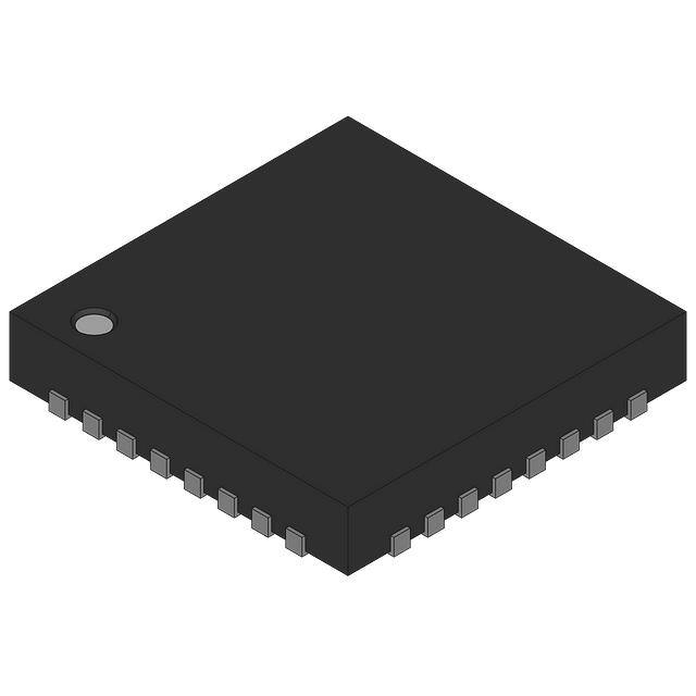
Package: Pb-free 32-pin 5 mm × 5 mm quad flat no-leads (QFN)
■
Temperature range: Commercial
Logic Block Diagram
AVDD
XIN
clock
buffer
VDD_A
27M-1
27M-2
PLL Clock
Synthesizer
27M-3
Dividers, Buffers
and
Configuration
Logic
OE
FS0
VDD_B
16M
24M
25M
AVSS, VSS_A, VSS_B
Cypress Semiconductor Corporation
Document Number: 001-66175 Rev. *B
•
198 Champion Court
•
San Jose, CA 95134-1709
•
408-943-2600
Revised February 22, 2017
�CY22391-09
Contents
Pin Configuration ............................................................. 3
Pin Definitions .................................................................. 3
Output Frequencies .......................................................... 4
Frequency and Function Table .................................... 4
Multiple Power Supply ..................................................... 4
Absolute Maximum Conditions ....................................... 5
DC Electrical Specifications ............................................ 5
AC Electrical Specifications ............................................ 6
Input Clock (24.576 MHz) Specifications ........................ 6
Switching Waveforms ...................................................... 7
Ordering Information ........................................................ 9
Ordering Code Definitions ........................................... 9
Document Number: 001-66175 Rev. *B
Package Diagram ............................................................ 10
Acronyms ........................................................................ 11
Document Conventions ................................................. 11
Units of Measure ....................................................... 11
Document History Page ................................................. 12
Sales, Solutions, and Legal Information ...................... 13
Worldwide Sales and Design Support ....................... 13
Products .................................................................... 13
PSoC® Solutions ...................................................... 13
Cypress Developer Community ................................. 13
Technical Support ..................................................... 13
Page 2 of 13
�CY22391-09
Pin Configuration
AVDD
AVDD
NC
XOUT
NC
FS0
XIN
FS1
Figure 1. 32-pin QFN pinout
32 31 30 29 28 27 26 25
VIN
24 OE
1
VDD_A 2
23 FS2
VDD_A 3
22 VDD_B
AVSS 4
21 VDD_B
AVSS 5
20 VSS_B
VSS_A 6
19 VSS_B
VSS_A 7
18 DNU
17 25M
27M-2 8
24M
VDD_B
16M
NC
NC
27M-1
DNU
27M-3
9 10 11 12 13 14 15 16
Pin Definitions
Pin No.
Name
I/O
1
VIN
Input
2, 3
VDD_A
Power
Description
Unused Input, connect to VDD or VSS
Power supply for 27M-1, 27M-2, and 27M-3 outputs: 3.3 V
4, 5
AVSS
Power
Analog supply ground
6, 7
VSS_A
Power
Power supply ground
8
27M-2
Output
27 MHz clock output, On/Off controlled by OE
9
27M-3
Output
27 MHz clock output, On/Off controlled by FS0
10
DNU
Output
Unused output, leave floating
11
27M-1
Output
27 MHz clock output, On/Off controlled by OE
12,13
14
NC
No connect
16M
Output
16 MHz clock output
15
24M
Output
24 MHz clock output, On/Off controlled by OE
16
VDD_B
Power
Power supply for 16M, 24M, and 25M outputs: 3.3 V
17
25M
Output
25 MHz clock output
18
DNU
Output
Unused output, leave floating
19, 20
VSS_B
Power
Power supply ground
21, 22
VDD_B
Power
Power supply for 16M, 24M, and 25M outputs: 3.3 V
23
FS2
Input
Unused input. Connect to VDD or VSS
24
OE
Input
Output on/off control for 27M-1, 27M-2 and 24M. See Frequency and Function Table on page 4.
25, 26
AVDD
Power
Analog (Core) power supply: 3.3 V
27
XOUT
Output
Crystal reference output, leave floating
28, 29
30
NC
XIN
No connect
Input
Clock reference input, 24.576 MHz
31
FS0
Input
Output on/off control for 27M-3. See Frequency and Function Table on page 4.
32
FS1
Input
Unused input. Connect to VDD or VSS
Document Number: 001-66175 Rev. *B
Page 3 of 13
�CY22391-09
Output Frequencies
Frequency and Function Table
Input
Output (MHz)
FS0
OE
27M-1
27M-2
0
0
Low
Low
0
1
27.00
27.00
27M-3
16M
24M
25M
Low
16
Low
25
Low
16
24
25
1
0
Low
Low
27.00
16
Low
25
1
1
27.00
27.00
27.00
16
24
25
Multiple Power Supply
The second power supply, VDD_A, supplies power for the output
drivers at pins 8, 9, and 11.
The CY22391-09 has three groups of power supplies: AVDD,
VDD_A, and VDD_B. All supplies are 3.3 V.
The third power supply, VDD_B, supplies power for the output
drivers at pins 14, 15 and 17.
AVDD supplies power to the internal core (PLLs) and the control
circuitry. AVDD must have low noise because noise on AVDD
may degrade the PLL performance.
There is no power supply sequencing required between these
three supplies. However, the AVDD ramp must be monotonic as
described in DC Electrical Specifications on page 5.
Document Number: 001-66175 Rev. *B
Page 4 of 13
�CY22391-09
Absolute Maximum Conditions
Exceeding maximum ratings may shorten the useful life of the device. User guidelines are not tested.
Min
Max
Unit
VAVDD
Parameter
AVDD (Core) supply voltage
Description
Condition
–0.5
4.6
V
VDDA
VDD_A supply voltage
–0.5
4.6
V
VDDB
VDD_B supply voltage
–0.5
4.6
V
VIN
Input voltage
Relative to VSS
–0.5
VDD + 0.5
V
TS
Temperature, Storage
Non-functional
–65
150
°C
TA
Temperature, Operating ambient Functional
0
85
°C
TJ
Temperature, Junction
Functional
–
150
°C
ØJC
Dissipation, Junction to case
Mil-Spec 883E Method 1012.1
–
23
°C/W
ESDHBM
Electrostatic discharge (ESD)
protection (human body model)
JEDEC STD 22-A114-B
2000
–
V
UL-94
Flammability rating
At 1/8 in.
MSL
Moisture sensitivity level
V–0
3
Multiple Supplies: The voltage on any input or I/O pin cannot exceed the power pin during power-up. Power supply sequencing is not required.
DC Electrical Specifications
Parameter [1]
Min
Max
Unit
VAVDD
AVDD (Core) operating voltage
Description
3.3 V typical
Condition
3.0
3.6
V
VDDA
VDD_A operating voltage
3.3 V typical
3.0
3.6
V
VDDB
VDD_B operating voltage
3.3 V typical
3.0
3.6
V
VIL
Input low voltage
All inputs
–
0.3 × AVDD
V
VIH
Input high voltage
All inputs
0.7 × AVDD
–
V
VOH
Output high voltage
IOH = –2 mA
0.8 × VDD
–
V
VOL
Output low voltage
IOL = 2 mA
–
0.2 × VDD
V
CIN
Input pin capacitance
All inputs
2
5
pF
IDD
Dynamic supply current
At max load and frequency
–
80
mA
tPU
Power-up time for all VDDs
Power-up to reach minimum specified voltage
(power ramp must be monotonic). See Figure 7
on page 7.
0.05
500
ms
Note
1. Parameters are guaranteed by design and characterization. Not 100% tested in production. All parameters specified with fully loaded outputs.
Document Number: 001-66175 Rev. *B
Page 5 of 13
�CY22391-09
AC Electrical Specifications
Parameter [2]
Description
Condition
Min
Typ
Max
Unit
27M-1, -2, -3
DC27
27 MHz output duty cycle
CLOAD = 15 pF, See Figure 4 on page 7
45
50
55
%
ER
Rising edge rate
CLOAD = 15 pF, See Figure 5 on page 7
0.7
1.2
–
V/ns
EF
Falling edge rate
CLOAD = 15 pF, See Figure 5 on page 7
0.7
1.2
–
V/ns
tPJ
27M-1, -2, -3 period jitter
Over 10K cycle, See Figure 6 on page 7
–
170
350
ps
tLTJ
27 MHz long term jitter
at 20 s, using 420 ps Long term Source
–
500
900
ps
DC16
16 MHz output duty cycle
CLOAD = 15 pF, See Figure 4 on page 7
45
50
55
%
ER
Rising edge rate
CLOAD = 15 pF, See Figure 5 on page 7
0.7
1.2
–
V/ns
EF
Falling edge rate
CLOAD = 15 pF, See Figure 5 on page 7
0.7
1.2
–
V/ns
tPJ
16M period jitter
Over 10 K cycle, See Figure 6 on page 7
–
220
425
ps
tLTJ
16 MHz long term jitter
at 20 s, using 420 ps Long term Source
–
500
750
ps
DC24
24 MHz output duty cycle
CLOAD = 15 pF, See Figure 4 on page 7
45
50
55
%
ER
Rising edge rate
CLOAD = 15 pF, See Figure 5 on page 7
0.7
1.2
–
V/ns
EF
Falling edge rate
CLOAD = 15 pF, See Figure 5 on page 7
0.7
1.2
–
V/ns
tPJ
24M period jitter
Over 10 K cycle, See Figure 6 on page 7
–
180
300
ps
tLTJ
24 MHz long term jitter
at 20 s, using 420 ps Long term Source
–
500
750
ps
DC25
25 MHz output duty cycle
CLOAD = 15 pF, See Figure 4 on page 7
45
50
55
%
ER
Rising edge rate
CLOAD = 15 pF, See Figure 5 on page 7
0.7
1.2
–
V/ns
EF
Falling edge rate
CLOAD = 15 pF, See Figure 5 on page 7
0.7
1.2
–
V/ns
tPJ
25 MHz period jitter
Over 10 K cycle, See Figure 6 on page 7
–
160
350
ps
tLTJ
25 MHz long term jitter
At 20 s, using 420 ps long-term source
–
600
900
ps
See Figure 7 on page 7.
Time from AVDD reaches at minimum
specified level and clock applied
–
1
5
ms
16M
24M
25M
Enable/Disable and Start-up
tLOCK
PLL lock time
Input Clock (24.576 MHz) Specifications
Parameter
Description
Condition
Min
Typ
Max
Unit
40
50
60
%
DC
Input clock duty cycle
VIH
Input high voltage
0.7 AVDD
–
–
V
VIL
Input low voltage
–
–
0.2 AVDD
V
TR/TF[3]
Rise/Fall time
–
–
5
ns
Between 30–70% of AVDD
Notes
2. Parameters are guaranteed by design and characterization. Not 100% tested in production. All parameters specified with fully loaded outputs.
3. Excessive noise on the input clock may degrade long term jitter performance.
Document Number: 001-66175 Rev. *B
Page 6 of 13
�CY22391-09
Switching Waveforms
Figure 2. Long term jitter
tLTJ
More than 20s
50% of VDD
CLOCK
Figure 3. Output Test Load
Measurement
Point
CLOAD
Figure 4. Duty Cycle Definition: DC = t1 / t2
t1
50% of VDD
CLOCK
t2
Figure 5. Edge Rate Definition: ER = 0.6 × VDD / t3, EF = 0.6 × VDD / t4
t4
t3
80% of VDD
20% of VDD
CLOCK
Figure 6. Period Jitter: tPJ = tMAX – tMIN (over 10,000 Cycles)
tMAX
tMIN
50% of VDD
CLOCK
Figure 7. Power up and Lock Time
VDD(Min.)
VDD
Output Stable
Output
tPU
Document Number: 001-66175 Rev. *B
tLOCK
Page 7 of 13
�CY22391-09
Switching Waveforms (continued)
Figure 8. Sample 24.576 MHz Input Long Term Jitter vs. 27 MHz Output Long term Jitter (Information Only)
Output Long Term Jitter (ps)
1600
1400
1200
1000
800
600
400
200
200
400
600
800
1000
1200
1400
Input Long Term Jitter (ps)
Document Number: 001-66175 Rev. *B
Page 8 of 13
�CY22391-09
Ordering Information
Part Number
Package Type
Product Flow
Pb-free
CY22391LTXC-09
32-pin QFN
Commercial, 0 °C to 85 °C
CY22391LTXC-09T
32-pin QFN – Tape and Reel
Commercial, 0 °C to 85 °C
Ordering Code Definitions
CY 22391 LT X C
xx
X
X = blank or T
blank = Tube; T = Tape and Reel
Part configuration code: xx = 09
Temperature Range:
C = Commercial
Pb-free
Package Type: LT = 32-pin QFN
Base part number
Company ID: CY = Cypress
Document Number: 001-66175 Rev. *B
Page 9 of 13
�CY22391-09
Package Diagram
Figure 9. 32-pin QFN (5 × 5 × 1.0 mm) 3.5 × 3.5 E-Pad (Sawn) Package Outline, 001-30999
001-30999 *D
Document Number: 001-66175 Rev. *B
Page 10 of 13
�CY22391-09
Acronyms
Acronym
Document Conventions
Description
Units of Measure
CCJ
Cycle-to-Cycle Jitter
DNU
Do Not Use
A
ampere
DUT
Device Under Test
°C
degree Celsius
EMI
Electromagnetic Interference
dB
decibel
ESD
Electrostatic Discharge
fF
femtofarad
FAE
Field Application Engineer
KB
kilobyte
FS
Frequency Select
Kbit
kilobit
LTJ
Long Term Jitter
KHz
kilohertz
OE
Output Enable
K
kilohm
PJ
Period Jitter
MHz
megahertz
PLL
Phase Locked Loop
M
megaohm
QFN
Quad Flat No-leads
mA
milliampere
ms
millisecond
mV
millivolt
nA
nanoampere
ns
nanosecond
nV
nanovolt
ohm
ppm
parts per million
pA
picoampere
pF
picofarad
ps
picosecond
V
volt
W
watt
Document Number: 001-66175 Rev. *B
Symbol
Unit of Measure
Page 11 of 13
�CY22391-09
Document History Page
Document Title: CY22391-09, PLL Clock Generator
Document Number: 001-66175
Rev.
ECN No.
Submission
Date
Orig. of
Change
Description of Change
**
3121675
01/06/2011
XHT
New data sheet.
*A
4267285
01/30/2014
CINM
Updated Package Diagram:
spec 001-30999 – Changed revision from *C to *D.
Updated to new template.
Completing Sunset Review.
*B
5639818
02/22/2017
PAWK
Obsolete document.
Completing Sunset Review.
Document Number: 001-66175 Rev. *B
Page 12 of 13
�CY22391-09
Sales, Solutions, and Legal Information
Worldwide Sales and Design Support
Cypress maintains a worldwide network of offices, solution centers, manufacturer’s representatives, and distributors. To find the office
closest to you, visit us at Cypress Locations.
PSoC® Solutions
Products
Automotive
Clocks & Buffers
Interface
Lighting & Power Control
cypress.com/go/automotive
cypress.com/go/clocks
cypress.com/go/interface
cypress.com/go/powerpsoc
cypress.com/go/plc
Memory
PSoC
Touch Sensing
cypress.com/go/memory
cypress.com/go/psoc
PSoC 1 | PSoC 3 | PSoC 4 | PSoC 5LP
Cypress Developer Community
Community | Forums | Blogs | Video | Training
Technical Support
cypress.com/go/support
cypress.com/go/touch
USB Controllers
Wireless/RF
psoc.cypress.com/solutions
cypress.com/go/USB
cypress.com/go/wireless
© Cypress Semiconductor Corporation, 2011-2017. The information contained herein is subject to change without notice. Cypress Semiconductor Corporation assumes no responsibility for the use of
any circuitry other than circuitry embodied in a Cypress product. Nor does it convey or imply any license under patent or other rights. Cypress products are not warranted nor intended to be used for
medical, life support, life saving, critical control or safety applications, unless pursuant to an express written agreement with Cypress. Furthermore, Cypress does not authorize its products for use as
critical components in life-support systems where a malfunction or failure may reasonably be expected to result in significant injury to the user. The inclusion of Cypress products in life-support systems
application implies that the manufacturer assumes all risk of such use and in doing so indemnifies Cypress against all charges.
Any Source Code (software and/or firmware) is owned by Cypress Semiconductor Corporation (Cypress) and is protected by and subject to worldwide patent protection (United States and foreign),
United States copyright laws and international treaty provisions. Cypress hereby grants to licensee a personal, non-exclusive, non-transferable license to copy, use, modify, create derivative works of,
and compile the Cypress Source Code and derivative works for the sole purpose of creating custom software and or firmware in support of licensee product to be used only in conjunction with a Cypress
integrated circuit as specified in the applicable agreement. Any reproduction, modification, translation, compilation, or representation of this Source Code except as specified above is prohibited without
the express written permission of Cypress.
Disclaimer: CYPRESS MAKES NO WARRANTY OF ANY KIND, EXPRESS OR IMPLIED, WITH REGARD TO THIS MATERIAL, INCLUDING, BUT NOT LIMITED TO, THE IMPLIED WARRANTIES
OF MERCHANTABILITY AND FITNESS FOR A PARTICULAR PURPOSE. Cypress reserves the right to make changes without further notice to the materials described herein. Cypress does not
assume any liability arising out of the application or use of any product or circuit described herein. Cypress does not authorize its products for use as critical components in life-support systems where
a malfunction or failure may reasonably be expected to result in significant injury to the user. The inclusion of Cypress’ product in a life-support systems application implies that the manufacturer
assumes all risk of such use and in doing so indemnifies Cypress against all charges.
Use may be limited by and subject to the applicable Cypress software license agreement.
Document Number: 001-66175 Rev. *B
Revised February 22, 2017
All products and company names mentioned in this document may be the trademarks of their respective holders.
Page 13 of 13
�