UniClock CY22U1
Single Output, Low Power Programmable
Clock Generator
Single Output, Low Power Programmable Clock Generator
Features
Benefits
■
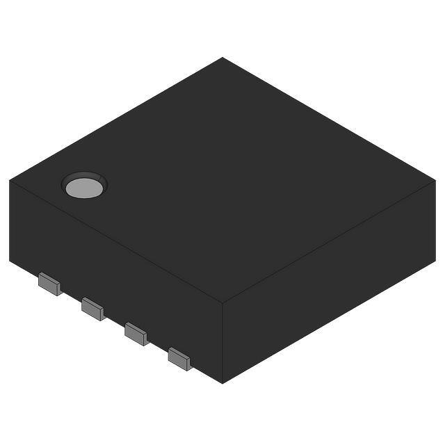
Small Footprint, 8-pin QFN 1.7 mm × 1.7 mm × 0.6 mm package
■
Low Power and Low Jitter Operation
■
Multiple Operating Voltages:
❐ CY22U1S: 2.5 V, 3.0 V, or 3.3 V
❐ CY22U1L: 1.8 V
■
Programmable Single Output Clock Generator Frequency
Range:
❐ 1 to 200 MHz
■
Crystal or External Reference Clock Input Frequency Range:
❐ Fundamental Tuned Crystal: 8 to 48 MHz
❐ External Reference Clock: 1 to 166 MHz
■
Programmable Capacitor Tuning Array
■
Programmable PD# or OE Control Pin
■
Programmable Asynchronous or Synchronous OE and PD#
Modes
■
Services digital televisions and displays, set top boxes,
multifunction printers, and a variety of consumer electronics
applications.
■
Saves PCB space due to small form factor.
■
Enables quick turnaround and flexibility and adaptability to
design changes through programmability.
■
Enables synthesis of highly accurate and stable output clock
frequencies with zero or low ppm error.
■
Enables fine tuning of output clock frequency by adjusting the
crystal load CLoad using programmable internal capacitors.
■
Lowers clock solution cost by pairing a high frequency PLL
programmability with a low cost, low frequency crystal.
■
Enables low power during the power down or output disable
function.
■
Provides flexibility for system applications through selectable
asynchronous or synchronous output enable and disable.
Logic Block Diagram
Cypress Semiconductor Corporation
Document Number: 001-50320 Rev. *E
•
198 Champion Court
•
San Jose, CA 95134-1709
•
408-943-2600
Revised December 20, 2012
�UniClock CY22U1
Contents
Pinouts .............................................................................. 3
Pin Definitions .................................................................. 3
Functional Description ..................................................... 3
Configurable PLL ......................................................... 3
Input Reference Clock Option ..................................... 3
Multiple VDD Power Supply Option ............................. 4
Power Management Feature ....................................... 4
Crystal Oscillator Tuning Circuit .................................... 4
Programmable Features .................................................. 5
Programming Support ..................................................... 5
Absolute Maximum Ratings ............................................ 5
Recommended Operating Conditions ............................ 5
DC Electrical Specifications ............................................ 6
AC Electrical Specifications ............................................ 7
Recommended Crystal Specifications
for SMD Package .............................................................. 7
Document Number: 001-50320 Rev. *E
Switching Waveforms ...................................................... 8
Ordering Information ...................................................... 10
Possible Configurations ............................................. 10
Ordering Code Definitions ......................................... 10
Package Drawing and Dimensions ............................... 12
Acronyms ........................................................................ 13
Document Conventions ................................................. 13
Units of Measure ....................................................... 13
Document History Page ................................................. 14
Sales, Solutions, and Legal Information ...................... 15
Worldwide Sales and Design Support ....................... 15
Products .................................................................... 15
PSoC Solutions ......................................................... 15
Page 2 of 15
�UniClock CY22U1
Pinouts
VDD
NC
Figure 1. Pin Diagram – CY22U1 8-pin 1.7 mm × 1.7 mm QFN
8
7
XOUT 1
6
CLKOUT
5
NC
CY22U1
3
4
GND
2
PD#/OE
XIN/CLKIN
Pin Definitions
CY22U1 8-pin 1.7 mm × 1.7 mm QFN
Pin Number
Name
IO
Output
Description
1
XOUT
2
XIN/CLKIN
Input
Crystal or external clock input.
3
PD#/OE
Input
Multifunction pin. Active low power down or active high output enable pin. Has weak
internal pull up.
4
GND
5
NC
6
CLKOUT
7
NC
8
VDD
Power
–
Output
–
Power
Crystal output. Float for external clock input.
Power supply ground.
No connect. Pin has no internal connection.
Programmable clock output. Output voltage depends on VDD. Has weak internal pull
down.
No connect. Pin has no internal connection.
Programmable power supply:
CY22U1S: 2.5 V, 3.0 V, 3.3 V (standard voltage)
CY22U1L: 1.8 V (low voltage)
Functional Description
The UniClock CY22U1 is a programmable, high accuracy,
PLL-based clock generator device designed to replace crystals
and crystal oscillators and save on cost and board space, while
increasing reliability. The low jitter and accurate outputs makes
this device suitable for use in digital televisions and displays, set
top boxes, multifunction printers, and a variety of consumer
electronics applications.
The device has several programmable options listed in the
section Programmable Features on page 5. The entire
configuration is one time programmable.
Document Number: 001-50320 Rev. *E
Configurable PLL
The device uses a programmable PLL to generate output
frequencies from 1 to 200 MHz. The high resolution of the PLL
and flexible output dividers provide this flexibility.
Input Reference Clock Option
There is an option of a crystal or clock signal for the input
reference clock. The frequency range for crystal (XIN) is 8 MHz
to 48 MHz, while the range for an external reference clock
(CLKIN) is 1 MHz to 166 MHz. A PLL bypass mode enables this
device to be used as a crystal oscillator.
Page 3 of 15
�UniClock CY22U1
Multiple VDD Power Supply Option
be a full clock when exiting power down in synchronous or
asynchronous mode.
The device has programmable power supply options. The
operating supply voltages are 2.5 V, 3.0 V, or 3.3 V for CY22U1S
and 1.8 V for CY22U1L.
Output Frequency Tuning
The UniClock CY22U1 contains an on-chip oscillator with a built
in programmable capacitor array for fine tuning of the output
frequency. The capacitive load seen by the crystal is adjusted by
programming the memory bits. This feature can compensate for
crystal variations or provide a more accurate synthesized
frequency. Figure 2 shows the crystal oscillator tuning circuit
block diagram.
Power Management Feature
The UniClock CY22U1 offers PD# (active LOW) and OE (active
HIGH) functions. When the power down mode is selected
(PD# = 0), the oscillator and PLL are placed in a low supply
current standby mode and the output is tristated and weakly
pulled LOW. The oscillator and PLL circuits must relock when the
part exits the power down mode. If the output is disabled
(OE = 0), the output is tristated and weakly pulled LOW. In this
mode, the oscillator and PLL circuits continue to operate, which
enables a rapid return to normal operation when the output is
enabled.
Crystal Oscillator Tuning Circuit
Table 1. Crystal Oscillator Tuning Capacitor Values
Cap
Value [1]
Unit
C7
5.000
pF
C6
2.500
pF
C5
1.250
pF
C4
0.625
pF
C3
0.313
pF
C2
0.156
pF
C1
0.078
pF
C0
0.039
pF
In addition, the PD# or OE mode can be programmed to occur
asynchronously or synchronously with respect to the output
signal. When the asynchronous setting is used, entering power
down or disabling the output occurs immediately (enabling logic
delays), regardless of the position in the clock cycle. Similarly,
exiting power down or enabling the output occurs immediately
with no guarantee of full output clock pulses. However, when the
synchronous setting is used, the part waits for a falling edge at
the output before entering power down or disabling the output.
This prevents output glitches. The first output pulse is
guaranteed to be a full clock pulse when enabling outputs with a
synchronous OE pin. The first output pulse is not guaranteed to
Figure 2. Crystal Oscillator Tuning Block Diagram
FXIN, ESR, C0
RF
-R
CPXIN
CXIN
C1
C0
X0
C2
X1
C3
X2
C4
X3
C5
X4
C6
X5
C7
X6
C7
X7
X7
C5
C6
X6
X5
C4
X4
C3
X3
C2
X2
C1
X1
C0
CXOUT
CPXOUT
X0
Note
1. The capacitor values are nominal.
Document Number: 001-50320 Rev. *E
Page 4 of 15
�UniClock CY22U1
Programmable Features
Programming Support
The following list of features can be custom configured:
The device is available in factory and field programmable
versions.
The
CyClockMaker
Programming
kit
(CY3675-CLKMAKER1)
along
with
CyClockWizard
configuration software is used for field programming the device.
For specific programming needs, contact your local Cypress field
application engineer (FAE) or sales representative.
■
PLL frequency and output divider value
■
Oscillator tuning (crystal load) capacitance value
■
Direct oscillator output (PLL bypass)
■
High or low power supply voltage operation
■
Power management mode (OE or PD#)
■
Power management timing (synchronous or asynchronous)
Absolute Maximum Ratings
Exceeding maximum ratings may shorten the useful life of the device. User guidelines are not tested.
Table 2. Absolute Maximum Ratings
Parameter [2]
VDD
Description
Condition
Min
Max
Unit
Supply voltage, 2.5 V/3.0 V/3.3 V range
–0.5
4.4
V
Supply voltage, 1.8 V range
–0.5
2.8
V
VIN
Input voltage
Relative to VSS
–0.5
VDD + 0.5
V
TS
Temperature, storage
Non functional
–55
+125
°C
TJ
Temperature, junction
Non functional
–40
+125
°C
ESDHBM
ESD protection (human body model)
JEDEC EIA/JESD22-A114-E
2000
–
Volts
–
Yr.
DRET
Data retention at TJ = 125 C
PRCYCLE
Maximum programming cycle
UL-94
Flammability rating
MSL
Moisture sensitivity level
10
1
V–0 at 1/8 in.
3
Recommended Operating Conditions
Parameter [2]
VDD
Min
Typ
Max
Unit
Supply voltage, 1.8 V operating range for CY22U1L
1.6
–
2.0
V
Supply voltage, 2.5 V operating range for CY22U1S
2.2
–
2.8
V
Supply voltage, 3.0 V operating range for CY22U1S
2.7
–
3.3
V
Supply voltage, 3.3 V operating range for CY22U1S
3.0
–
3.6
V
0
–
70
°C
Description
TAC
Commercial ambient temperature
TAI
Industrial ambient temperature
-40
–
85
°C
TPU
Power up time for VDD to reach minimum specified voltage (power ramp
must be monotonic)
0.05
–
500
ms
TPD
Minimum pulse width of PD#/OE input
100
–
–
ns
COUT
Output load capacitance
–
–
15
pF
Note
2. Stresses beyond those listed under Table 2 may cause permanent damage to the device. These are stress ratings only and functional operation of the device at these
or any other conditions beyond those indicated under Recommended Operating Conditions is not implied. Exposure to Absolute Maximum Rated Conditions for
extended periods may affect device reliability or cause permanent device damage.
Document Number: 001-50320 Rev. *E
Page 5 of 15
�UniClock CY22U1
DC Electrical Specifications
Parameter [3]
Description
Test Conditions
Min
Typ
Max
Unit
VIL1
Input low voltage of PD#/OE
–
–
0.2 × VDD
V
VIH1
Input high voltage of PD#/OE
0.8 × VDD
–
–
V
VIL2
Input low voltage of REFIN
VIH2
Input high voltage of REFIN
CY22U1S
-0.2
–
0.4
V
CY22U1L
-0.2
–
0.4
V
CY22U1S
1.2
–
2.1
CY22U1L
1.2
–
V
[4]
VDD + 0.3
V
VOL1
Output low voltage
IOL = 8 mA, VDD = 3.0/3.3 V
–
–
0.4
V
VOH1
Output high voltage
IOH = 8 mA, VDD = 3.0/3.3 V
VDD – 0.4
–
–
V
VOL2
Output low voltage
IOL = 4 mA, VDD = 1.8/2.5 V
–
–
0.1 × VDD
V
VOH2
Output high voltage
IOH = 4 mA, VDD = 1.8/2.5 V
0.9 × VDD
–
–
V
IIL
Input low current
Input = VSS
–
50 MHz
FOUT < 50 MHz
–
–
–
75
150
–
125
200
1
ps
ps
Period jitter of CLKOUT using
PLL
FOUT > 100 MHz
100 MHz > FOUT > 50 MHz
FOUT < 50 MHz
–
–
–
75
150
–
125
200
1
%TOUT[6]
TP
Description
Test Conditions
%TOUT[6]
ps
ps
TPO,CLK
Power on time for output clock
–
–
5
ms
TPU,CLK
Power up time from power down
for output clock
–
–
5
ms
TPD,ASYNC
Time from falling edge of PD# to
stopped outputs, asynchronous
mode
–
–
100
ns
TPD,SYNC
Time from falling edge of PD# to
stopped outputs, synchronous
mode
–
–
1.5T + 100
ns
TOD,ASYNC
Time from falling edge of OE to
stopped outputs, asynchronous
mode
–
–
100
ns
TOD,SYNC
Time from falling edge of OE to
stopped outputs, synchronous
mode
–
–
1.5T + 100
ns
TOE,ASYNC
Time from rising edge of OE to
running outputs, asynchronous
mode
–
–
100
ns
Range 1
Range 2
Range 3
Unit
8
14
28
MHz
Recommended Crystal Specifications for SMD Package
Parameter
Description
FMIN
Minimum frequency
FMAX
Maximum frequency
14
28
48
MHz
R1
Maximum motional resistance (ESR)
135
50
30
C0
Nominal shunt capacitance
4
4
2
pF
CL
Nominal load capacitance
18
14
12
pF
DL
Maximum crystal drive level
300
300
300
W
Notes
5. Parameters are guaranteed by design and characterization. Not 100% tested in production.
6. %TOUT is the percentage of the output clock period.
Document Number: 001-50320 Rev. *E
Page 7 of 15
�UniClock CY22U1
Switching Waveforms
Figure 3. CLKOUT Rise and Fall Time
VDD
80%
20%
CLKOUT
TR
0V
TF
Figure 4. Duty Cycle Timing (DC)
DC =T1A/T1B
T1B
T1A
VDD/2
CLKOUT
Figure 5. Period Jitter
VDD
VDD/2
CLKOUT
0V
J
P
CLKOUT
–3
+1 +3
Figure 6. Cycle to Cycle Jitter
T CCJ = Max(T2-T1, T3-T2, T4-T3, …, T1000-T999)
T1
T2
T3
T4
T5
T998
CLKOUT
T999 T1000
VDD
0V
Figure 7. Power On Timing
VDD
VDD
0V
TRAMP
TPO,OUT
CLKOUT
Document Number: 001-50320 Rev. *E
Clock
Startup
VDD
0V
Page 8 of 15
�UniClock CY22U1
Switching Waveforms (continued)
Figure 8. Power Down Timing (Synchronous and Asynchronous Modes) and Power Up Timing
PD#
VDD
0V
1/f
Internal
Clock
Clock
Startup
TPD,SYNC
CLKOUT
(SYNC)
CLKOUT
(ASYNC)
VDD
0V
TPU,OUT
Clock
Weakly Pulled Low Startup
VDD
TPU,OUT
Clock
Startup
VDD
TPD,ASYNC
Weakly Pulled Low
0V
0V
Figure 9. CLKOUT Enable (Synchronous and Asynchronous Modes) and CLKOUT DisableTiming
VDD
0V
OE
Internal
Clock
CLKOUT
(SYNC)
CLKOUT
(ASYNC)
Document Number: 001-50320 Rev. *E
TOD,SYNC
TOE,SYNC
Weakly Pulled Low
TOD,ASYNC
TOE,ASYNC
Weakly Pulled Low
VDD
0V
VDD
0V
VDD
0V
Page 9 of 15
�UniClock CY22U1
Ordering Information
Part Number
Type
VDD(V)
Production Flow
Pb-free
CY22U1SCALGXI-00
8-pin QFN, Field Programmable
Supply voltage: 2.5 V, 3.0 V, or 3.3 V Industrial, –40 °C to +85 °C
CY22U1LCALGXI-00
8-pin QFN, Field Programmable
Supply voltage: 1.8 V
Industrial, –40 °C to +85 °C
Programmer
CY3675-CLKMAKER1
Programming Kit
CY3675-QFN8A
Socket Adapter Board, for programming CY22M1 and CY22U1.
Possible Configurations
Some product offerings are factory programmed customer specific devices with customized part numbers.The Possible Configurations
table shows the available device types, but not complete part numbers. Contact your local Cypress FAE of Sales Representative for
more information.
Part Number [7, 8]
Type
VDD(V)
Production Flow
Pb-free
CY22U1SCxLGXI-yy
8-pin QFN
Supply voltage: 2.5 V, 3.0 V, or 3.3 V Industrial, –40 °C to +85 °C
CY22U1LCxLGXI-yy
8-pin QFN
Supply voltage: 1.8 V
Industrial, –40 °C to +85 °C
Ordering Code Definitions
CY 22U1
X
Cx LGX
X - yy T
X = blank or T
blank = Tube; T = Tape and Reel
Customer specific identification code
(“00” indicates field programmable)
Temperature Range: X = C or I
C = Commercial; I = Industrial
1.7 mm × 1.7 mm 8-pin QFN package code
Placeholder to distinguish different designs from the same customer
X = S or L
S= Standard voltage (3.3 V/2.5 V); L = Low voltage (1.8 V)
Marketing Code: 22U1 = Device Number
Company ID: CY = Cypress
Notes
7. x indicates a part marking placeholder to distinguish different configurations for the same customer, beginning alphabetically from “A”.
8. yy indicates “Factory Programmable” and are factory programmed configurations. For more details, contact your local Cypress FAE or Cypress Sales Representative.
Document Number: 001-50320 Rev. *E
Page 10 of 15
�UniClock CY22U1
Figure 10. Actual Marking
Pin 1 indicator
MM M
N N N
(MMM) = 7th, 8th and 9th characters of marketing part number
(NNN) = Last 3 digits of assembly lot number
Document Number: 001-50320 Rev. *E
Page 11 of 15
�UniClock CY22U1
Package Drawing and Dimensions
Figure 11. 8-pin QFN (1.7 mm × 1.7 mm × 0.6 mm) LG08A Package Outline, 001-49591
001-49591 *B
Document Number: 001-50320 Rev. *E
Page 12 of 15
�UniClock CY22U1
Acronyms
Acronym
Document Conventions
Description
EIA
electronic industries alliance
ESD
electrostatic discharge
FAE
field application engineer
JEDEC
joint electron devices engineering council
MSL
moisture sensitivity level
OE
output enable
PCB
printed circuit board
PD
Units of Measure
Symbol
Unit of Measure
°C
degree Celsius
k
kilohm
MHZ
megahertz
M
megaohm
µA
microampere
power down
µW
microwatt
PLL
phase-locked loop
mA
milliampere
QFN
quad flat no-lead
mm
millimeter
ms
millisecond
ns
nanosecond
ohm
%
percent
pF
picofarad
ppm
parts per million
ps
picosecond
V
volt
Document Number: 001-50320 Rev. *E
Page 13 of 15
�UniClock CY22U1
Document History Page
Document Title: UniClock CY22U1, Single Output, Low Power Programmable Clock Generator
Document Number: 001-50320
Rev
ECN
Orig. of
Change
Submission
Date
**
2612925
CXQ /
AESA
11/26/2008
*A
2636981
CXQ /
PYRS
01/15/09
Removed sub-section “Programmable Output Drive Strength” under the main
section Functional Description.
Updated sub-section Input Reference Clock Option under the main section
Functional Description (Changed input range minimum value from 8 MHz to
1 MHz, changed input range maximum value from 200 MHz to 166 MHz).
Updated Programming Support (Replaced “CY3672 Programming kit along
with CyberClocksOnline” reference with “CyClockMaker Programming kit
along with CyClockDesigner” reference).
Updated DC Electrical Specifications (Changed minimum and maximum
values of VIH2 and VIL2 parameters, added typical value of IPD parameter
(25 µA)).
Updated AC Electrical Specifications (Added TP parameter and its details).
Updated Ordering Information (updated part numbers) and added marking
format information.
Updated Package Drawing and Dimensions to spec 001-49591.
*B
2673516
CXQ /
PYRS
03/13/09
Changed status of data sheet from Advanced to Preliminary.
Updated Features (Deleted “1.8 V” when referring to external reference).
Updated DC Electrical Specifications (Updated Test Conditions of VIL2 and VIH2
parameters (fixed error in device name), changed maximum value of VIH2
parameter for CY22M1L, added note 4 and referred the same note in maximum
value of VIH2 parameter, replaced TBD with values for maximum values of IDD
parameter).
*C
2748211
TSAI
08/10/09
Posting to external web.
*D
3450335
PURU
11/29/2011
Changed status of data sheet from Preliminary to Final.
Updated hyper links in Programming Support.
Updated Ordering Information (Removed Obsolete parts, added existing parts,
added Programmer and socket in table, divided Ordering information into
Possible Configurations table) and added Ordering Code Definitions.
Updated Package Drawing and Dimensions.
Added Acronyms and Units of Measure.
Updated in new template.
*E
3847630
PURU
12/20/2012
Updated Ordering Information (Updated part numbers, also removed details of
pruned parts in Possible Configurations).
Updated Package Drawing and Dimensions:
spec 001-49591 – Changed revision from *A to *B.
Document Number: 001-50320 Rev. *E
Description of Change
New data sheet.
Page 14 of 15
�UniClock CY22U1
Sales, Solutions, and Legal Information
Worldwide Sales and Design Support
Cypress maintains a worldwide network of offices, solution centers, manufacturer’s representatives, and distributors. To find the office
closest to you, visit us at Cypress Locations.
Products
Automotive
Clocks & Buffers
Interface
Lighting & Power Control
PSoC Solutions
cypress.com/go/automotive
cypress.com/go/clocks
psoc.cypress.com/solutions
cypress.com/go/interface
PSoC 1 | PSoC 3 | PSoC 5
cypress.com/go/powerpsoc
cypress.com/go/plc
Memory
Optical & Image Sensing
PSoC
Touch Sensing
cypress.com/go/memory
cypress.com/go/image
cypress.com/go/psoc
cypress.com/go/touch
USB Controllers
Wireless/RF
cypress.com/go/USB
cypress.com/go/wireless
© Cypress Semiconductor Corporation, 2008-2012. The information contained herein is subject to change without notice. Cypress Semiconductor Corporation assumes no responsibility for the use of
any circuitry other than circuitry embodied in a Cypress product. Nor does it convey or imply any license under patent or other rights. Cypress products are not warranted nor intended to be used for
medical, life support, life saving, critical control or safety applications, unless pursuant to an express written agreement with Cypress. Furthermore, Cypress does not authorize its products for use as
critical components in life-support systems where a malfunction or failure may reasonably be expected to result in significant injury to the user. The inclusion of Cypress products in life-support systems
application implies that the manufacturer assumes all risk of such use and in doing so indemnifies Cypress against all charges.
Any Source Code (software and/or firmware) is owned by Cypress Semiconductor Corporation (Cypress) and is protected by and subject to worldwide patent protection (United States and foreign),
United States copyright laws and international treaty provisions. Cypress hereby grants to licensee a personal, non-exclusive, non-transferable license to copy, use, modify, create derivative works of,
and compile the Cypress Source Code and derivative works for the sole purpose of creating custom software and or firmware in support of licensee product to be used only in conjunction with a Cypress
integrated circuit as specified in the applicable agreement. Any reproduction, modification, translation, compilation, or representation of this Source Code except as specified above is prohibited without
the express written permission of Cypress.
Disclaimer: CYPRESS MAKES NO WARRANTY OF ANY KIND, EXPRESS OR IMPLIED, WITH REGARD TO THIS MATERIAL, INCLUDING, BUT NOT LIMITED TO, THE IMPLIED WARRANTIES
OF MERCHANTABILITY AND FITNESS FOR A PARTICULAR PURPOSE. Cypress reserves the right to make changes without further notice to the materials described herein. Cypress does not
assume any liability arising out of the application or use of any product or circuit described herein. Cypress does not authorize its products for use as critical components in life-support systems where
a malfunction or failure may reasonably be expected to result in significant injury to the user. The inclusion of Cypress’ product in a life-support systems application implies that the manufacturer
assumes all risk of such use and in doing so indemnifies Cypress against all charges.
Use may be limited by and subject to the applicable Cypress software license agreement.
Document Number: 001-50320 Rev. *E
Revised December 20, 2012
Page 15 of 15
MoBL is a registered trademark, and More Battery Life is a trademark of Cypress Semiconductor. All products and company names mentioned in this document may be the trademarks of their respective
holders.
�