Please note that Cypress is an Infineon Technologies Company.
The document following this cover page is marked as “Cypress” document as this is the
company that originally developed the product. Please note that Infineon will continue
to offer the product to new and existing customers as part of the Infineon product
portfolio.
Continuity of document content
The fact that Infineon offers the following product as part of the Infineon product
portfolio does not lead to any changes to this document. Future revisions will occur
when appropriate, and any changes will be set out on the document history page.
Continuity of ordering part numbers
Infineon continues to support existing part numbers. Please continue to use the
ordering part numbers listed in the datasheet for ordering.
www.infineon.com
�CY2542
Quad-PLL Programmable Spread Spectrum
Clock Generator with Two-Wire
Serial Interface and Frequency Select
CY2542, Quad-PLL Programmable Spread Spectrum Clock Generator with Two-Wire Serial Interface and Frequency Select
Features
■
■
Device operating voltage option:1.8 V
■
Selectable clock output voltages:
❐ 1.5 V, 1.8 V, 2.5 V, 3.0 V, or 3.3 V
■
Fully integrated ultra low-power phase-locked loops (PLLs)
■
Input reference clock frequency range:
❐ External crystal: 8 to 48 MHz
❐ External reference: 1 to 48 MHz clock
■
Output clock frequency range:
❐ 3-50 MHz for 1.5 V/1.8 V output voltage
❐ 3-166 MHz for 2.5 V/3.0 V/3.3 V output voltage
■
Up to eight programmable output clocks through two-wire serial
interface
■
One-time programmability
For programming support, contact Cypress technical support
or send an e-mail to clocks@cypress.com
Benefits
■
Multiple high-performance PLLs allow synthesis of unrelated
frequencies
■
Nonvolatile programming for personalization of PLL
frequencies, spread spectrum characteristics, drive strength,
crystal load capacitance, and output frequencies
■
Application specific programmable EMI reduction using Spread
Spectrum for clocks
■
Programmable PLLs for system frequency margin tests
■
Meets critical timing requirements in complex system designs
Programmable output drive strengths
■
■
Frequency select feature with option to select four different
clock Frequencies over eight clock outputs
Suitability for PC, consumer, portable, and networking
applications
■
Capable of zero PPM frequency synthesis error
■
150 ps typical cycle-to-cycle jitter
■
Uninterrupted system operation during clock frequency switch
■
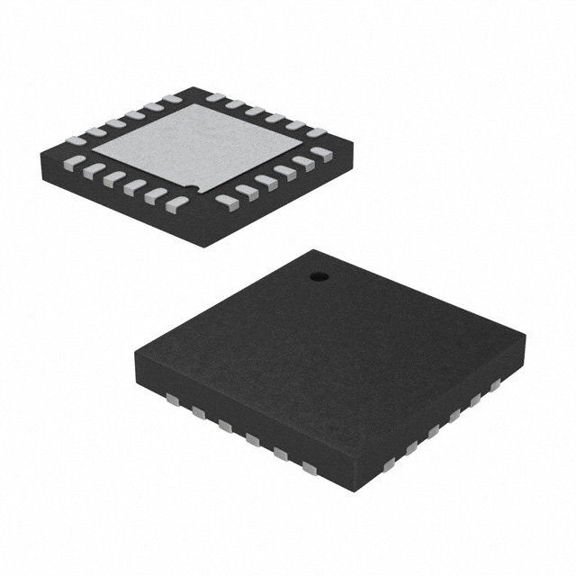
24-pin QFN (4 × 4 × 0.6 mm) Package
■
Application compatibility in standard and low-power systems
■
Commercial temperature range
Functional Description
For a complete list of related documentation, click here.
Logic Block Diagram
XIN/
EXCLKIN
XOUT
Crossbar
Switch
OSC
MUX
and
Control
Logic
FS0
FS1
Bank
1
PLL1
Output
Dividers
and
Drive
Strength
Control
PLL2
PLL3
(SS)
SCL
SDA
Serial
Interface
CLK1
CLK2
Bank
2
CLK3
CLK4
CLK5
Bank
3
CLK6
CLK7
CLK8
PLL4
(SS)
PD#/OE
Cypress Semiconductor Corporation
Document Number: 001-72951 Rev. *G
•
198 Champion Court
•
San Jose, CA 95134-1709
•
408-943-2600
Revised June 12, 2020
�CY2542
Contents
Pinouts .............................................................................. 3
Pin Definitions .................................................................. 4
Functional Overview ........................................................ 5
Four Configurable PLLs .............................................. 5
Two-wire Serial Interface Programming ...................... 5
Input Reference Clocks ............................................... 5
Output Power Supply Options ..................................... 5
Output Source Selection ............................................. 5
Spread Spectrum ........................................................ 5
Frequency Select ........................................................ 5
Glitch-Free Frequency Switch ..................................... 5
PD#/OE Mode ............................................................. 5
Keep Alive Mode ......................................................... 5
Output Drive Strength .................................................. 5
Factory Specific Configuration and
Custom Programming ................................................. 5
Two-wire Serial Interface ................................................. 6
Device Address ........................................................... 7
Data Valid .................................................................... 7
Data Frame ................................................................. 7
Acknowledge Pulse ..................................................... 7
Write Operations ............................................................... 8
Writing Individual Bytes ............................................... 8
Writing Multiple Bytes .................................................. 8
Read Operations ............................................................... 8
Current Address Read ................................................. 8
Random Read ............................................................. 8
Sequential Read .......................................................... 8
Document Number: 001-72951 Rev. *G
Serial I2C Programming Interface
Timing Specifications ...................................................... 8
Absolute Maximum Conditions ....................................... 9
Recommended Operating Conditions ............................ 9
DC Electrical Specifications .......................................... 10
AC Electrical Specifications .......................................... 11
Recommended Crystal Specification ........................... 12
Recommended Crystal Specification ........................... 12
Test and Measurement Setup ........................................ 12
Voltage and Timing Definitions ..................................... 13
Ordering Information ...................................................... 14
Ordering Code Definitions ......................................... 14
Package Diagrams .......................................................... 15
Acronyms ........................................................................ 16
Document Conventions ................................................. 16
Units of Measure ....................................................... 16
Document History Page ................................................. 17
Sales, Solutions, and Legal Information ...................... 18
Worldwide Sales and Design Support ....................... 18
Products .................................................................... 18
PSoC® Solutions ....................................................... 18
Cypress Developer Community ................................. 18
Technical Support ..................................................... 18
Page 2 of 18
�CY2542
Pinouts
21
20
GND
VDD
22
CLK8
23
DNU
24
XOUT
XIN/
EXCLKIN
Figure 1. 24-pin QFN pinout
19
1
18
GND
CLK1
2
17
CLK 7
VDD_ CLK_B1
3
16
VDD_ CLK_B3
PD#/OE
4
15
CLK 6
VDD
5
14
VDD_ CLK_B2
CLK2
6
13
CLK 5
CY2542
Document Number: 001-72951 Rev. *G
8
9
10
11
12
CLK3
CLK4
GND
GND
7
SDA/FS1
24 LD QFN
SCL /FSO
GND
Page 3 of 18
�CY2542
Pin Definitions
(VDD = 1.8 V Supply)
Pin Number
Name
I/O
Description
1
GND
Power
Power supply ground
2
CLK1
Output
Programmable clock output with spread spectrum. Output voltage depends on
VDD_CLK_B1 voltage
3
VDD_CLK_B1
Power
Power supply for Bank1 (CLK1, CLK2) outputs: 1.5 V/1.8 V/2.5 V/3.0 V/3.3 V
4
PD#/OE
Input
5
VDD
Power
Power supply: 1.8 V
6
CLK2
Output
Programmable clock output with spread spectrum. Output voltage depends on
VDD_CLK_B1 voltage
7
GND
Power
8
SCL/FS0
Input
9
SDA/FS1
10
CLK3
Output
Programmable clock output with no spread spectrum. Output voltage depends on
VDD_CLK_B2 voltage
11
CLK4
Output
Programmable clock output with no spread spectrum. Output voltage depends on
VDD_CLK_B2 voltage
12
GND
Power
Power supply ground
13
CLK5
Output
Programmable clock output with spread spectrum. Output voltage depends on
VDD_CLK_B2 voltage
Multifunction programmable pin: Output enable or power down modes
Power supply ground
Multifunction programmable pin: Serial data clock or Frequency select input pin
Input/Output Serial data input/output or Frequency select input pin
14
VDD_CLK_B2
Power
Power supply for Bank2 (CLK3, CLK4, CLK5) outputs: 1.5 V/1.8 V/2.5 V/3.0 V/3.3 V
15
CLK6
Output
Programmable clock output with spread spectrum. Output voltage depends on
VDD_CLK_B3 voltage
16
VDD_CLK_B3
Power
Power supply for Bank3 (CLK6, CLK7, CLK8) outputs: 1.5 V/1.8 V/2.5 V/3.0 V/3.3 V
17
CLK7
Output
Programmable clock output with spread spectrum. Output voltage depends on
VDD_CLK_B3 voltage
18
GND
Power
Power supply ground
19
GND
Power
Power supply ground
20
CLK8
Output
Programmable clock output with spread spectrum. Output voltage depends on
VDD_CLK_B3 voltage
21
DNU
None
Do not use
22
VDD
Power
Power supply: 1.8 V
23
XOUT
Output
Crystal output
24
XIN/EXCLKIN
Input
Document Number: 001-72951 Rev. *G
Crystal Input or 1.8 V external reference clock input
Page 4 of 18
�CY2542
Functional Overview
Four Configurable PLLs
The CY2542 is a four-PLL clock generator IC. It can be used to
generate four independent output frequencies ranging from 3 to
50 MHz (for 1.5 V/1.8 V output voltage) or 3-166 MHz (for
2.5 V/3.0 V/3.3 V output voltage) from a single crystal or a
reference clock.
Two-wire Serial Interface Programming
The CY2542 has a two-wire serial interface that programs the
configuration memory array to synthesize output frequencies by
programmable output divider, spread characteristics, and drive
strength. Two-wire Serial Interface can also be used for
in-system control of these programmable features.
Input Reference Clocks
The input to the CY2542 can be either a crystal or a clock signal.
The input frequency range for crystals is 8 MHz to 48 MHz, while
that for EXCLKIN is 1 to 48 MHz. The voltage level for the input
reference clock used must meet the voltage requirement for the
device as shown in the DC and AC specifications.
Output Power Supply Options
The CY2542 has eight clock outputs grouped in three banks. The
Bank 1, Bank 2, and Bank 3 correspond to (CLK1, CLK2), (CLK3,
CLK4, CLK5), and (CLK6, CLK7, CLK8) respectively. A separate
power supply is used for each of these three output drivers and
they can be any of 1.5 V, 1.8 V, 2.5 V, 3.0 V, or 3.3 V giving user
multiple choice of output clock voltage levels.
Output Source Selection
The CY2542 has eight clock outputs (CLK1–8). There are five
available clock sources for these outputs. These clock sources
are: XIN/EXCLKIN, PLL1, PLL2, PLL3 and PLL4. Output clock
source selection is done using four out of five crossbar switch.
Thus, any one of these five available clock sources can be
arbitrarily selected for the clock outputs. This gives user a
flexibility to have up to four independent clock and a reference
clock outputs.
Spread Spectrum
Two of the four PLLs (PLL3 and PLL4) have spread spectrum
capability for EMI reduction in the system. The device uses a
Cypress proprietary PLL and spread spectrum clock (SSC)
technology to synthesize and modulate the frequency of the PLL.
It can be factory programmed to either center spread range from
±0.125% to ±2.50%, or down spread range from –0.25% to –
5.0%, with Lexmark or Linear modulation profile.
Frequency Select
There are two multifunction frequency select pins (FS0, FS1)
that provide an option to select four different sets of frequencies
among each of the four PLLs. Each output has programmable
output divider options.
Document Number: 001-72951 Rev. *G
Glitch-Free Frequency Switch
When the frequency select pin (FS) is used to switch frequency,
the outputs are glitch-free provided frequency is switched using
output dividers. This feature enables uninterrupted system
operation while clock frequency is being switched.
PD#/OE Mode
PD#/OE input (Pin 4) can be programmed to operate as either
power down (PD#) or output enable (OE) mode. Note that power
down shuts off the entire chip, resulting in minimum power
consumption for the device. Setting this signal high brings the
device in the operational mode with default register settings. The
PD# turn-on time is limited by the turn-on time of the PLLs.
Disabled outputs are first driven to a low state before turning off.
When off, they are held low by internal weak resistors
(~160 k ohms)
When this pin is programmed as output enable (OE), clock
outputs can be enabled or disabled using OE (pin 4). Individual
clock outputs can be programmed to be sensitive to this OE pin.
Keep Alive Mode
By activating the device in the Keep Alive Mode, power down
mode is changed to power saving mode, which disables all PLLs
and outputs, but preserves the contents of the volatile registers.
Thus, any configuration changes made via two-wire serial
interface are preserved. By deactivating the Keep Alive Mode,
changes made due to serial interface is not preserved during
power down, but power consumption is reduced relative to the
Keep Alive Mode.
Output Drive Strength
The DC drive strength of the individual clock output can be
programmed for different values. Table 1 shows the typical rise
and fall times for different drive strength settings.
Table 1. Output Drive Strength
Output Drive Strength
Rise/Fall Time (ns)
(Typical Value)
Low
6.8
Mid Low
3.4
Mid High
2.0
High
1.0
Factory Specific Configuration and Custom
Programming
The device is available with factory specific programmed
frequencies as shown in the Ordering Information page. This
factory specific programmed part can be used for the device
evaluation purposes. The CY2542 can be custom programmed
to any desired frequencies and listed features. For customer
specific programming and two-wire Serial Interface programmable memory bitmap definitions, contact your local Cypress
Field Application Engineer (FAE) or sales representative.
Page 5 of 18
�CY2542
Two-wire Serial Interface
The two-wire serial interface uses two signals, SDA and SCL,
that operates up to 400 kbits/s in Read or Write mode. The SDA
and SCL timing and data transfer sequence is shown in Figure 2.
The basic Write serial format is as follows:
To enhance the flexibility and function of the clock synthesizer, a
two-signal serial interface is provided. This interface is used to
write (and optionally read) control registers that control various
device functions such as enabling individual clock output buffers.
The registers initialize to their default setting upon power up and
therefore, use of this interface is optional. Clock device registers
are normally changed upon system initialization. Any data written
via serial interface is volatile and is not retained when the device
is powered down.
Start Bit; 7-bit Device Address (DA); R/W Bit; Slave Clock
Acknowledge (ACK); 8-bit Memory Address (MA); ACK; 8-bit
Data; ACK; 8-bit Data in MA+1 if desired; ACK; 8-bit Data in
MA+2; ACK; etc. until STOP Bit. The basic serial format is
illustrated in Figure 3.
Figure 2. Data Transfer Sequence on the Serial Bus
SCL
SDA
Address or
Acknowledge
Valid
START
Condition
STOP
Condition
Data may
be changed
Figure 3. Data Frame Architecture
SDA Write
Multiple
Contiguous
Registers
1 Bit
1 Bit Slave
R/W = 0 ACK
7-bit
Device
Address
1 Bit
Slave
ACK
8-bit
Register
Address
(XXH)
1 Bit
Slave
ACK
8-bit
Register
Data
(XXH)
1 Bit
Slave
ACK
8-bit
Register
Data
(XXH+1)
8-bit
Register
Data
(XXH+2)
1 Bit
Slave
ACK
1 Bit
Slave
ACK
8-bit
Register
Data
(FFH)
1 Bit
Slave
ACK
8-bit
Register
Data
(00H)
Stop Signal
Start Signal
SDA Read
Current
Address
Read Start Signal
SDA Read
Multiple
Contiguous
Registers
1 Bit
Slave
ACK
1 Bit
1 Bit Slave
R/W = 1 ACK
7-bit
Device
Address
1 Bit
Slave
ACK
1 Bit
Master
NACK
8-bit
Register
Data
Stop Signal
1 Bit
1 Bit Slave
R/W = 0 ACK
7-bit
Device
Address
1 Bit
Slave
ACK
8-bit
Register
Address
(XXH)
1 Bit
Master
ACK
7-bit
Device
Address
+R/W=1
8-bit
Register
Data
(XXH)
1 Bit
Master
ACK
8-bit
Register
Data
(XXH+1)
1 Bit
Master
ACK
8-bit
Register
Data
(FFH)
1 Bit
Master
ACK
1 Bit
Master
ACK
1 Bit
Master
NACK
8-bit
Register
Data
(00H)
Stop Signal
Start Signal
Repeated
Start bit
Document Number: 001-72951 Rev. *G
Page 6 of 18
�CY2542
Device Address
Data Valid
The device serial interface address is 69H. The device address
is combined with a read/write bit as the LSB and is sent after
each start bit.
Data is valid when the clock is HIGH, and can only be
transitioned when the clock is LOW, as illustrated in Figure 4.
Figure 4. Data Valid and Data Transition Periods
SDAT
tf
tLOW
tr
tSU;DAT
tf
tHD;STA
tr
tBUF
SCLK
tHD;STA
tHD;DAT
S
tSU;STA
tHIGH
tSU;STO
Sr
P
S
Data Frame
Every new data frame is indicated by a start and stop sequence,
as illustrated in Figure 5.
Start Sequence – SDA going LOW when SCL is HIGH indicates
a Start Frame. Every time a start signal is supplied, the next 8-bit
data must be the device address (seven bits) and a R/W bit,
followed by register address (eight bits) and register data (eight
bits).
Stop Sequence – SDA going HIGH when SCL is HIGH indicates
a Stop Frame. A Stop Frame frees the bus to write to another part
on the same bus or to write to another random register address.
Figure 5. Start and Stop Frame
SDA
SCL
Transition
to next Bit
START
STOP
Acknowledge Pulse
During Write Mode, the CY2542 responds with an Acknowledge
pulse after every eight bits. This is done by pulling the SDA line
LOW during the N*9th clock cycle, as illustrated in Figure 6 (N =
the number of bytes transmitted). During Read Mode, the master
generates the acknowledge pulse after reading the data packet.
Figure 6. Frame Format (Device Address, R/W, Register Address, Register Data)
SDA
+
START
SCL
DA6
DA5 DA0
+
R/W
+
Document Number: 001-72951 Rev. *G
ACK
RA7
RA6 RA1
+
+
RA0
ACK
D7
D6
D1
D0
ACK
STOP
+
Page 7 of 18
�CY2542
Write Operations
Writing Individual Bytes
A valid write operation must have a full 8-bit register address
after the device address word from the master, which is followed
by an acknowledge bit from the slave (ACK = 0/LOW). The next
eight bits must contain the data word intended for storage. After
receiving the data word, the slave responds with another
acknowledge bit (ACK = 0/LOW), and the master must end the
write sequence with a STOP condition.
Writing Multiple Bytes
To write multiple bytes at a time, the master must not end the
write sequence with a STOP condition, but instead sends
multiple contiguous bytes of data to be stored. After each byte,
the slave responds with an acknowledge bit, the same as after
the first byte, and accepts data until the acknowledge bit is
responded to by the STOP condition. When receiving multiple
bytes, the CY2542 internally increments the register address.
operation returns the value stored in location ‘n+1’. When the
CY2542 receives the slave address with the R/W bit set to a ‘1’,
it issues an acknowledge and transmits the 8-bit word. The
master device does not acknowledge the transfer, but generates
a STOP condition, which causes CY2542 to stop transmission.
Random Read
Through random read operations, the master may access any
memory location. To perform this type of read operation, first set
the word address. To do this, send the address to the CY2542
as part of a write operation. After the word address is sent, the
master generates a START condition following the acknowledge.
This terminates the write operation before any data is stored in
the address, but not before the internal address pointer is set.
Next, the master reissues the control byte with the R/W byte set
to ‘1’. The CY2542 then issues an acknowledge and transmits
the 8-bit word. The master device does not acknowledge the
transfer, but generates a STOP condition, which causes the
CY2542 to stop transmission.
Sequential Read
Read Operations
Read operations are initiated the same way as Write operations
except that the R/W bit of the slave address is set to ‘1’ (HIGH).
There are three basic read operations: current address read,
random read, and sequential read.
Current Address Read
The CY2542 has an onboard address counter that retains ‘1’
more than the address of the last word accessed. If the last word
written or read was word ‘n’, then a current address read
Sequential read operations follow the same process as random
reads except that the master issues an acknowledge instead of
a STOP condition after transmission of the first 8-bit data word.
This action increments the internal address pointer, and
subsequently outputs the next 8-bit data word. By continuing to
issue acknowledges instead of STOP conditions, the master
serially reads the entire contents of the slave device memory.
When the internal address pointer points to the FFH register,
after the next increment, the pointer points to the 00H register.
Serial I2C Programming Interface Timing Specifications
Parameter
Description
Min
Max
Unit
–
400
kHz
Hold time START condition
0.6
–
μs
tLOW
Low period of the SCLK clock
1.3
–
μs
tHIGH
High period of the SCLK clock
0.6
–
μs
tSU:STA
Setup time for a repeated START condition
0.6
–
μs
tHD:DAT
Data hold time
100
–
ns
tSU:DAT
Data setup time
100
–
ns
tR
Rise time
–
300
ns
tF
Fall time
–
300
ns
tSU:STO
Setup time for STOP condition
0.6
–
μs
tBUF
Bus-free time between STOP and START conditions
1.3
–
μs
fSCLK
Frequency of SCLK
tHD:STA
Document Number: 001-72951 Rev. *G
Page 8 of 18
�CY2542
Absolute Maximum Conditions
Parameter
Description
VDD
Supply voltage
VDD_CLKX
Supply voltage
VIN
Input voltage
Condition
Min
Max
Unit
–0.5
2.8
V
–
–0.5
4.4
V
Relative to VSS
–0.5
2.2
V
–
TS
Temperature, storage
Non functional
–65
+150
°C
ESDHBM
ESD protection (human body
model)
JEDEC EIA/JESD22-A114-E
2000
–
V
UL-94
Flammability rating
V-0 @1/8 in.
–
10
ppm
MSL
Moisture sensitivity level
–
Unit
3
Recommended Operating Conditions
Parameter
Description
Min
Typ
Max
VDD
VDD operating voltage
1.65
1.80
1.95
V
VDD_CLK_BX
Output driver voltage
1.43
–
3.60
V
CLOAD
Maximum load capacitance
–
–
15
pF
tPU
Power up time for all VDDs to reach minimum specified voltage (power
ramps must be monotonic)
0.05
–
500
ms
TA
Ambient temperature, commercial
0
–
70
°C
Document Number: 001-72951 Rev. *G
Page 9 of 18
�CY2542
DC Electrical Specifications
(VDD_CLK_BX = 1.5 V/1.8 V/2.5 V/3.0 V/3.3 V)
Parameter
VOL
Description
Output low voltage, CLK pins
Conditions
IOL = 2 mA,
drive strength = [00]
Min
Typ
Max
Unit
–
–
0.4
V
VDD_CLK_BX – 0.4
–
–
V
–
–
0.4
V
IOL = 3 mA,
drive strength = [01]
IOL = 7 mA,
drive strength = [10]
IOL = 12 mA,
drive strength = [11]
VOH
Output high voltage, CLK pins
IOH = –2 mA,
drive strength = [00]
IOH = –3 mA,
drive strength = [01]
IOH = –7 mA,
drive strength = [10]
IOH = –12 mA,
drive strength = [11]
VOLSD
Output low voltage, SDA
IOL = 4 mA
VIL1
Input low voltage of PD#/OE,
SDA and SCL pins
–
–
0.2 × VDD
V
VIL2
Input low voltage of EXCLKIN pin
–
–
0.2 × VDD
V
VIH1
Input high voltage of PD#/OE,
SDA and SCL pins
0.8 × VDD
–
2.2
V
VIH2
Input high voltage of EXCLKIN
pin
0.8 × VDD
–
2.2
V
IIL1
Input low current, PD#/OE pin
VIL = 0 V
–
–
10
µA
IIH1
Input high current, PD#/OE pin
VIH = VDD
–
–
10
µA
RDN
Pull-down resistor of clocks
(CLK1-CLK8) in off-state
Clock outputs in off-state by
setting PD# = Low
100
160
250
kΩ
IDD[1, 2]
Supply current
All outputs running,
CLOAD = 0
–
15
–
mA
IDDS[1]
Standby current
PD# = Low, and serial
interface circuit not in Keep
Alive Mode
–
3
–
µA
CIN[2]
Input capacitance
SCL, SDA and PD#/OE
inputs
–
–
7
pF
Notes
1. This parameter is configuration dependent. The specified value is for the drive level setting of [1,1].
2. Parameters are guaranteed by design and characterization. Not 100% tested in production. All parameters specified with fully loaded outputs.
Document Number: 001-72951 Rev. *G
Page 10 of 18
�CY2542
AC Electrical Specifications
(VDD_CLK_BX = 1.5 V/1.8 V/2.5 V/3.0 V/3.3 V)
Min
Typ
Max
Unit
FCLK
Parameter
Clock output frequency
Description
All clock outputs
(for 1.5 V/1.8 V output voltage)
Conditions
3
–
50
MHz
FCLK
Clock output frequency
All clock outputs
(for 2.5 V/3.0 V/3.3 V output voltage)
3
–
166
MHz
FREF (crystal)
Crystal frequency, XIN
–
8
–
48
MHz
FREF (clock)
Input clock frequency, EXCLKIN –
1
–
48
MHz
DC
Output clock duty cycle
Duty Cycle is defined in Figure 8 on
page 13; t1/t2,
measured at 50% of VDD_CLK_BX
45
50
55
%
TRF1[4]
Output clock rise/fall time
Measured from 20% to 80% of
VDD_CLK_BX,
as shown in Figure 9 on page 13,
CLOAD = 15 pF,
drive strength [00]
–
6.8
10.0
ns
TRF2[4]
Output clock rise/fall time
Measured from 20% to 80% of
VDD_CLK_BX,
as shown in Figure 9 on page 13,
CLOAD = 15 pF,
drive strength [01]
–
3.4
5.0
ns
TRF3[4]
Output clock rise/fall time
Measured from 20% to 80% of
VDD_CLKX_BX,
as shown in Figure 9 on page 13,
CLOAD = 15 pF,
drive strength [10]
–
2.0
3.0
ns
TRF4[4]
Output clock rise/fall time
Measured from 20% to 80% of
VDD_CLKX_BX,
as shown in Figure 9 on page 13,
CLOAD = 15 pF,
drive strength [11]
–
1.0
1.5
ns
TCCJ[3, 4]
Cycle-to-cycle jitter
EXCLKIN = CLKx = 48 MHz,
CLOAD = 15 pF,
4 PLLs and 1 output for each PLL
enabled,
drive strength = [11]
–
150
–
ps
TLOCK[4]
PLL Lock time
–
–
1
3
ms
Notes
3. This parameter is configuration dependent. The specified value is for the drive level setting of [1,1].
4. Parameters are guaranteed by design and characterization. Not 100% tested in production. All parameters specified with fully loaded outputs.
Document Number: 001-72951 Rev. *G
Page 11 of 18
�CY2542
Recommended Crystal Specification
For SMD Package
Parameter
Description
MO
Mode of operation
Fmin
Minimum frequency
Range 1
Range 2
Range 3
Unit
28
MHz
Fundamental
8
14
Fmax
Maximum frequency
14
28
48
MHz
R1
Motional resistance (ESR)
135
50
30
Ω
C0
Shunt capacitance
4
4
2
pF
CL
Parallel load capacitance
18
14
12
pF
DL(max)
Maximum crystal drive level
300
300
300
µW
Range 2
Range 3
Unit
Recommended Crystal Specification
For Thru-Hole Package
Parameter
Description
Range 1
MO
Mode of operation
Fundamental
Fmin
Minimum frequency
8
14
24
MHz
Fmax
Maximum frequency
14
24
32
MHz
R1
Motional resistance (ESR)
90
50
30
Ω
C0
Shunt capacitance
7
7
7
pF
CL
Parallel load capacitance
DL(max)
Maximum crystal drive level
18
12
12
pF
1000
1000
1000
µW
Test and Measurement Setup
Figure 7. Test and Measurement Setup
VDD
Outputs
0.1 μF
DUT
CLOAD
GND
Document Number: 001-72951 Rev. *G
Page 12 of 18
�CY2542
Voltage and Timing Definitions
Figure 8. Duty Cycle Definition
t1
t2
V
DD_CLK_BX
50% of V
Clock
Output
DD_CLK_BX
0V
Figure 9. Rise Time = TRF, Fall Time = TRF
TRF
TRF
V
DD_CLKX_BX
80% of V
Clock
Output
Document Number: 001-72951 Rev. *G
DD_CLK_BX
20% of V
DD_CLKX_BX
0V
Page 13 of 18
�CY2542
Ordering Information
All product offerings are factory programmed customer specific devices with customized part numbers. Table 2 shows the available
device types, but not complete part numbers. Contact your local Cypress FAE or sales representative for more information.
Table 2. Possible Configurations
Part Number[5]
Type
VDD (V)
Production Flow
Pb-free
CY2542QCxxx
24-pin QFN
VDD = 1.8 V
VDD_CLK_Bx = 1.5/1.8/2.5/3.0/3.3 V
Commercial
CY2542QCxxxT
24-pin QFN - Tape and Reel
VDD = 1.8 V
VDD_CLK_Bx = 1.5/1.8/2.5/3.0/3.3 V
Commercial
Ordering Code Definitions
CY 2542
X
C
XXX
X
X = blank or T
blank = Tube; T = Tape and Reel
Three digit numeric custom configuration code
Temperature Range: C = Commercial
Package Type: X = Q
Q = 24-pin QFN (Pb-Free) 2.65 × 2.65 E-pad (Sawn type)
Base Part Number
Company ID: CY = Cypress
Note
5. xx indicates factory programmed parts based on customer specific configuration. For more details, contact your local Cypress FAE or sales representative.
Document Number: 001-72951 Rev. *G
Page 14 of 18
�CY2542
Package Diagrams
Figure 10. 24-pin QFN (4 × 4 × 0.55 mm) LQ24A (2.65 × 2.65 E-Pad (Sawn)) Package Outline, 001-13937
001-13937 *H
Document Number: 001-72951 Rev. *G
Page 15 of 18
�CY2542
Acronyms
Document Conventions
Table 3. Acronyms Used in this Document
Units of Measure
Acronym
Description
Table 4. Units of Measure
EMI
Electromagnetic Interference
FAE
Field Application Engineer
°C
degree Celsius
OE
Output Enable
kHz
kilohertz
PLL
Phase-Locked Loop
kΩ
kilo ohm
QFN
Quad Flat No-lead
MHz
megahertz
Spread Spectrum Clock
µA
microampere
µs
microsecond
µW
microwatt
SSC
Document Number: 001-72951 Rev. *G
Symbol
Unit of Measure
mA
milliampere
mm
millimeter
ms
millisecond
ns
nanosecond
Ω
ohm
ppm
parts per million
%
percent
pF
picofarad
ps
picosecond
V
volt
Page 16 of 18
�CY2542
Document History Page
Document Title: CY2542, Quad-PLL Programmable Spread Spectrum Clock Generator with Two-Wire Serial Interface and
Frequency Select
Document Number: 001-72951
Rev.
ECN No.
Submission
Date
Description of Change
**
3378470
11/14/2011
New data sheet.
*A
3507333
01/30/2012
Removed SSON pin related information in all instances across the document.
Replaced “I2C Serial Interface” with “two-wire Serial Interface” in all instances across the
document.
Updated Logic Block Diagram.
*B
4580483
12/11/2014
Updated Two-wire Serial Interface:
Updated Figure 3.
Updated Package Diagrams:
spec 51-85203 – Changed revision from *C to *D.
Updated to new template.
Completing Sunset Review.
*C
5258614
05/18/2016
Updated Two-wire Serial Interface:
Updated Data Valid:
Updated Figure 4.
Added Serial I2C Programming Interface Timing Specifications.
Removed “Two-wire Serial Programming Interface Timing Specifications”.
Updated Ordering Information:
Updated Table 2:
Updated part numbers.
Updated Package Diagrams:
Added spec 001-13937 *F (Figure 10).
Updated to new template.
*D
5381451
08/06/2016
Updated Features:
Replaced “24-pin (4 × 4 × 1 mm) QFN Package” with
“24-pin QFN (4 × 4 × 0.6 mm) Package”.
Updated Ordering Information:
Updated Table 2:
Updated part numbers.
Updated Package Diagrams:
Removed spec 51-85203 *D.
*E
5778002
06/19/2017
Updated Features:
Added one-time programmability.
Updated Functional Description:
Added “For a complete list of related documentation, click here.” at the end.
Updated Pin Definitions:
Updated details in “Description” column corresponding to pin numbers 2, 6, 10, 11, 13, 15,
17, and 20.
Updated to new template.
*F
5955206
11/02/2017
Updated Logic Block Diagram.
Updated DC Electrical Specifications:
Updated details in “Max” column corresponding to VIL2 parameter.
Updated details in “Max” column corresponding to VIH1 parameter.
Updated details in “Min” column corresponding to VIH2 parameter.
Updated to new template.
Completing Sunset Review.
*G
6897833
06/12/2020
Updated Package Diagrams:
spec 001-13937 – Changed revision from *F to *H.
Document Number: 001-72951 Rev. *G
Page 17 of 18
�CY2542
Sales, Solutions, and Legal Information
Worldwide Sales and Design Support
Cypress maintains a worldwide network of offices, solution centers, manufacturer’s representatives, and distributors. To find the office
closest to you, visit us at Cypress Locations.
PSoC® Solutions
Products
Arm® Cortex® Microcontrollers
Automotive
cypress.com/arm
cypress.com/automotive
Clocks & Buffers
Interface
cypress.com/clocks
cypress.com/interface
Internet of Things
Memory
cypress.com/iot
cypress.com/memory
Microcontrollers
cypress.com/mcu
PSoC
cypress.com/psoc
Power Management ICs
Cypress Developer Community
Community | Code Examples | Projects | Video | Blogs |
Training | Components
Technical Support
cypress.com/support
cypress.com/pmic
Touch Sensing
cypress.com/touch
USB Controllers
Wireless Connectivity
PSoC 1 | PSoC 3 | PSoC 4 | PSoC 5LP | PSoC 6 MCU
cypress.com/usb
cypress.com/wireless
© Cypress Semiconductor Corporation, 2011-2020. This document is the property of Cypress Semiconductor Corporation and its subsidiaries (“Cypress”). This document, including any software or
firmware included or referenced in this document (“Software”), is owned by Cypress under the intellectual property laws and treaties of the United States and other countries worldwide. Cypress reserves
all rights under such laws and treaties and does not, except as specifically stated in this paragraph, grant any license under its patents, copyrights, trademarks, or other intellectual property rights. If
the Software is not accompanied by a license agreement and you do not otherwise have a written agreement with Cypress governing the use of the Software, then Cypress hereby grants you a personal,
non-exclusive, nontransferable license (without the right to sublicense) (1) under its copyright rights in the Software (a) for Software provided in source code form, to modify and reproduce the Software
solely for use with Cypress hardware products, only internally within your organization, and (b) to distribute the Software in binary code form externally to end users (either directly or indirectly through
resellers and distributors), solely for use on Cypress hardware product units, and (2) under those claims of Cypress's patents that are infringed by the Software (as provided by Cypress, unmodified)
to make, use, distribute, and import the Software solely for use with Cypress hardware products. Any other use, reproduction, modification, translation, or compilation of the Software is prohibited.
TO THE EXTENT PERMITTED BY APPLICABLE LAW, CYPRESS MAKES NO WARRANTY OF ANY KIND, EXPRESS OR IMPLIED, WITH REGARD TO THIS DOCUMENT OR ANY SOFTWARE
OR ACCOMPANYING HARDWARE, INCLUDING, BUT NOT LIMITED TO, THE IMPLIED WARRANTIES OF MERCHANTABILITY AND FITNESS FOR A PARTICULAR PURPOSE. No computing
device can be absolutely secure. Therefore, despite security measures implemented in Cypress hardware or software products, Cypress shall have no liability arising out of any security breach, such
as unauthorized access to or use of a Cypress product. CYPRESS DOES NOT REPRESENT, WARRANT, OR GUARANTEE THAT CYPRESS PRODUCTS, OR SYSTEMS CREATED USING
CYPRESS PRODUCTS, WILL BE FREE FROM CORRUPTION, ATTACK, VIRUSES, INTERFERENCE, HACKING, DATA LOSS OR THEFT, OR OTHER SECURITY INTRUSION (collectively, “Security
Breach”). Cypress disclaims any liability relating to any Security Breach, and you shall and hereby do release Cypress from any claim, damage, or other liability arising from any Security Breach. In
addition, the products described in these materials may contain design defects or errors known as errata which may cause the product to deviate from published specifications. To the extent permitted
by applicable law, Cypress reserves the right to make changes to this document without further notice. Cypress does not assume any liability arising out of the application or use of any product or
circuit described in this document. Any information provided in this document, including any sample design information or programming code, is provided only for reference purposes. It is the responsibility
of the user of this document to properly design, program, and test the functionality and safety of any application made of this information and any resulting product. “High-Risk Device” means any
device or system whose failure could cause personal injury, death, or property damage. Examples of High-Risk Devices are weapons, nuclear installations, surgical implants, and other medical devices.
“Critical Component” means any component of a High-Risk Device whose failure to perform can be reasonably expected to cause, directly or indirectly, the failure of the High-Risk Device, or to affect
its safety or effectiveness. Cypress is not liable, in whole or in part, and you shall and hereby do release Cypress from any claim, damage, or other liability arising from any use of a Cypress product
as a Critical Component in a High-Risk Device. You shall indemnify and hold Cypress, its directors, officers, employees, agents, affiliates, distributors, and assigns harmless from and against all claims,
costs, damages, and expenses, arising out of any claim, including claims for product liability, personal injury or death, or property damage arising from any use of a Cypress product as a Critical
Component in a High-Risk Device. Cypress products are not intended or authorized for use as a Critical Component in any High-Risk Device except to the limited extent that (i) Cypress's published
data sheet for the product explicitly states Cypress has qualified the product for use in a specific High-Risk Device, or (ii) Cypress has given you advance written authorization to use the product as a
Critical Component in the specific High-Risk Device and you have signed a separate indemnification agreement.
Cypress, the Cypress logo, Spansion, the Spansion logo, and combinations thereof, WICED, PSoC, CapSense, EZ-USB, F-RAM, and Traveo are trademarks or registered trademarks of Cypress in
the United States and other countries. For a more complete list of Cypress trademarks, visit cypress.com. Other names and brands may be claimed as property of their respective owners.
Document Number: 001-72951 Rev. *G
Revised June 12, 2020
Page 18 of 18
�