CY28405-2
Clock Synthesizer with Differential SRC and CPU Outputs
Features
•
•
•
•
•
•
Supports Intel Pentium® 4-type CPUs
Selectable CPU frequencies
3.3V power supply
Nine copies of PCI clocks
Four copies of 3V66 with one optional VCH
Two copies 48-MHz clock
•
•
•
•
Three differential CPU clock pairs
One differential SRC clock
Support SMBus/I2 C Byte, Word and Block Read/ Write
Ideal Lexmark Spread Spectrum profile for maximum
electromagnetic interference (EMI) reduction
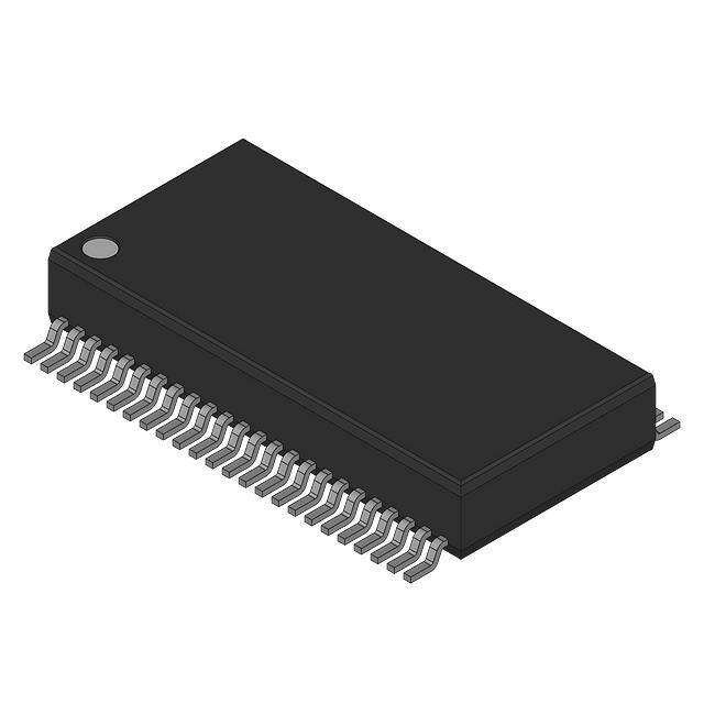
• 48-pin SSOP package
XTAL
OSC
FS_(A:B)
VTT_PWRGD#
PCI
REF
48M
x 4
x9
x2
x2
VDD_REF
REF(0:1)
PLL Ref Freq
VDD_CPU
CPUT(0:1, ITP), CPUC(0:1, ITP)
Divider
Network
VDD_SRCT
SRCT, SRCC
IREF
VDD_3V66
3V66_(0:2)
2
PCI(0:5)
3V66_3/VCH
VDD_48MHz
DOT_48
USB_48
PD#
I 2C
Logic
*FS_A/REF_0
*FS_B/REF_1
VDD_REF
XIN
XOUT
VSS_REF
PCIF0
PCIF1
PCIF2
VDD_PCI
VSS_PCI
PCI0
PCI1
PCI2
PCI3
VDD_PCI
VSS_PCI
PCI4
PCI5
PD#
DOT_48
USB_48
VSS_48
VDD_48
1
2
3
4
5
6
7
8
9
10
11
12
13
14
15
16
17
18
19
20
21
22
23
24
CY28405-2
VDD_PCI
PCIF(0:2)
PLL2
SDATA
SCLK
3V66
x1
Pin Configuration
~
PLL 1
SRC
x3
[1]
Block Diagram
XIN
XOUT
CPU
48
47
46
45
44
43
42
41
40
39
38
37
36
35
34
33
32
31
30
29
28
27
26
25
VDDA
VSSA
IREF
CPUT_ITP
CPUC_ITP
VSS_CPU
CPUT1
CPUC1
VDD_CPU
CPUT0
CPUC0
VSS_SRC
SRCT
SRCC
VDD_SRC
VTT_PWRGD#
SDATA*
SCLK*
3V66_0
3V66_1
VSS_3V66
VDD_3V66
3V66_2
3V66_3/VCH
SSOP-48
* 100k Internal Pull-up
Note:
1. Signals marked with [*] and [**] have internal pull-up and pull-down resistors, respectively.
CypressSemiconductorCorporation
Document #: 38-07511 Rev. *C
•
3901NorthFirstStreet
•
SanJose , CA 95134
•
408-943-2600
Revised Spetember 29, 2003
�CY28405-2
Pin Description
Pin No.
1
2
Name
FS_A/REF_0
FS_B/REF_1
Type
Description
I/O, SE
This pin is the FS_A at power-up and VTT_PWRGD# = 0, then it
becomes REF_0 output. (3.3V 14.318-MHz clock output.)
I/O, SE
This pin is the FS_B at power-up and VTT_PWRGD# = 0, then it
becomes REF_1 output. (3.3V 14.318-MHz clock output.)
I
Crystal Connection or External Reference Frequency Input. This
pin has dual functions. It can be used as an external 14.318-MHz
crystal connection or as an external reference frequency input.
4
XIN
5
XOUT
O, SE
Crystal Connection. Connection for an external 14.318-MHz crystal
output.
39, 42,
38, 41,
45, 44
CPUT(0:1),
CPUC(0:1),
CPUT_ITP,
CPUC_ITP
O, DIF
CPU Clock Output. Differential CPU clock outputs, see Table1 for
frequency configuration.l
36, 35
26, 29, 30
SRCT, SRCC
3V66(2:0)
O, DIF
O, SE
Differential Serial Reference Clock.
66-MHz Clock Output. 3.3V 66-MHz clock from internal VCO.
25
3V66_3/VCH
O, SE
48- or 66-MHz Clock Output. 3.3V selectable through SMBUS to be
66 MHz or 48 MHz. Default is 66-MHz.
7, 8, 9
PCI_F(0:2)
O, SE
Free Running PCI Output. 33-MHz clocks divided down from 3V66.
12, 13, 14, 15, 18, PCI(0:5)
19
O, SE
PCI Clock Output. 33MHz clocks divided down from 3V66.
22
21
USB_48
DOT_48
O, SE
O, SE
Fixed 48-MHz clock output.
Fixed 48-MHz clock output.
46
IREF
I
20
PD#
I, PU
33
VTT_PWRGD#
32
31
SDATA
SCLK
I/O, PU
I, PU
48
VDDA
PWR
3.3V power supply for PLL.
47
3, 10, 16, 24, 27,
34, 40
6, 11, 17, 23, 28,
37, 43
VSSA
VDD
GND
PWR
Ground for PLL.
3.3V Power supply for outputs.
VSS
GND
Ground for outputs.
I
Current Reference. A precision resistor is attached to this pin which
is connected to the internal current reference.
3.3V LVTTL input for PowerDown# active low.
3.3V LVTTL input is a level sensitive strobe used to latch the
FS[A:E] input (active low).
SMBus compatible SDATA.
SMBus compatible SCLOCK.
Frequency Select Pins (FS_A, FS_B)
Host clock frequency selection is achieved by applying the
appropriate logic levels to FS_A and FS_B inputs prior to
VTT_PWRGD# assertion (as seen by the clock synthesizer).
Upon VTT_PWRGD# being sampled low by the clock chip
(indicating processor VTT voltage is stable), the clock chip
samples the FS_A and FS_B input values. For all logic levels
of FS_A and FS_B VTT_PWRGD# employs a one-shot
functionality in that once a valid low on VTT_PWRGD# has
been sampled low, all further VTT_PWRGD#, FS_A, and
FS_B transitions will be ignored. Once “Test Clock Mode” has
been invoked, all further FS_B transitions will be ignored and
FS_A will asynchronously select between the Hi-Z and REF/N
mode. Exiting test mode is accomplished by cycling power
with FS_B in a high or low state.
Document #: 38-07511 Rev. *C
Page 2 of 16
�CY28405-2
Table 1. Frequency Select Table (FS_A FS_B)
FS_A
FS_B
CPU
SRC
3V66
PCIF/PCI
REF0
REF1
USB/DOT
0
0
100 MHz
100/200 MHz
66 MHz
33 MHz
14.3 MHz
14.31 MHz
48 MHz
0
0
B6b7
1
REF/N
200 MHz
REF/N
100/200 MHz
REF/N
66 MHz
REF/N
33 MHz
REF/N
14.3 MHz
REF/N
14.31 MHz
REF/N
48 MHz
1
0
133 MHz
100/200 MHz
66 MHz
33 MHz
14.3 MHz
14.31 MHz
48 MHz
1
B6b7
Hi-Z
Hi-Z
Hi-Z
Hi-Z
Hi-Z
Hi-Z
Hi-Z
Table 2. Frequency Select Table (FS_A FS_B) SMBus Bit 5 of Byte 6 = 1
FS_A
FS_B
CPU
SRC
3V66
PCIF/PCI
REF0
REF1
USB/DOT
0
0
200 MHz
100/200 MHz
66 MHz
33 MHz
14.3 MHz
14.31 MHz
48 MHz
0
1
1
0
400 MHz
266 MHz
100/200 MHz
100/200 MHz
66 MHz
66 MHz
33 MHz
33 MHz
14.3 MHz
14.3 MHz
14.31 MHz
14.31 MHz
48 MHz
48 MHz
Serial Data Interface
Data Protocol
To enhance the flexibility and function of the clock synthesizer,
a two-signal serial interface is provided. Through the Serial
Data Interface, various device functions, such as individual
clock output buffers, can be individually enabled or disabled.
The registers associated with the Serial Data Interface initializes to their default setting upon power-up, and therefore use
of this interface is optional. Clock device register changes are
normally made upon system initialization, if any are required.
The interface cannot be used during system operation for power management functions.
The clock driver serial protocol accepts byte write, byte read,
block write, and block read operations from the controller. For
block write/read operation, the bytes must be accessed in sequential order from lowest to highest byte (most significant bit
first) with the ability to stop after any complete byte has been
transferred. For byte write and byte read operations, the system controller can access individually indexed bytes. The offset of the indexed byte is encoded in the command code, as
described in Table3.
The block write and block read protocol is outlined in Table4
while Table5 outlines the corresponding byte write and byte
read protocol. The slave receiver address is 11010010 (D2h).
Table 3. Command Code Definition
Bit
7
(6:0)
Description
0 = Block read or block write operation, 1 = Byte read or byte write operation
Byte offset for byte read or byte write operation. For block read or block write operations, these bits should be
'0000000'
Table 4. Block Read and Block Write Protocol
Block Write Protocol
Bit
1
2:8
9
10
11:18
Description
Block Read Protocol
Start
Bit
1
Start
Slave address – 7 bits
2:8
Slave address – 7 bits
Write = 0
Acknowledge from slave
9
10
Write = 0
Acknowledge from slave
Command Code – 8 Bit
'00000000' stands for block operation
11:18
19
Acknowledge from slave
19
20:27
28
Byte Count – 8 bits
Acknowledge from slave
20
21:27
29:36
Data byte 1 – 8 bits
37
38:45
Acknowledge from slave
Data byte 2 – 8 bits
46
Acknowledge from slave
....
......................
Document #: 38-07511 Rev. *C
28
29
30:37
38
39:46
Description
Command Code – 8 Bit
'00000000' stands for block operation
Acknowledge from slave
Repeat start
Slave address – 7 bits
Read = 1
Acknowledge from slave
Byte count from slave – 8 bits
Acknowledge from master
Data byte from slave – 8 bits
Page 3 of 16
�CY28405-2
Table 4. Block Read and Block Write Protocol (continued)
Block Write Protocol
Description
Bit
Block Read Protocol
Description
Bit
....
Data Byte (N–1) –8 bits
47
....
....
Acknowledge from slave
Data Byte N –8 bits
48:55
56
Acknowledge from master
....
Acknowledge from slave
....
Data byte N from slave – 8 bits
....
Stop
....
....
Acknowledge from master
Stop
Data byte from slave – 8 bits
Acknowledge from master
Table 5. Byte Read and Byte Write Protocol
Byte Write Protocol
Bit
1
2:8
9
10
11:18
19
20:27
28
29
Byte Read Protocol
Description
Bit
Start
Slave address – 7 bits
1
2:8
Write = 0
9
Acknowledge from slave
Command Code – 8 bits
'100xxxxx' stands for byte operation, bits[6:0] of the
command code represents the offset of the byte to
be accessed
Acknowledge from slave
Data byte from master – 8 bits
Acknowledge from slave
Stop
10
11:18
19
20
21:27
28
29
30:37
Description
Start
Slave address – 7 bits
Write = 0
Acknowledge from slave
Command Code – 8 bits
'100xxxxx' stands for byte operation, bits[6:0] of
the command code represents the offset of the
byte to be accessed
Acknowledge from slave
Repeat start
Slave address – 7 bits
Read = 1
Acknowledge from slave
Data byte from slave – 8 bits
38
Acknowledge from master
39
Stop
Byte Configuration Map
Byte 0: Control Register
Bit
@Pup
7
0
Reserved
Name
Reserved, set = 0
6
1
PCIF
PCI
PCI Drive Strength Override
0 = Force All PCI and PCIF Outputs to Low Drive Strength
1 = Force All PCI and PCIF Outputs to High Drive Strength
5
0
Reserved
Reserved, set = 0
4
3
0
1
Reserved
Reserved
Reserved, set = 0
Reserved, set = 1
2
1
Reserved
Reserved, set = 1
1
0
HW
HW
FS_B
FS_A
Power-up latched value of FS_B pin
Power-up latched value of FS_A pin
Document #: 38-07511 Rev. *C
Description
Page 4 of 16
�CY28405-2
Byte 1: Control Register
Bit
7
@Pup
0
1
SRCT
SRCC
SRCT
SRCC
Reserved
6
1
5
Name
Description
Allow control of SRC during SW PCI_STP assertion
0 = Free Running, 1 = Stopped with SW PCI_STP
SRC Output Enable
0 = Disabled (three-state), 1 = Enabled
Reserved, set = 1
4
1
Reserved
Reserved, set = 1
3
2
1
1
Reserved
CPUT_ITP, CPUC_ITP
1
1
CPUT1, CPUC1
0
1
CPUT0, CPUC0
Reserved, set = 1
CPU_ITP Output Enable
0 = Disabled (three-state), 1 = Enabled
CPU(T/C)1 Output Enable,
0 = Disabled (three-state), 1 = Enabled
CPUT/C)0 Output Enable
0 = Disabled (three-state), 1 = Enabled
Byte 2: Control Register
Bit
@Pup
7
0
SRCT, SRCC
Name
SRCT/C Pwrdwn drive mode
0 = Driven in power-down, 1 = three-state in power-down
Description
6
0
SRCT, SRCC
SRC Stop drive mode
0 = Driven in PCI_STP, 1 = three-state in power-down
5
0
CPUT_ITP, CPUC_ITP
CPU(T/C)_ITP Pwrdwn drive mode
0 = Driven in power-down, 1 = three-state in power-down
4
0
CPUT1, CPUC1
CPU(T/C)1 Pwrdwn drive mode
0 = Driven in power-down, 1 = three-state in power-down
3
0
CPUT0, CPUC0
CPU(T/C)0 Pwrdwn drive mode
0 = Driven in power-down, 1 = three-state in power-down
2
0
Reserved
Reserved, set = 0
1
0
0
0
Reserved
Reserved
Reserved, set = 0
Reserved, set = 0
Byte 3: Control Register
Bit
@Pup
Name
7
1
SW PCI STOP
SW PCI_STP Function
0= PCI_STP assert, 1= PCI_STP deassert
When this bit is set to 0, all STOPPABLE PCI, PCIF and SRC outputs will
be stopped in a synchronous manner with no short pulses.
When this bit is set to 1, all STOPPED PCI,PCIF and SRC outputs will
resume in a synchronous manner with no short pulses.
6
1
Reserved
Reserved
5
1
PCI5
PCI5 Output Enable
0 = Disabled, 1 = Enabled
4
1
PCI4
PCI4 Output Enable
0 = Disabled, 1 = Enabled
3
1
PCI3
PCI3 Output Enable
0 = Disabled, 1 = Enabled
2
1
PCI2
PCI2 Output Enable
0 = Disabled, 1 = Enabled
1
1
PCI1
PCI1 Output Enable
0 = Disabled, 1 = Enabled
0
1
PCI0
PCI0 Output Enable
0 = Disabled, 1 = Enabled
Document #: 38-07511 Rev. *C
Description
Page 5 of 16
�CY28405-2
Byte 4: Control Register
Bit
7
@Pup
0
USB_48
Name
6
1
USB_48
5
0
PCIF2
4
0
PCIF1
3
0
PCIF0
2
1
PCIF2
1
1
PCIF1
0
1
PCIF0
Description
USB_48MHz Drive Strength Control
0 = Low Drive Strength, 1 = High Drive Strength
USB_48MHz Output Enable
0 = Disabled, 1 = Enabled
Allow control of PCIF2 with assertion of SW PCI_STP
0 = Free Running, 1 = Stopped with SW PCI_STP
Allow control of PCIF1 with assertion of SW PCI_STP
0 = Free Running, 1 = Stopped with SW PCI_STP
Allow control of PCIF0 with assertion of SW PCI_STP
0 = Free Running, 1 = Stopped with SW PCI_STP
PCIF2 Output Enable
0 = Disabled, 1 = Enabled
PCIF1 Output Enable
0 = Disabled, 1 = Enabled
PCIF0 Output Enable
0 = Disabled, 1 = Enabled
Byte 5: Control Register
Bit
@Pup
Name
Description
7
1
DOT_48
DOT_48MHz Output Enable
0 = Disabled, 1 = Enabled
6
1
Reserved
Reserved, set = 1
5
0
3V66_3/VCH
4
1
3V66_3/VCH
3
1
Reserved
3V66_3/VCH Frequency Select
0 = 3V66 mode, 1 = VCH (48MHz) mode
3V66_3/VCH Output Enable
0 = Disabled, 1 = Enabled
Reserved, set = 1
2
1
3V66_2
3V66_2 Output Enable
0 = Disabled, 1 = Enabled
1
1
3V66_1
3V66_1 Output Enable
0 = Disabled, 1 = Enabled
0
1
3V66_0
3V66_0 Output Enable
0 = Disabled, 1 = Enabled
Byte 6: Control Register
Bit
@Pup
7
6
0
0
Reserved
Reserved
Name
Reserved, set = 0
Reserved, set = 0
5
0
FS_A & FS_B Operation
0 = Normal, 1 = Test mode
4
0
CPUC0, CPUT0
CPUC1, CPUT1
CPUT_ITP,CPUC_ITP
SRCT, SRCC
3
0
PCIF
PCI
3V66
SRCT,SRCC
CPUT_ITP,CPUC_ITP
Document #: 38-07511 Rev. *C
Description
SRCT/C Frequency Select
0 = 100Mhz, 1 = 200MHz
Spread Spectrum Mode
0 = down (default), 1 = center
Page 6 of 16
�CY28405-2
Byte 6: Control Register (continued)
Bit
2
@Pup
0
1
1
Name
PCIF
PCI
3V66
SRCT,SRCC
CPUT_ITP,CPUC_ITP
REF_1
0
1
REF_0
Description
Spread Spectrum Enable
0 = Spread Off, 1 = Spread On
REF_1 Output Enable
0 = Disabled, 1 = Enabled
REF_0 Output Enable
0 = Disabled, 1 = Enabled
Byte 7: Control Register
Bit
7
6
5
4
3
2
1
0
@Pup
0
1
0
0
1
0
0
0
Name
Revision ID Bit 3
Revision ID Bit 2
Revision ID Bit 1
Revision ID Bit 0
Vendor ID Bit 3
Vendor ID Bit 2
Vendor ID Bit 1
Vendor ID Bit 0
Description
Revision ID Bit 3
Revision ID Bit 2
Revision ID Bit 1
Revision ID Bit 0
Vendor ID Bit 3
Vendor ID Bit 2
Vendor ID Bit 1
Vendor ID Bit 0
Crystal Recommendations
The CY28405-2 requires a Parallel Resonance Crystal.
Substituting a series resonance crystal will cause the
CY28405-2 to operate at the wrong frequency and violate the
ppm specification. For most applications there is a 300-ppm
frequency shift between series and parallel crystals due to
incorrect loading.
Table 6. Crystal Recommendations
Frequency
(Fund)
14.31818 MHz
Cut
AT
Loading Load Cap
Parallel
20 pF
Drive
(max.)
0.1 mW
Shunt Cap
(max.)
5 pF
Motional
(max.)
0.016 pF
Tolerance
(max.)
50 ppm
Stability
(max.)
50 ppm
Aging
(max.)
5 ppm
Crystal Loading
Crystal loading plays a critical role in achieving low ppm performance. To realize low ppm performance, the total capacitance
the crystal will see must be considered to calculate the appropriate capacitive loading (CL).
The following diagram shows a typical crystal configuration
using the two trim capacitors. An important clarification for the
following discussion is that the trim capacitors are in series
with the crystal not parallel. It’s a common misconception that
load capacitors are in parallel with the crystal and should be
approximately equal to the load capacitance of the crystal.
This is not true.
Document #: 38-07511 Rev. *C
Figure 1.Crystal Capacitive Clarification
Page 7 of 16
�CY28405-2
As mentioned previously, the capacitance on each side of the
crystal is in series with the crystal. This mean the total capacitance on each side of the crystal must be twice the specified
load capacitance (CL). While the capacitance on each side of
the crystal is in series with the crystal, trim capacitors(Ce1,Ce2) should be calculated to provide equal capacitative loading on both sides.
Calculating Load Capacitors
In addition to the standard external trim capacitors, trace
capacitance and pin capacitance must also be considered to
correctly calculate crystal loading. As mentioned previously,
the capacitance on each side of the crystal is in series with the
crystal. This means the total capacitance on each side of the
crystal must be twice the specified crystal load capacitance
(CL). While the capacitance on each side of the crystal is in
series with the crystal, trim capacitors (Ce1,Ce2) should be
calculated to provide equal capacitive loading on both sides.
Use the following formulas to calculate the trim capacitor
values fro Ce1 and Ce2.
Clock Chip
(CY28405-2)
Ci2
Ci1
Pin
3 to 6p
Cs1
X2
X1
Cs2
Trace
2.8pF
XTAL
Ce1
Ce2
Trim
33pF
Figure 2.Crystal Loading Example
Load Capacitance (each side)
Ce = 2 * CL – (Cs + Ci)
CL ...................................................Crystal load capacitance
CLe ........................................ Actual loading seen by crystal
..................................... using standard value trim capacitors
Ce .................................................... External trim capacitors
Cs............................................. Stray capacitance (trace,etc)
Ci ............. Internal capacitance (lead frame, bond wires etc)
PD# (Power-down) Clarification
The PD# (Power Down) pin is used to shut off ALL clocks prior
to shutting off power to the device. PD# is an asynchronous
active LOW input. This signal is synchronized internally to the
device powering down the clock synthesizer. PD# is an
asynchronous function for powering up the system. When PD#
Document #: 38-07511 Rev. *C
Total Capacitance (as seen by the crystal)
CLe
=
1
1
( Ce1 + Cs1
+ Ci1 +
1
Ce2 + Cs2 + Ci2
)
is low, all clocks are driven to a LOW value and held there and
the VCO and PLLs are also powered down. All clocks are shut
down in a synchronous manner so has not to cause glitches
while transitioning to the low ‘stopped’ state.
PD# – Assertion
When PD# is sampled low by two consecutive rising edges of
CPUC clock then all clock outputs (except CPU) clocks must
be held low on their next high to low transition. CPU clocks
must be hold with CPU clock pin driven high with a value of 2x
Iref and CPUC undriven.
Due to the state of internal logic, stopping and holding the REF
clock outputs in the LOW state may require more than one
clock cycle to complete.
Page 8 of 16
�CY28405-2
PD#
CPUT, 133MHz
CPUC, 133MHz
SRCT 100MHz
SRCC 100MHz
3V66, 66MHz
USB, 48MHz
PCI, 33MHz
REF
Figure 3.Power-down Assertion Timing Waveforms
PD# Deassertion
The power-up latency between PD# rising to a valid logic ‘1’
level and the starting of all clocks is less than 3.0 ms.
Tstable
0.25mS
VTT_PWRGD# = Low
Sample
Inputs straps
VDD_A = 2.0V
Wait for


 工商网监
湘ICP备2023018690号
工商网监
湘ICP备2023018690号