CY29773
2.5V or 3.3V, 200-MHz, 12-Output Zero
Delay Buffer
Features
Description
• 6 ps typical period jitter
The CY29773 is a low-voltage high-performance 200-MHz
PLL-based zero delay buffer designed for high-speed clock
distribution applications.
• Output frequency range: 8.33 MHz to 200 MHz
• Input frequency range: 6.25 MHz to 125 MHz
• 2.5V or 3.3V operation
• Split 2.5V/3.3V outputs
• 12 Clock outputs: drive up to 24 clock lines
• One feedback output
• Three reference clock inputs: LVPECL or LVCMOS
• Phase-locked loop (PLL) bypass mode
• Spread Aware™
The CY29773 features one LVPECL and two LVCMOS
reference clock inputs and provides 12 outputs partitioned in
three banks of four outputs each. Each bank divides the VCO
output per SEL(A:C) settings (see Table 2. Function Table
(Configuration Controls)). These dividers allow output-to-input
ratios of 8:1, 6:1, 5:1, 4:1, 3:1, 8:3, 5:2, 2:1, 5:3, 3:2, 4:3, 5:4,
1:1, and 5:6. Each LVCMOS-compatible output can drive 50Ω
series- or parallel-terminated transmission lines. For
series-terminated transmission lines, each output can drive
one or two traces, giving the device an effective fanout of 1:24.
The PLL is ensured stable, given that the VCO is configured
to run between 200 MHz to 500 MHz. This allows a wide range
of output frequencies, from 8 MHz to 200 MHz. For normal
operation, the external feedback input FB_IN is connected to
the feedback output FB_OUT. The internal VCO is running at
multiples of the input reference clock set by the feedback
divider (see Table 1. Frequency Table).
• Output enable/disable
• Pin-compatible with MPC9773 and MPC973
• Industrial temperature range: –40°C to +85°C
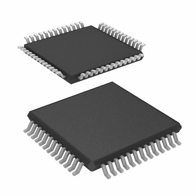
• 52-pin 1.0-mm TQFP package
When PLL_EN is LOW, PLL is bypassed and the reference
clock directly feeds the output dividers. This mode is fully static
and the minimum input clock frequency specification does not
apply.
Pin Configuration
Block Diagram
QB3
MR#/OE
D Q
Sync
Frz
D Q
Sync
Frz
/4, /6, /8, /12
/2, /4, /6, /8
QC2
1
2
3
4
5
6
7
8
9
10
11
12
13
39
38
37
36
35
34
33
32
31
30
29
28
27
C Y29773
V SS
QB0
V DDQB
QB1
V SS
QB2
V DDQB
QB3
FB_IN
V SS
FB_OUT
V DD
FB_SEL0
14 15 16 17 18 19 20 21 22 23 24 25 26
QC3
FB_SEL1
SYNC
VSS
SYNC
QC0
Sync
Frz
VDDQC
D Q
QC1
Data Generator
SELC0
FB_OUT
SELC1
Sync
Frz
QC2
D Q
VDDQC
0
1
QC3
/2
VSS
/4, /6, /8, /10
INV_CLK
2
QC0
QC1
/4, /6, /8, /10
Sync Pulse
FB_SEL(0,1)
SELB1
QB0
QB2
2
SELB0
A V SS
MR#/OE
SCLK
SDA TA
FB_SEL2
PLL_EN
REF_SEL
TCLK_SEL
TCLK0
TCLK1
PECL_CLK
PECL_CLK#
A V DD
QB1
SELC(0,1)
SELA1
Sync
Frz
FB_SEL2
SELB(0,1)
SELA0
D Q
2
QA3
FB_IN
2
VDDQA
52 51 50 49 48 47 46 45 44 43 42 41 40
QA2
QA3
SELA(0,1)
QA2
QA1
LPF
Power-On
Reset
VSS
QA0
QA1
Sync
Frz
VDDQA
0
1
VCO
QA0
TCLK1
TCLK_SEL
Phase
Detector
0
1
VSS
D Q
TCLK0
VCO_SEL
PECL_CLK
PECL_CLK#
VCO_SEL
PLL_EN
REF_SEL
SCLK
SDATA
Output Disable
Circuitry
12
INV_CLK
Cypress Semiconductor Corporation
Document #: 38-07573 Rev. *A
•
198 Champion Court
•
San Jose, CA 95134-1709
•
408-943-2600
Revised October 27, 2005
�CY29773
Pin Description [1]
Pin
Name
I/O
Type
Description
11
PECL_CLK
I, PU
LVPECL
LVPECL reference clock input.
12
PECL_CLK#
I
LVPECL
LVPECL reference clock input.
9
TCLK0
I, PU
LVCMOS LVCMOS/LVTTL reference clock input.
10
TCLK1
I, PU
LVCMOS LVCMOS/LVTTL reference clock input.
44,46,48,50
QA(3:0)
O
LVCMOS Clock output bank A.
32,34,36,38
QB(3:0)
O
LVCMOS Clock output bank B.
16,18,21,23
QC(3:0)
O
LVCMOS Clock output bank C.
29
FB_OUT
O
LVCMOS Feedback clock output. Connect to FB_IN for normal operation.
31
FB_IN
I, PU
LVCMOS Feedback clock input. Connect to FB_OUT for normal operation. This
input should be at the same voltage rail as input reference clock. See
Table 1. Frequency Table.
25
SYNC
O
LVCMOS Synchronous pulse output. This output is used for system synchronization.
6
PLL_EN
I, PU
LVCMOS PLL enable/bypass input. When Low, PLL is disabled/bypassed and
the input clock connects to the output dividers.
2
MR#/OE
I, PU
LVCMOS Master reset and Output enable/disable input. See Table 2.
Function Table (Configuration Controls).
8
TCLK_SEL
I, PU
LVCMOS LVCMOS Clock reference select input. See Table 2. Function Table
(Configuration Controls).
7
REF_SEL
I, PU
LVCMOS LVCMOS/LVPECL Reference select input. See Table 2. Function
Table (Configuration Controls).
52
VCO_SEL
I, PU
LVCMOS VCO Operating frequency select input. See Table 2. Function Table
(Configuration Controls).
14
INV_CLK
I, PU
LVCMOS QC(2,3) Phase selection input. See Table 2. Function Table (Configuration Controls).
5,26,27
FB_SEL(2:0) I, PU
LVCMOS Feedback divider select input. See Table 6.
42,43
SELA(1,0)
I, PU
LVCMOS Frequency select input, Bank A. See Table 3. Function Table (Bank
A).
40,41
SELB(1,0)
I, PU
LVCMOS Frequency select input, Bank B. See Table 4. Function Table (Bank
B).
19,20
SELC(1,0)
I, PU
LVCMOS Frequency select input, Bank C. See Table 5. Function Table (Bank
C).
3
SCLK
I, PU
LVCMOS Serial clock input.
4
SDATA
I, PU
LVCMOS Serial data input.
45,49
VDDQA
Supply
VDD
2.5V or 3.3V Power supply for bank A output clocks.[2,3]
33,37
VDDQB
Supply
VDD
2.5V or 3.3V Power supply for bank B output clocks.[2,3]
22,17
VDDQC
Supply
VDD
2.5V or 3.3V Power supply for bank C output clocks.[2,3]
13
AVDD
Supply
VDD
2.5V or 3.3V Power supply for PLL.[2,3]
28
VDD
Supply
VDD
2.5V or 3.3V Power supply for core and inputs.[2,3]
1
AVSS
Supply
Ground
Analog Ground.
Supply
Ground
Common Ground.
15,24,30,35,39,47,51 VSS
Notes:
1. PU = Internal pull-up, PD = Internal pull-down.
2. A 0.1-µF bypass capacitor should be placed as close as possible to each positive power pin ( 100 MHz
45
–
55
tr, tf
Output Rise/Fall times
0.6V to 1.8V
0.1
–
1.0
ns
t(φ)
Propagation Delay (static phase
offset)
TCLK to FB_IN
–125
–
125
ps
PCLK to FB_IN
–125
–
125
Notes:
7. AC characteristics apply for parallel output termination of 50Ω to VTT. Outputs are at same supply voltage unless otherwise stated. Parameters are guaranteed
by characterization and are not 100% tested.
8. VCMR (AC) is the crosspoint of the differential input signal. Normal AC operation is obtained when the crosspoint is within the VCMR range and the input swing
lies within the VPP (AC) specification. Violation of VCMR or VPP impacts static phase offset t(φ).
Document #: 38-07573 Rev. *A
Page 6 of 13
�CY29773
AC Electrical Specifications (VDD = 2.5V ±5%, TA = –40°C to +85°C)[7]
Parameter
tsk(O)
Description
Condition
Output-to-Output Skew
Skew within Bank A
Min.
Typ.
Max.
Unit
–
–
75
ps
Skew within Bank B
–
–
100
Skew within Bank C
–
–
150
tsk(B)
Bank-to-Bank Skew
–
–
400
ps
tPLZ, HZ
Output Disable Time
–
–
10
ns
tPZL, ZH
Output Enable Time
–
–
10
ns
BW
PLL Closed Loop Bandwidth (-3dB) ÷4 Feedback
–
1.3–2.0
–
MHz
÷6 Feedback
–
0.7–1.3
–
÷8 Feedback
–
0.9–1.3
–
÷10 Feedback
–
0.6–1.1
–
÷12 Feedback
–
0.6–0.9
–
÷16 Feedback
–
0.4–0.6
–
÷20 Feedback
–
0.6–0.9
–
Same frequency (125 MHz)
RMS (1σ)
–
7
30
tJIT(CC)
tJIT(PER)
Cycle-to-Cycle Jitter
Period Jitter
Same frequency
–
–
150
Multiple frequencies
–
–
435
Same frequency (125 MHz)
RMS (1σ)
–
6
30
Same frequency
–
45
75
Multiple frequencies
–
–
235
ps
ps
tJIT(φ)
I/O Phase Jitter
–
–
150
ps
tLOCK
Maximum PLL Lock Time
–
–
1
ms
Min.
Typ.
Max.
Unit
200
–
500
MHz
÷4 Feedback
50
–
125
MHz
÷6 Feedback
33.3
–
83.3
AC Electrical Specifications (VDD = 3.3V ±5%, TA = –40°C to +85°C)[7]
Parameter
Description
fVCO
VCO Frequency
fin
Input Frequency
Condition
÷8 Feedback
25
–
62.5
÷10 Feedback
20
–
50
÷12 Feedback
16.6
–
41.6
÷16 Feedback
12.5
–
31.25
÷20 Feedback
10
–
25
÷24 Feedback
8.3
–
20.8
÷32 Feedback
6.25
–
15.625
÷40 Feedback
5
–
12.5
0
–
200
25
–
75
%
Bypass mode (PLL_EN = 0)
frefDC
Input Duty Cycle
VPP
Peak-Peak Input Voltage
LVPECL
500
–
1000
mV
VCMR
Common Mode Range[8]
LVPECL
1.2
–
VDD–0.9
V
tr, tf
TCLK Input Rise/FallTime
0.8V to 2.0V
–
–
1.0
ns
Document #: 38-07573 Rev. *A
Page 7 of 13
�CY29773
AC Electrical Specifications (VDD = 3.3V ±5%, TA = –40°C to +85°C)[7]
Parameter
fMAX
fMAX
Description
Maximum Output Frequency
Maximum Output Frequency
(continued)
Condition
Min.
Typ.
Max.
Unit
100
–
200
MHz
÷4 Output
50
–
125
÷6 Output
33.3
–
83.3
÷2 Output
÷8 Output
25
–
62.5
÷10 Output
20
–
50
MHz
÷12 Output
16.6
–
41.6
÷16 Output
12.5
–
31.25
÷20 Output
10
–
25
÷24 Output
8.3
–
20.8
–
–
20
MHz
48
–
52
%
fSCLK
Serial Clock Frequency
DC
Output Duty Cycle
fMAX < 100 MHz
fMAX > 100 MHz
45
–
55
tr, tf
Output Rise/Fall times
0.55V to 2.4V
0.1
–
1.0
ns
t(φ)
Propagation Delay (static phase
offset)
TCLK to FB_IN, same VDD
–125
–
125
ps
PCLK to FB_IN, same VDD
–125
–
125
tsk(O)
Output-to-Output Skew
Skew within Bank A
–
–
75
Skew within Bank B
–
–
100
Skew within Bank C
ps
–
–
150
tsk(B)
Bank-to-Bank Skew
–
–
325
ps
tPLZ, HZ
Output Disable Time
–
–
8
ns
tPZL, ZH
Output Enable Time
–
–
8
ns
BW
PLL Closed Loop Bandwidth
(–3 dB)
÷4 Feedback
–
1.3–2.0
–
MHz
÷6 Feedback
–
0.7–1.3
–
tJIT(CC)
tJIT(PER)
Cycle-to-Cycle Jitter
Period Jitter
tJIT(φ)
I/O Phase Jitter
tLOCK
Maximum PLL Lock Time
÷8 Feedback
–
0.9–1.3
–
÷10 Feedback
–
0.6–1.1
–
÷12 Feedback
–
0.6–0.9
–
÷16 Feedback
–
0.4–0.6
–
÷20 Feedback
–
0.6–0.9
–
Same frequency (125 MHz)
RMS (1σ)
–
7
30
Same frequency
–
–
100
Multiple frequencies
–
–
375
Same frequency (125 MHz)
RMS (1σ)
–
6
30
Same frequency
––
45
75
Multiple frequencies
–
–
225
I/O same VDD
–
–
150
ps
–
–
1
ms
SYNC Output
In situations where output frequency relationships are not
integer multiples of each other the SYNC output provides a
signal for system synchronization. The CY29773 monitors the
relationship between the QA and the QC output clocks. It
provides a low going pulse, one period in duration, one period
prior to the coincident rising edges of the QA and QC outputs.
Document #: 38-07573 Rev. *A
ps
ps
The duration and the placement of the pulse depend on the
higher of the QA and QC output frequencies. Figure 1 illustrates various waveforms for the SYNC output. Note that the
SYNC output is defined for all possible combinations of the QA
and QC outputs even though under some relationships the
lower frequency clock could be used as a synchronizing
signal.
Page 8 of 13
�CY29773
VCO
1:1 Mode
QA
QC
SYNC
2:1 Mode
QA
QC
SYNC
3:1 Mode
QC
QA
SYNC
3:2 Mode
QA
QC
SYNC
4:1 Mode
QC
QA
SYNC
4:3 Mode
QA
QC
SYNC
6:1 Mode
QA
QC
SYNC
Figure 1.
Power Management
The individual output enable/freeze control of the CY29773
allows the user to implement unique power management
schemes into the design. The outputs are stopped in the logic
‘0’ state when the freeze control bits are activated. The serial
input register contains one programmable freeze enable bit for
12 of the 14 output clocks. The QC0 and FB_OUT outputs can
not be frozen with the serial port, this avoids any potential lock
up situation should an error occur in the loading of the serial
Document #: 38-07573 Rev. *A
data. An output is frozen when a logic ‘0’ is programmed and
enabled when a logic ‘1’ is written. The enabling and freezing
of individual outputs is done in such a manner as to eliminate
the possibility of partial “runt” clocks.
The serial input register is programmed through the SDATA
input by writing a logic ‘0’ start bit followed by 12 NRZ freeze
enable bits. The period of each SDATA bit equals the period of
the free running SCLK signal. The SDATA is sampled on the
rising edge of SCLK.
Page 9 of 13
�CY29773
Start
Bit
D0 D1 D2 D3 D4 D5 D6 D7 D8 D9 D10 D11
D0-D3 are the control bits for QA0-QA3, respectively
D4-D7 are the control bits for QB0-QB3, respectively
D8-D10 are the control bits for QC1-QC3, respectively
D11 is the control bit for SYNC
Figure 2.
Zo = 50 ohm
Pulse
Generator
Z = 50 ohm
Zo = 50 ohm
R T = 50 ohm
R T = 50 ohm
VTT
VTT
Figure 3. LVCMOS_CLK AC Test Reference for VDD = 3.3V/2.5V
Zo = 50 ohm
Differential
Pulse
Generator
Z = 50 ohm
Zo = 50 ohm
Zo = 50 ohm
R T = 50 ohm
VTT
R T = 50 ohm
VTT
Figure 4. PECL_CLK AC Test Reference for VDD = 3.3V/2.5V
PECL_CLK
VPP
PECL_CLK
VCMR
VDD
FB_IN
VDD/2
t(φ)
GND
Figure 5. LVPECL Propagation Delay t(φ), Static Phase Offset
VDD
LVCMOS_CLK
VDD/2
GND
VDD
FB_IN
VDD/2
t(φ)
GND
Figure 6. LVCMOS Propagation Delay t(φ), Static Phase Offset
Document #: 38-07573 Rev. *A
Page 10 of 13
�CY29773
VDD
VDD/2
tP
GND
T0
DC = tP / T0 x 100%
Figure 7. Output Duty Cycle (DC)
VDD
VDD/2
GND
VDD
VDD/2
tSK(O)
GND
Figure 8. Output-to-Output Skew, tsk(O)
Ordering Information
Part Number
Package Type
Product Flow
CY29773AI
52-pin TQFP
Industrial, –40°C to +85°C
CY29773AIT
52-pin TQFP – Tape and Reel
Industrial, –40°C to 85°C
CY29773AXI
52-pin TQFP
Industrial, –40°C to +85°C
CY29773AXIT
52-pin TQFP – Tape and Reel
Industrial, –40°C to 85°C
Lead-free
Document #: 38-07573 Rev. *A
Page 11 of 13
�CY29773
Package Drawing and Dimension
52-Lead Thin Plastic Quad Flat Pack (10 x 10 x 1.0 mm) A52B
51-85158-**
Spread Aware is a trademark of Cypress Semiconductor. All product and company names mentioned in this document are the
trademarks of their respective holders.
Document #: 38-07573 Rev. *A
Page 12 of 13
© Cypress Semiconductor Corporation, 2005. The information contained herein is subject to change without notice. Cypress Semiconductor Corporation assumes no responsibility for the use
of any circuitry other than circuitry embodied in a Cypress product. Nor does it convey or imply any license under patent or other rights. Cypress products are not warranted nor intended to be
used for medical, life support, life saving, critical control or safety applications, unless pursuant to an express written agreement with Cypress. Furthermore, Cypress does not authorize its
products for use as critical components in life-support systems where a malfunction or failure may reasonably be expected to result in significant injury to the user. The inclusion of Cypress
products in life-support systems application implies that the manufacturer assumes all risk of such use and in doing so indemnifies Cypress against all charges.
�CY29773
Document History Page
Document Title:CY29773 2.5V or 3.3V, 200-MHz, 12-Output Zero Delay Buffer
Document Number: 38-07573
REV.
ECN No.
Issue Date
Orig. of
Change
Description of Change
**
129007
09/02/03
RGL
New Data Sheet
*A
404290
See ECN
RGL
Added pb-free devices
added typical data for period jitter
Document #: 38-07573 Rev. *A
Page 13 of 13
�


 工商网监
湘ICP备2023018690号
工商网监
湘ICP备2023018690号
