CY29940
2.5 V or 3.3 V, 200-MHz, 1:18 Clock Distribution Buffer
2.5 V or 3.3 V, 200-MHz, 1:18 Clock Distribution Buffer
Features
■ ■ ■ ■ ■ ■
Description
The CY29940 is a low-voltage 200-MHz clock distribution buffer with the capability to select either a differential LVPECL or a LVCMOS/LVTTL compatible input clock. The two clock sources can be used to provide for a test clock as well as the primary system clock. All other control inputs are LVCMOS/LVTTL compatible. The eighteen outputs are 2.5 V or 3.3 V LVCMOS/LVTTL compatible and can drive 50 series or parallel terminated transmission lines. For series terminated transmission lines, each output can drive one or two traces giving the device an effective fanout of 1:36. Low output-to-output skews make the CY29940 an ideal clock distribution buffer for nested clock trees in the most demanding of synchronous systems.
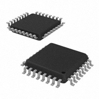
200-MHz clock support LVPECL or LVCMOS/LVTTL clock input LVCMOS/LVTTL compatible inputs 18 clock outputs: drive up to 36 clock lines 60 ps typical output-to-output skew Dual or single supply operation: ❐ 3.3 V core and 3.3 V outputs ❐ 3.3 V core and 2.5 V outputs ❐ 2.5 V core and 2.5 V outputs Pin compatible with MPC940L, MPC9109 Available in Commercial and Industrial temperature 32-pin LQFP package
■ ■ ■
Block Diagram
VDD PECL_CLK PECL_CLK# TCLK TCLK_SEL 0 1 VDDC
18
Q0-Q17
Pin Configuration
VDDC VSS 25 Q0 Q1 Q2 Q3 28 Q4 27 Q5 26
32
31
30
29
VSS VSS TCLK TCLK_SEL PECL_CLK PECL_CLK# VDD VDDC
1 2 3 4 5 6 7 8
CY29940
10 11 12 13 14 15 16 9
24 23 22 21 20 19 18 17
Q6 Q7 Q8 VDD Q9 Q10 Q11 VSS
VSS
VDDC
Q17
Q16
Q15
Q14
Q13
Q12
Cypress Semiconductor Corporation Document #: 38-07283 Rev. *E
•
198 Champion Court
•
San Jose, CA 95134-1709
• 408-943-2600 Revised May 11, 2011
[+] Feedback
�CY29940
Pin Description[1]
Pin 5 6 3 9, 10, 11, 13, 14, 15, 18, 19, 20, 22, 23, 24, 26, 27, 28, 30, 31, 32 4 8, 16, 29 7, 21 1, 2, 12, 17, 25 Name PECL_CLK PECL_CLK# TCLK Q(17:0) VDDC PWR I/O I, PU I, PD I, PD O PECL Input Clock PECL Input Clock External Reference/Test Clock Input Clock Outputs Description
TCLK_SEL VDDC VDD VSS
I, PD
Clock Select Input. When LOW, PECL clock is selected and when HIGH TCLK is selected. 3.3 V or 2.5 V Power Supply for Output Clock Buffers 3.3 V or 2.5 V Power Supply Common Ground
Note 1. PD = Internal Pull-Down, PU = Internal Pull-up
Document #: 38-07283 Rev. *E
Page 2 of 10
[+] Feedback
�CY29940
Maximum Ratings[2]
Maximum Input Voltage Relative to VSS ............. VSS – 0.3 V Maximum Input Voltage Relative to VDD............. VDD + 0.3 V Storage Temperature ................................ –65 C to +150 C Operating Temperature............................... –40 C to +85 C Maximum ESD Protection .............................................. 2 kV Maximum Power Supply................................................ 5.5 V Maximum Input Current ............................................. ±20 mA This device contains circuitry to protect the inputs against damage due to high static voltages or electric field; however, precautions should be taken to avoid application of any voltage higher than the maximum rated voltages to this circuit. For proper operation, Vin and Vout should be constrained to the range: VSS < (Vin or Vout) < VDD Unused inputs must always be tied to an appropriate logic voltage level (either VSS or VDD).
DC Parameters[2]
VDD = 3.3 V ± 5% or 2.5 V ± 5%, VDDC = 3.3 V ± 5% or 2.5 V ± 5%, TA = –40 C to +85 C Parameter VIL VIH IIL IIH VPP VCMR VOL VOH IDDQ IDD Description Input Low Voltage Input High Voltage Input Low Current[3] Input High Current[3] Peak-to-Peak Input Voltage PECL_CLK Common Mode Range[4] PECL_CLK Output Low Output High Voltage[5, 6, 7] Voltage[5, 6, 7] VDD = 3.3 V VDD = 2.5 V IOL = 20 mA IOH = –20 mA, VDDC = 3.3 V IOH = –20 mA, VDDC = 2.5 V Quiescent Supply Current Dynamic Supply Current VDD = 3.3 V, Outputs @ 150 MHz, CL = 15 pF VDD = 3.3 V, Outputs @ 200 MHz, CL = 15 pF VDD = 2.5 V, Outputs @ 150 MHz, CL = 15 pF VDD = 2.5 V, Outputs @ 200 MHz, CL = 15 pF Zout Cin Output Impedance Input Capacitance VDD = 3.3 V VDD = 2.5 V Conditions Min VSS 2.0 – – 500 VDD – 1.4 VDD – 1.0 – 2.4 1.8 – – – – – 8 10 – Typ – – – – – – – – – – 5 285 335 200 240 12 15 4 Max 0.8 VDD –200 200 1000 VDD – 0.6 VDD – 0.6 0.5 – – 7 – – – – 16 20 – pF Unit V V µA µA mV V V V V V mA mA
Notes 2. Multiple Supplies: The Voltage on any input or I/O pin cannot exceed the power pin during power-up. Power supply sequencing is not required. 3. Inputs have pull-up/pull-down resistors that effect input current. 4. The VCMR is the difference from the most positive side of the differential input signal. Normal operation is obtained when the “High” input is within the VCMR range and the input lies within the VPP specification. Driving series or parallel terminated 50 (or 50 to VDD/2) transmission lines 5. Outputs driving 50 transmission lines. 6. See Figure 1 on page 5 and Figure 2 on page 5. 7. 50% input duty cycle.
Document #: 38-07283 Rev. *E
Page 3 of 10
[+] Feedback
�CY29940
AC Parameters[8]
VDD = 3.3 V ± 5% or 2.5 V ± 5%, VDDC = 3.3 V ± 5% or 2.5 V ± 5%, TA = –40 C to +85 C Parameter Fmax tPD Description Input Frequency PECL_CLK to Q Delay[9, 10, 11] 150 MHz VDD = 3.3 V, 85 C VDD = 3.3 V, 70 C VDD = 2.5 V, 85 C VDD = 2.5 V, 70 C tPD LVCMOS to Q Delay[9, 10, 11] 150 MHz VDD = 3.3 V, 85 C VDD = 3.3 V, 70 C VDD = 2.5 V, 85 C VDD = 2.5 V, 70 C tJ FoutDC Tskew Tskew(pp) Tskew(pp) Tskew(pp) tR/tF Total Jitter Output Duty Cycle[9, 10, 12] VDD = 3.3 V @ 150 MHz FCLK < 134 MHz FCLK > 134 MHz Output-to-Output Skew[9, 10] Part-to-Part Skew[13] Part-to-Part Skew[13] Part to Part Skew[14] Output Clocks Rise/Fall Time[9, 10] VDD = 3.3 V VDD = 2.5 V PECL, VDDC = 3.3 V PECL, VDDC = 2.5 V TCLK, VDDC = 3.3 V TCLK, VDDC = 2.5 V PECL_CLK TCLK 0.7 V to 2.0 V, VDDC = 3.3 V 0.5 V to 1.8 V, VDDC = 2.5 V Conditions – tPHL tPLH tPHL tPLH tPHL tPLH tPHL tPLH tPHL tPLH tPHL tPLH tPHL tPLH tPHL tPLH Min – 2.0 2.1 1.9 2.0 2.5 2.6 2.5 2.6 1.9 2.0 1.8 1.8 2.5 2.5 2.3 2.3 – – – – – – – – – – – 0.3 0.3 Typ – – – – – – – – – – – – – – – – – – – – 60 – – – – – – – – – Max 200 3.2 3.4 3.1 3.2 5.2 5 5 5 3 3.2 2.9 3.1 4 4 3.8 3.8 10 55 60 150 200 1.4 2.2 1.2 1.7 850 750 1.1 1.2 ns ps ns ns ps ps % ns Unit MHz ns
Notes 8. Parameters are guaranteed by design and characterization. Not 100% tested in production. All parameters specified with loaded outputs. 9. Outputs driving 50 transmission lines. 10. See Figure 1 on page 5 and Figure 2 on page 5. 11. Parameters tested @ 150 MHz. 12. 50% input duty cycle. 13. Across temperature and voltage ranges, includes output skew. 14. For a specific temperature and voltage, includes output skew.
Document #: 38-07283 Rev. *E
Page 4 of 10
[+] Feedback
�CY29940
Figure 1. LVCMOS_CLK CY29940 Test Reference for VCC = 3.3 V and VCC = 2.5 V
CY29940 DUT
Pulse Generator Z = 50 ohm Zo = 50 ohm RT = 50 ohm Zo = 50 ohm
RT = 50 ohm
VTT
VTT
Figure 2. PECL_CLK CY29940 Test Reference for VCC = 3.3 V and VCC = 2.5 V
Zo = 50 ohm Differential Pulse Generator Z = 50 ohm
CY29940 DUT
Zo = 50 ohm
Zo = 50 ohm RT = 50 ohm RT = 50 ohm
VTT
VTT
Figure 3. Propagation Delay (TPD) Test Reference
PECL_CLK PECL_CLK
VPP
VCMR
VCC
Q
VCC /2
tPD
GND
Figure 4. LVCMOS Propagation Delay (TPD) Test Reference
VCC VCC /2 GND VCC
LVCMOS_CLK
Q
VCC /2
tPD
GND
Document #: 38-07283 Rev. *E
Page 5 of 10
[+] Feedback
�CY29940
Figure 5. Output Duty Cycle (FoutDC)
VCC
tP
T0
VCC /2 GND
DC = tP / T0 x 100%
Figure 6. Output-to-Output Skew tsk(0)
VCC VCC /2 GND VCC VCC /2
tSK(0)
Ordering Information
Part Number Pb-free
CY29940AXI CY29940AXIT CY29940AXC CY29940AXCT 32-pin LQFP 32-pin LQFP – Tape and Reel 32-pin LQFP 32-pin LQFP – Tape and Reel
GND
Package Type
Production Flow
Industrial, –40 C to +85 C Industrial, –40 C to +85 C Commercial, 0 C to 70 C Commercial, 0C to 70 C
Ordering Code Definitions
CY 29940 A X X T
T = Tape and Reel; blank = Tube Temperature Range: X = C or I C = Commercial; I = Industrial Pb-free Package: A = 32-pin LQFP Base part number Company ID: CY = Cypress
Document #: 38-07283 Rev. *E
Page 6 of 10
[+] Feedback
�CY29940
Package Drawing and Dimensions
Figure 7. 32-pin TQFP 7 × 7 × 1.4 mm A32.14
51-85088 *C
Document #: 38-07283 Rev. *E
Page 7 of 10
[+] Feedback
�CY29940
Acronyms
Acronym
ESD I/O LQFP LVCMOS LVPECL LVTTL TQFP input/output low-profile quad flat package low voltage complementary metal oxide semiconductor low-voltage positive emitter-coupled logic low-voltage transistor-transistor logic thin quad flat pack
Document Conventions
Description
Units of Measure
Symbol
°C kV MHz µA mA mm mV ns % pF ps V W degree Celsius kilo Volts Mega Hertz micro Amperes milli Amperes milli meter milli Volts nano seconds ohms percent pico Farad pico seconds Volts Watts
electrostatic discharge
Unit of Measure
Document #: 38-07283 Rev. *E
Page 8 of 10
[+] Feedback
�CY29940
Document History Page
Document Title: CY29940, 2.5 V or 3.3 V, 200-MHz, 1:18 Clock Distribution Buffer Document Number: 38-07283 REV.
** *A
ECN NO.
111094 116776
Issue Date
02/01/02 08/15/02
Orig. of Change
BRK HWT New data sheet
Description of Change
Incorporate results of final characterization using corporate methods, added output impedance on page 3 and added output duty cycle on page 4. Add commercial temperature range in the ordering information on page 6. Add power up requirements to maximum rating information Add typical value for output-to-output skew Add Lead-free devices Removed inactive parts from Ordering Information. Updated package diagram. Added Ordering Code Definitions. Added Acronyms and Units of Measure. Updated in new template.
*B *C *D *E
122875 448379 2899304 3254185
12/21/02 See ECN 03/25/10 05/11/2011
RBI RGL BASH/KVM CXQ
Document #: 38-07283 Rev. *E
Page 9 of 10
[+] Feedback
�CY29940
Sales, Solutions, and Legal Information
Worldwide Sales and Design Support
Cypress maintains a worldwide network of offices, solution centers, manufacturer’s representatives, and distributors. To find the office closest to you, visit us at Cypress Locations.
Products
Automotive Clocks & Buffers Interface Lighting & Power Control Memory Optical & Image Sensing PSoC Touch Sensing USB Controllers Wireless/RF cypress.com/go/automotive cypress.com/go/clocks cypress.com/go/interface cypress.com/go/powerpsoc cypress.com/go/plc cypress.com/go/memory cypress.com/go/image cypress.com/go/psoc cypress.com/go/touch cypress.com/go/USB cypress.com/go/wireless
PSoC Solutions
psoc.cypress.com/solutions PSoC 1 | PSoC 3 | PSoC 5
© Cypress Semiconductor Corporation, 2002-2011. The information contained herein is subject to change without notice. Cypress Semiconductor Corporation assumes no responsibility for the use of any circuitry other than circuitry embodied in a Cypress product. Nor does it convey or imply any license under patent or other rights. Cypress products are not warranted nor intended to be used for medical, life support, life saving, critical control or safety applications, unless pursuant to an express written agreement with Cypress. Furthermore, Cypress does not authorize its products for use as critical components in life-support systems where a malfunction or failure may reasonably be expected to result in significant injury to the user. The inclusion of Cypress products in life-support systems application implies that the manufacturer assumes all risk of such use and in doing so indemnifies Cypress against all charges. Any Source Code (software and/or firmware) is owned by Cypress Semiconductor Corporation (Cypress) and is protected by and subject to worldwide patent protection (United States and foreign), United States copyright laws and international treaty provisions. Cypress hereby grants to licensee a personal, non-exclusive, non-transferable license to copy, use, modify, create derivative works of, and compile the Cypress Source Code and derivative works for the sole purpose of creating custom software and or firmware in support of licensee product to be used only in conjunction with a Cypress integrated circuit as specified in the applicable agreement. Any reproduction, modification, translation, compilation, or representation of this Source Code except as specified above is prohibited without the express written permission of Cypress. Disclaimer: CYPRESS MAKES NO WARRANTY OF ANY KIND, EXPRESS OR IMPLIED, WITH REGARD TO THIS MATERIAL, INCLUDING, BUT NOT LIMITED TO, THE IMPLIED WARRANTIES OF MERCHANTABILITY AND FITNESS FOR A PARTICULAR PURPOSE. Cypress reserves the right to make changes without further notice to the materials described herein. Cypress does not assume any liability arising out of the application or use of any product or circuit described herein. Cypress does not authorize its products for use as critical components in life-support systems where a malfunction or failure may reasonably be expected to result in significant injury to the user. The inclusion of Cypress’ product in a life-support systems application implies that the manufacturer assumes all risk of such use and in doing so indemnifies Cypress against all charges. Use may be limited by and subject to the applicable Cypress software license agreement.
Document #: 38-07283 Rev. *E
Revised May 11, 2011
Page 10 of 10
All products and company names mentioned in this document may be the trademarks of their respective holders.
[+] Feedback
�


 工商网监
湘ICP备2023018690号
工商网监
湘ICP备2023018690号
