CY29976
3.3V, 125-MHz, Multi-Output Zero Delay Buffer
Features
■
Output frequency up to 125 MHz
®
®
■
Spread spectrum compatible
■
Supports PowerPC , and Pentium processors
■
Glitch-free output clocks transitioning
■
12 clock outputs: frequency configurable
■
3.3V power supply
■
Configurable Output Disable
■
Pin compatible with SC973X
■
Two reference clock inputs for dynamic toggling
■
Industrial temperature range: –40°C to +85°C
■
Oscillator or PECL reference input
■
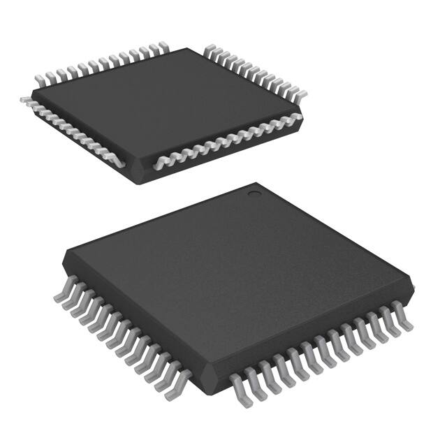
52-Pin TQFP package
Table 1. Frequency Table[1]
VC0_SEL
FB_SEL2
FB_SEL1
FB_SEL0
FVCO
0
0
0
0
0
0
0
0
1
1
1
1
1
1
1
1
0
0
0
0
1
1
1
1
0
0
0
0
1
1
1
1
0
0
1
1
0
0
1
1
0
0
1
1
0
0
1
1
0
1
0
1
0
1
0
1
0
1
0
1
0
1
0
1
8x
12x
16x
20x
8x
12x
16x
20x
4x
6x
8x
10x
4x
6x
8x
10x
Note
1. x = the reference input frequency, 200MHz < FVCO < 480MHz.
Cypress Semiconductor Corporation
Document #: 38-07413 Rev. *B
•
198 Champion Court
•
San Jose, CA 95134-1709
•
408-943-2600
Revised September 09, 2008
[+] Feedback
�CY29976
Logic Block Diagram
P E C L
P E C L_
V C O
P L
R E F
_C LK
C LK #
_S E L
L_E N
_S E L
D
T C LK 0
T C LK 1
T C LK _S E L
P hase
D e te c to r
0
1
Q
0
1
V C O
S ync
F rz
Q A 0
Q A 1
LP F
Q A 2
Q A 3
F B _ IN
D
Q
S ync
F rz
Q B 0
Q B 1
Q B 2
Q B 3
M R # /O E
Q
S ync
F rz
D
Q
S ync
F rz
D
Q
S ync
F rz
F B _O U T
D
Q
S ync
F rz
S Y N C
D
P o w e r-O n
R eset
/2 , /6 , /4 , /1 2
S E L A (0 ,1 )
2
S E L B (0 ,1 )
2
Q C 1
/2 , /6 , /4 , /1 0
/8 , /2 , /6 , /4
S E L C (0 ,1 )
2
F B _ S E L (0 :2 )
3
Q C 0
Q C 2
Q C 3
/4 , /6 , /8 , /1 0
S y n c P u ls e
D a ta G e n e ra to r
S C LK
S D A T A
O u tp u t D is a b le
C ir c u itr y
12
IN V _ C L K
Pinouts
SELB1
SELB0
SELA1
SELA0
QA3
VDDC
QA2
VSS
QA1
VDDC
QA0
VSS
VCO_SEL
52 51 50 49 48 47 46 45 44 43 42 41 40
VSS
MR#/OE
SCLK
SDATA
FB_SEL2
PLL_EN
REF_SEL
TCLK_SEL
TCLK0
TCLK1
PECL_CLK
PECL_CLK#
VDD
1
2
3
4
5
6
7
8
9
10
11
12
13
39
38
37
36
35
34
33
32
31
30
29
28
27
CY29976
VSS
QB0
VDDC
QB1
VSS
QB2
VDDC
QB3
FB_IN
VSS
FB_OUT
VDDC
FB_SEL0
14 15 16 17 18 19 20 21 22 23 24 25 26
FB_SEL1
SYNC
VSS
QC0
VDDC
QC1
SELC0
SELC1
QC2
VDDC
QC3
VSS
INV_CLK
Document #: 38-07413 Rev. *B
Page 2 of 9
[+] Feedback
�CY29976
Pin Definitions[2]
Pin No.
Pin Name
PWR
IO
Type
Description
11
PECL_CLK
I
PU
PECL Clock Input.
12
PECL_CLK#
I
PD
PECL Clock Input.
9
TCLK0
I
PU
External Reference/Test Clock Input.
10
TCLK1
I
PU
External Reference/Test Clock Input.
44, 46, 48, 50
QA(3:0)
VDDC
O
Clock Outputs. See Table 2 on page 4 for frequency selections.
32, 34, 36, 38
QB(3:0)
VDDC
O
Clock Outputs. See Table 2 on page 4 for frequency selections.
16, 18, 21, 23
QC(3:0)
VDDC
O
Clock Outputs. See Table 2 on page 4 for frequency selections.
O
Feedback Clock Output. Connect to FB_IN for normal operation. The
divider ratio for this output is set by FB_SEL(0:2). See Table 1 on page
1. A bypass delay capacitor at this output controls Input Reference/
Output Banks phase relationships.
O
Synchronous Pulse Output. This output is used for system synchronization. The rising edge of the output pulse is in sync with both the rising
edges of QA (0:3) and QC(0:3) output clocks regardless of the divider
ratios selected.
29
FB_OUT
VDDC
25
SYNC
42, 43
SELA(1,0)
I
PU
Frequency Select Inputs. These inputs select the divider ratio at
QA(0:3) outputs. See Table 2 on page 4.
40, 41
SELB(1,0)
I
PU
Frequency Select Inputs. These inputs select the divider ratio at
QB(0:3) outputs. See Table 2 on page 4.
19, 20
SELC(1,0)
I
PU
Frequency Select Inputs. These inputs select the divider ratio at
QC(0:3) outputs. See Table 2 on page 4.
5, 26, 27
FB_SEL(2:0)
I
PU
Feedback Select Inputs. These inputs select the divide ratio at FB_OUT
output. See Table 1 on page 1.
52
VCO_SEL
I
PU
VCO Divider Select Input. When set LOW, the VCO output is divided
by 2. When set HIGH, the divider is bypassed. See Table 1 on page 1.
31
FB_IN
I
PU
Feedback Clock Input. Connect to FB_OUT for accessing the PLL.
6
PLL_EN
I
PU
PLL Enable Input. When asserted HIGH, PLL is enabled. When LOW,
PLL is bypassed.
7
REF_SEL
I
PU
Reference Select Input. When HIGH, the PECL clock is selected. When
LOW, TCLK (0,1) is the reference clock.
8
TCLK_SEL
I
PU
TCLK Select Input. When LOW, TCLK0 is selected and when HIGH
TCLK1 is selected.
2
MR#/OE
I
PU
Master Reset/Output Enable Input. When asserted LOW, resets all of
the internal flip-flops and also disables all of the outputs. When pulled
HIGH, releases the internal flip-flops from reset and enables all of the
outputs.
14
INV_CLK
I
PU
Inverted Clock Input. When set HIGH, QC(2,3) outputs are inverted.
When set LOW, the inverter is bypassed.
3
SCLK
I
PU
Serial Clock Input. Clocks data at SDATA into the internal register.
PU
Serial Data Input. Input data is clocked to the internal register to
enable/disable individual outputs. This provides flexibility in power
management.
4
SDATA
17, 22, 28,
33,37, 45, 49
VDDC
13
VDD
1, 15, 24, 30,
35, 39, 47, 51
VSS
VDDC
I
3.3V Power Supply for Output Clock Buffers.
3.3V Supply for PLL
Common Ground
Note
2. A bypass capacitor (0.1μF) must be placed as close as possible to each positive power (