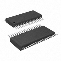
ComLink™ Series CY2DP818
1:8 Clock Fanout Buffer
Features
• • • • • • • • • • • • Low-voltage operation VDD = 3.3V 1:8 fanout Single-input-configurable for LVDS, LVPECL, or LVTTL 8 pair of LVPECL outputs Drives a 50-ohm load Low input capacitance Low output skew Low propagation delay Typical (tpd < 4 ns) Industrial versions available Package available include: TSSOP Does not exceed Bellcore 802.3 standards Operation at ⇒ 350 MHz–700 Mbps
Description
This Cypress series of network circuits are produced using advanced 0.35-micron CMOS technology, achieving the industry’s fastest logic. The Cypress CY2DP818 fanout buffer features a single LVDS or a single-ended LVTTL-compatible input and eight LVPECL output pairs. Designed for data-communications clock-management applications, the large fanout from a single input reduces loading on the input clock. The CY2DP818 is ideal for both level translations from single-ended to LVPECL and/or for the distribution of LVPECL-based clock signals. The Cypress CY2DP818 has configurable input functions. The input is user configurable via the Inconfig pin for single ended or differential input.
Block Diagram
Q1A Q1B
Pin Configuration
Q2A Q2B
INPUT
(LVPECL / LVDS / LVTTL)
Q4A INPUT A INPUT B Q4B Q5A
CY2DP818
Q3A Q3B
InConfig
Q5B Q6A Q6B
Q7A Q7B
GND V DD VDD VDD VDD VDD InConfig VDD GND INPUT A INPUT B GND VDD VDD VDD VDD VDD GND GND
1 2 3 4 5 6 7 8 9 10 11 12 13 14 15 16 17 18 19
38 37 36 35 34 33 32 31 30 29 28 27 26 25 24 23 22 21 20
GND Q1A Q1B Q2A Q2B Q3A Q3B Q4A Q4B VDD Q5A Q5B Q6A Q6B Q7A Q7B Q8A Q8B GND
Q8A Q8B
38-pin TSSOP
OUTPUT
(LVPECL)
Cypress Semiconductor Corporation Document #: 38-07061 Rev. *A
•
3901 North First Street
•
San Jose
•
CA 95134
• 408-943-2600 Revised July 9, 2002
�ComLink™ Series CY2DP818
Pin Description
Pin Number 1, 9,12,18,19,20,38 2,3,4,5,6,8, 13,14,15,16,17,29 10,11 VDD Input A, Input B Pin Name GND Pin Standard Interface POWER POWER Default: LVPECL/LDVS Optional: LVTTL/LVCMOS single pin LVPECL Ground Power Supply Differential input pair or single line. LVPECL/LVDS default. See InConfig, below. Differential Outputs Description
37, 36,35,34, 33,32,31, 30, 28,27,26,25, 24,23,22,21 7
Q1(A,B), Q2(A,B) Q3(A,B), Q4(A,B) Q5(A,B), Q6(A,B) Q7(A,B), Q8(A,B) InConfig
LVTTL/LVCMOS
Converts inputs from the default LVPECL/LVDS (logic = 0) To LVTTL/LVCMOS (logic = 1) See Figure 4 and Figure 5 for additional Information
Maximum Ratings[1]
Storage Temperature: ................................ –65°C to + 150°C Ambient Temperature:................................... –40°C to +85°C Supply Voltage to Ground Potential (Inputs and VCC only)....................................... –0.3V to 4.6V Table 1. Power Supply Characteristics Parameter ICCD Description Dynamic Power Supply Current Test Conditions VDD = Max. Input toggling 50% Duty Cycle, Outputs Open VDD = Max. Input toggling 50% Duty Cycle, Outputs 50 ohms fL=100 MHz Min. Typ. 1.5 Max. 2.0 Unit mA/MHz Supply Voltage to Ground Potential (Outputs only) ........................................ –0.3V to VDD + 0.3V DC Input Voltage ................................... –0.3V to VDD + 0.3V DC Output Voltage................................. –0.3V to VDD + 0.9V Power Dissipation........................................................ 0.75W
IC
Total Power Supply Current
350
mA
IC Core
Core current when output loads are VDD = Max. Input toggling 50% Duty Cycle, Outputs disabled Disabled, not connected to VTT fL=100 MHz
50
mA
Table 2. Input Receiver Configuration for Differential or LVTTL/LVCMOS INCONFIG Pin 7 Binary Value 1 0 Input Receiver Family LVTTL in LVCMOS LVDS LVPECL Input Receiver Type Single-ended, non-inverting, inverting, void of bias resistors Low-voltage differential signaling Low-voltage pseudo (positive) emitter coupled logic
Notes: 1. Stresses greater than those listed under absolute maximum ratings may cause permanent damage to the device. This is intended to be a stress rating only and functional operation of the device at these or any other conditions above those indicated in the operation sections of this specification is not implied. Exposure to absolute maximum rating conditions for extended periods may affect reliability.
Document #: 38-07061 Rev. *A
Page 2 of 8
�ComLink™ Series CY2DP818
Table 3. Function Control of the TTL Input Logic used to Accept or Invert the Input Signal LVTTL/LVCMOS Input Logic Input Condition Ground VCC Ground VCC Input B (–) Pin 11 Input A (+) Pin 10 Input B (–) Pin 11 Input A (+) Pin 10 Input A (+) Pin 10 Input B (–) Pin 11 Input A (+) Pin 10 Input B (–) Pin 11 Parameter VID VIC VIH VIL IIH IIL II Parameter VID VIH VIL IIH IIL II VCM Parameter VIH VIL IIH IIL II VIK VH Description Magnitude of Differential Input Voltage Common-mode of Differential Input VoltageIVIDI (min. and max.) Input High Voltage Input Low Voltage Input High Current Input Low Current Input High Current Description Differential Input Voltage p-p Input High Voltage Input Low Voltage Input High Current Input Low Current Input High Current Common-mode Voltage Description Input High Voltage Input Low Voltage Input High Current Input Low Current Input High Current Clamp Diode Voltage Input Hysteresis Conditions Guaranteed Logic High Level Guaranteed Logic Low Level VDD = Max VDD = Max VDD = Max., VIN = VDD(Max) VDD = Min., IIN = –18mA –0.7 80 VIN = 2.7V VIN = 0.5V Min. 2 0.8 1 –1 20 –1.2 Typ. Guaranteed Logic High Level Guaranteed Logic Low Level VDD = Max. VDD = Max. VDD = Max., VIN = VDD(Max.) Conditions Guaranteed Logic High Level Guaranteed Logic High Level Guaranteed Logic Low Level VDD = Max. VDD = Max. VDD = Max., VIN = VDD(Max.) VIN = VDD VIN = VSS Min. 400 2.15 1.5 ±10 ±10 Typ. VIN = VDD VIN = VSS ±10 ±10 Input Conditions True Min. 100 Typ. Max. 600 Unit mV V V 0.8 ±20 ±20 ±20 Max. 2600 2.4 1.8 ±20 ±20 ±20 225 Max. V µA µA µA Unit mV V V µA µA µA mV Units V V µA µA µA V mV Input Invert Input Invert Input True Input Logic Output Logic Q Pins, Q1A or Q1
Table 4. DC Electrical Characteristics: 3.3V–LVDS Input
IVIDI/2 2.4–(IVIDI/2) 2
Table 5. DC Electrical Characteristics: 3.3V–LVPECL Input
Table 6. DC Electrical Characteristics: 3.3V–LVTTL/LVCMOS Input
Document #: 38-07061 Rev. *A
Page 3 of 8
�ComLink™ Series CY2DP818
Table 7. DC Electrical Characteristics: 3.3V–LVPECL Output Parameter VOD VOC Rise Time Fall Time VOH VOL IOS Output High Voltage Output Low Voltage Short Circuit Current VDD = Min., VIN = VIH or VIL VDD = Min., VIN = VIH or VIL User defined by VTT RTT. VDD = Max, VOUT = GND IOH = –12 mA 2.1 0.8 –125 3.0 1.3 –150 V V mA Description Conditions RL = 50 ohm RL = 50 ohm 300 Min. 1000 Typ. Max. 3600 300 1200 Unit mV mV ps Driver Differential Output VDD = Min., VIN = VIH or VIL voltage p-p Driver common-mode p-p VDD = Min., VIN = VIH or VIL Differential 20% to 80%
CL–10 pF RL and CL to GND RL = 50 ohm
Driver Design
Table 8. AC Switching Characteristics @ 3.3 V (VDD = 3.3V ±5%, Temperature = –40°C to +85°C) Parameter tPLH tPHL TPE TPD tSK(0) tSK(p) tSK(t) Description Propagation Delay – Low to High Propagation Delay – High to Low Enable (EN) to functional operation Functional operation to Disable Output Skew: Skew between outputs of the same package (in phase) Pulse Skew: Skew between opposite transitions of the same output (tPHL–tPLH) Package Skew: Skew between outputs of different packages at the same power supply voltage, temperature and package type. Same input signal level and output load. VID = 100 mV 0.2 1 Conditions VOD = 100 mV Min. 3 3 Typ. Max. Unit 4 4 5 5 6 5 0.2 ns ns ns ns ns ns ns
Table 9. High-frequency Parametrics Parameter Fmax Description Maximum frequency VDD = 3.3V Conditions 45%–55% duty cycle Standard load circuit Min. Typ. Max. 350 Unit MHz
Document #: 38-07061 Rev. *A
Page 4 of 8
�ComLink™ Series CY2DP818
A
Pulse Generator
TPA
150 10pF B 150 GND
50
TPC VDD-2V
50
TPB
Standard Termination
V1A
1 .2 V C M
1.4 V
0 V D iffe re n tia l
V1B V0Y
1 .2 V C M
1.0 V 1.4 V
0 V D iffe re n tia l
V0Z
T P LH T PHL
1.0 V
80% 0 V D iffe re n tia l V0Y V0Z t R t F 20%
Figure 1. Differential Receiver to Driver Propagation Delay and Driver Transition Time[2,3,4,5]
A
Pulse Generator
TPA
150 B 150 GND
50
TPC
50
TPB
VOC
VOD
Standard Termination
VI(A) VI(B)
2.0V 1.6V
Next Device
Figure 2. Test Circuit and Voltage Definitions for the Driver Common-Mode Output Voltage[2,3,4,5]
Notes: 2. All input pulses are supplied by a frequency generator with the following characteristics: tR and tF ≤ 1 ns; pulse rerate = 50 Mpps; pulse width = 10 ± 0.2 ns. 3. RL = 50 ohm ± 1%; Zline = 50 ohm 6”. 4. CL includes instrumentation and fixture capacitance within 6 mm of the UT. 5. TPA and B are used for prop delay and Rise/Fall measurements. TPC is used for VOC measurements only and is otherwise connected to VDD – 2.
Document #: 38-07061 Rev. *A
Page 5 of 8
�ComLink™ Series CY2DP818
A
Pulse Generator
TPA
150 10pF B 150 GND
50
TPC VDD-2V
50
TPB
Standard Termination
VI(A) VI(B)
1.4V 1.0V
100% 80%
0.0V
20% 0%
tF
tR
Figure 3. Test Circuit and Voltage Definitions for the Differential Output Signal[2,3,4,5]
INPUT A
LVCM OS / LVTTL
INPUT B GND
LVPECL & LVDS
In C o n fig
InConfig
0
1
L V D S /L V P E C L
LVTTL/LVCMOS
Figure 4. [6] Figure 5. [7]
Notes: 6. See Table 3. 7. LVPECL or LVDS differential input value.
Document #: 38-07061 Rev. *A
Page 6 of 8
�ComLink™ Series CY2DP818
Ordering Information
Part Number CY2DP818ZI CY2DP818ZIT CY2DP818ZC CY2DP818ZCT Package Type 38-pin TSSOP 38-pin TSSOP–Tape and Reel 38-pin TSSOP 38-pin TSSOP–Tape and Reel Product Flow Industrial, –40° to 85°C Industrial, –40° to 85°C Commercial, 0°C to 70°C Commercial, 0°C to 70°C
Package Drawing and Dimensions
38-lead TSSOP (4.40 mm Body) Z38
51-85151-**
ComLink is a trademark of Cypress Semiconductor Corporation. All product and company names mentioned in this document are the trademarks of their respective holders.
Document #: 38-07061 Rev. *A
Page 7 of 8
© Cypress Semiconductor Corporation, 2002. The information contained herein is subject to change without notice. Cypress Semiconductor Corporation assumes no responsibility for the use of any circuitry other than circuitry embodied in a Cypress Semiconductor product. Nor does it convey or imply any license under patent or other rights. Cypress Semiconductor does not authorize its products for use as critical components in life-support systems where a malfunction or failure may reasonably be expected to result in significant injury to the user. The inclusion of Cypress Semiconductor products in life-support systems application implies that the manufacturer assumes all risk of such use and in doing so indemnifies Cypress Semiconductor against all charges.
�ComLink™ Series CY2DP818
Document Title: CY2DP818 1:8 Clock Fanout Buffer Document Number: 38-07061 REV. ** *A ECN NO. 107086 115913 Issue Date 06/07/01 07/11/02 Orig. of Change IKA CTK New Data Sheet IC, VCM, VOC, Rise/Fall Time Fmax (20) Description of Change
Document #: 38-07061 Rev. *A
Page 8 of 8
�