CY2XF23
High Performance LVDS Oscillator with Frequency Margining - I2C Control
High Performance LVDS Oscillator with Frequency Margining - I2C Control
Features
■ ■ ■ ■ ■ ■ ■ ■ ■ ■
Functional Description
The CY2XF23 is a high-performance and high-frequency XO. It uses a Cypress proprietary low-noise PLL to synthesize the frequency from an integrated crystal. The output frequency can be changed using the I2C bus serial interface, allowing easy frequency margin testing in applications. The CY2XF23 is available as a factory-configured device or as a field-programmable device. Factory configured devices are configured for general use (see Standard and Application-Specific Factory Configurations) or they can be customer specific.
Low jitter crystal oscillator (XO) Less than 1 ps typical root mean square (RMS) phase jitter Low-voltage differential signaling (LVDS) output Output frequency from 50 MHz to 690 MHz Frequency margining through I2C bus Factory-configured or field-programmable Integrated phase-locked loop (PLL) Pb-free package: 5.0 × 3.2 mm leadless chip carrier (LCC) Supply voltage: 3.3 V or 2.5 V Commercial and industrial temperature ranges
Logic Block Diagram
4 CRYSTAL OSCILLATOR LOW-NOISE PLL CLK OUTPUT DIVIDER 5 CLK#
1 SDA 2 SCL
I 2C INTERFACE
PROGRAMMABLE CONFIGURATION
Cypress Semiconductor Corporation Document Number: 001-53145 Rev. *E
•
198 Champion Court
•
San Jose, CA 95134-1709
• 408-943-2600 Revised April 14, 2011
[+] Feedback
�CY2XF23
Contents
Pinouts .............................................................................. 3 Pin Definitions .................................................................. 3 Standard and Application-Specific Factory Configurations .................................................... 4 Functional Description ..................................................... 4 Configuration Software .................................................... 4 Programming Description ............................................... 5 Field-Programmable CY2XF23F ................................. 5 Factory-Configured CY2XF23 ..................................... 5 Programming Variables ................................................... 5 Output Frequencies ..................................................... 5 Industrial versus Commercial Device Performance .... 5 Memory Map ...................................................................... 5 Serial Interface Protocol and Timing ........................... 5 Device Address ........................................................... 6 Data Valid .................................................................... 6 Data Frame ................................................................. 6 Acknowledge Pulse ..................................................... 6 Write Operations ............................................................... 6 Writing Individual Bytes ............................................... 6 Writing Multiple Bytes .................................................. 6 Read Operations ............................................................... 6 Current Address Read ................................................. 6 Random Read ............................................................. 6 Sequential Read .......................................................... 6 Absolute Maximum Conditions ....................................... 8 Operating Conditions ....................................................... 8 DC Electrical Characteristics .......................................... 9 AC Electrical Characteristics ........................................ 10 I2C Bus Timing Specifications ...................................... 10 Switching Waveforms .................................................... 11 Termination Circuits ....................................................... 12 Ordering Information ...................................................... 12 Possible Configurations ............................................. 12 Package Drawings and Dimensions ............................. 13 Acronyms ........................................................................ 14 Document Conventions ................................................. 14 Units of Measure ....................................................... 14 Document History Page ................................................. 15 Sales, Solutions, and Legal Information ...................... 16 Worldwide Sales and Design Support ....................... 16 Products .................................................................... 16 PSoC Solutions ......................................................... 16
Document Number: 001-53145 Rev. *E
Page 2 of 16
[+] Feedback
�CY2XF23
Pinouts
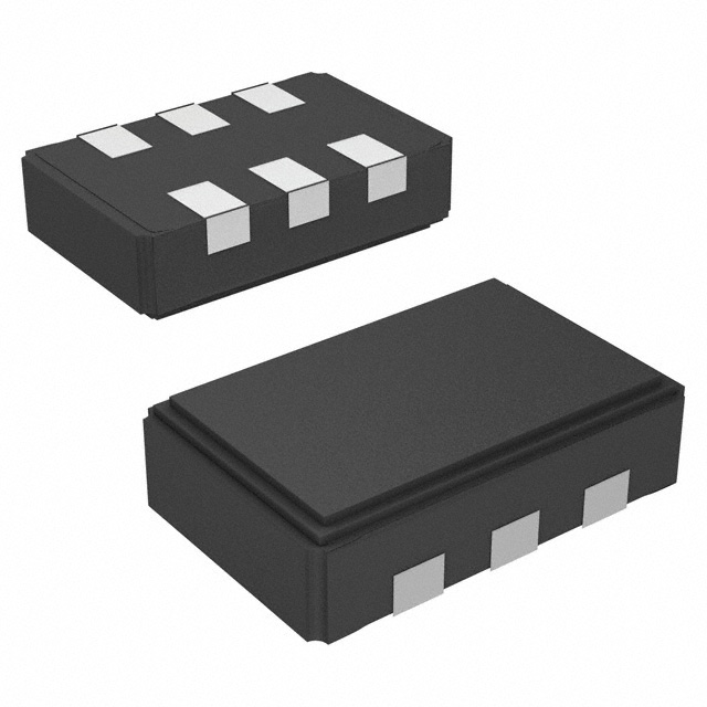
Figure 1. Pin Diagram – 6-pin Ceramic LCC
SDA 1 SCLK 2 VSS 3
6 VDD 5 CLK# 4 CLK
Pin Definitions
6-pin Ceramic LCC Pin 1 2 4, 5 6 3 Name SDA SCLK CLK, CLK# VDD VSS I/O Type I/O CMOS input LVDS output Power Power I2C serial data I2C serial clock Differential output clock Supply voltage: 2.5 V or 3.3 V Ground Description
Document Number: 001-53145 Rev. *E
Page 3 of 16
[+] Feedback
�CY2XF23
Standard and Application-Specific Factory Configurations
Part Number CY2XF23LXC001T Output Frequency 100.00 MHz (default) 95.00 MHz 103.000007 MHz 104.999993 MHz 78.125 MHz 156.25 MHz 312.50 MHz 625.00 MHz (default) Frequency Word 0 1 2 3 0 1 2 3 RMS Phase Jitter (Random) Offset Range 637 kHz to 10 MHz 637 kHz to 10 MHz 637 kHz to 10 MHz 637 kHz to 10 MHz 1.875 MHz to 20 MHz 1.875 MHz to 20 MHz 1.875 MHz to 20 MHz 1.875 MHz to 20 MHz Jitter (Typical) 0.52 ps – – – 0.37 ps 0.31 ps 0.29 ps 0.31 ps
CY2XF23LXI625T
Functional Description
The CY2XF23 is a PLL-based high-performance clock generator. It uses an internal crystal oscillator as a reference, and outputs one differential LVDS clock. It has an I2C bus serial interface[1], which is used to change the output frequency. The CY2XF23 comes configured for four different frequencies. At power-on, the four configurations are transparently loaded into an internal volatile memory which, in turn, controls the PLL. The user can switch between the four frequencies through the I2C bus. The user can also configure the CY2XF23 with new output frequencies by shifting new data into the internal memory. Frequency margining is a common application for this feature. One frequency is used for the standard operating mode of the device, while additional frequencies are available for margin testing, either during product development or in-system manufacturing test. Note that all configuration changes made using I2C are temporary and are lost when power is removed from the device. At power-on, the device returns to its original state. The configuration for a particular frequency is stored in a 6-byte block of memory, known as a word. The CY2XF23 has four such words, labeled ‘Frequency Word 0’ through ‘Frequency Word 3’. An additional register byte contains a 2-bit field, which selects one of the four frequency words. By writing to this select byte, the user can switch back and forth between the four programmed frequencies. The select byte can be configured to select any of the four frequency words at power-on. When changing the output frequency, the frequency transition is not guaranteed to be smooth. There can be frequency excursions beyond the start frequency and the new frequency.
Glitches and runt pulses are possible, and time must be allowed for the PLL to re-lock. If more than four frequencies are needed, the I2C bus can be used to change any of the four frequency words. When writing frequency words through I2C, users should not change the currently selected word. Instead, write one of the three unselected words before changing the select byte to select that new word. Figure 2 shows how the frequency words are arranged and selected. Figure 2. Frequency Words
Register Address 10h – 15h 16h – 1Bh 1Ch – 21h 22h – 27h 40h Frequency Word 0 Frequency Word 1 Frequency Word 2 Frequency Word 3 Select Byte Bits [1:0]
00 01 10 11 Sel
Control
PLL
Configuration Software
Cypress provides CyClockWizard™ software that enables users to create data values for shifting into the frequency words. This software is required because the algorithm is too complicated to be described here. The user specifies the output frequency. The software then calculates the bit stream for up to four frequency words, as outlined by the register addresses for each word seen in Figure 2.
Note 1. The serial interface is I2C Bus compliant, with the following exceptions: SDA input leakage current, SDA input capacitance, SDA and SCLK are clamped to VDD, setup time, and output hold time.
Document Number: 001-53145 Rev. *E
Page 4 of 16
[+] Feedback
�CY2XF23
Programming Description
The CY2XF23 is a programmable device. Before being used in an application, it must be programmed with the output frequencies and other variables described in Programming Variables on page 5. Two different device types are available, each with its own programming flow. They are described in the following sections. Table 1. Device Programming Variables Variable Output frequency 0 Output frequency 1 Output frequency 2 Output frequency 3 Temperature range (commercial or industrial)
Field-Programmable CY2XF23F
Field programmable devices are shipped unprogrammed and must be programmed before being installed on a printed circuit board (PCB). Customers use CyClockWizard™ software to specify the device configuration and generate a joint electron devices engineering council (JEDEC - extension .jed) programming file. Programming of samples and prototype quantities is available using the CyClockWizard software along with a CY3675-CLKMAKER1 CyClockMaker Clock Programmer Kit with a CY3675-LCC6A socket adapter. Cypress’s value added distribution partners also provide programming services. Field programmable devices are designated with an ‘F’ in the part number. They are intended for quick prototyping and inventory reduction. The software and programmer kit hardware can be downloaded from www.cypress.com by clicking the hyperlinks above.
Memory Map
Five fields can be written via the I2C bus. Four frequency words define the output frequency. As shown in Table 2, each of these words is a 6-byte field. When writing to a frequency word, all six bytes should be written. They may be written either as individual byte writes, or as a block write. The currently selected frequency word should not be written to. All four words are symmetrical, meaning that a 6-byte value that is valid for one word is also valid for any of the other words, and produces the same frequency. The fifth field is the select byte, located at byte address 40h. The value written into the two least significant bits determines the active frequency word. The other bits of the byte are reserved and must be written with the values indicated in the table. Users should never write to any address other than the 25 bytes described here. Table 2. Frequency Words Frequency Word 0 1 2 3 Byte Addresses (hex) 10h to 15h 16h to 1Bh 1Ch to 21h 22h to 27h Word Select (Select Byte 40h) 00 01 10 11
Factory-Configured CY2XF23
For ready-to-use devices, the CY2XF23 is available with no field programming required. Pre-configured devices (see Standard and Application-Specific Factory Configurations) are available for samples or orders, or a request for a custom configuration can be made. All requests are submitted to the local Cypress Field Application Engineer (FAE) or sales representative. After the request is processed, the user receives a new part number, samples, and datasheet with the programmed values. This part number is used for additional sample requests and production orders. The CY2XF23 is one-time programmable (OTP).
Table 3. Register 40h: Select Byte Bits 7:2 1:0 Default Value Name (binary) 000000 Reserved User-defined Description
Programming Variables
Output Frequencies
The CY2XF23 is programmed with up to four independent output frequencies, which are then selected using the I2C interface. The device can synthesize frequencies to a resolution of 1 part per million (ppm), but the actual accuracy of the output frequency is limited by the accuracy of the integrated reference crystal. The CY2XF23 has an output frequency range of 50 MHz to 690 MHz, but the range is not continuous. The CY2XF23 cannot generate frequencies in the ranges of 521 MHz to 529 MHz and 596 MHz to 617 MHz.
Reserved. Always write this value. Word select Selects the Frequency Word to determine the output frequency. 00 selects Word 0; 01 selects Word 1; 10 selects Word 2; 11 selects Word 3.
Serial Interface Protocol and Timing
The CY2XF23 uses pins SDA and SCLK for an I2C bus that operates up to 100 kbits/sec in read or write mode. The CY2XF23 is always a slave on this bus, meaning that it never initiates a bus transaction. The basic write protocol is as follows: Start Bit; 7-bit Device Address (DA); R/W Bit; Slave Clock Acknowledge (ACK); 8-bit Memory Address (MA); ACK; 8-bit Data; ACK; 8-bit Data in MA+1 if desired; ACK; 8-bit Data in MA+2; ACK; and so on, until STOP Bit. The basic serial format is illustrated in Figure 4 on page 7.
Industrial versus Commercial Device Performance
Industrial and commercial devices have different internal crystals. They have a potentially significant impact on performance levels for applications requiring the lowest possible phase noise. CyClockWIzard software allows the user to select between and view the expected performance of both options.
Document Number: 001-53145 Rev. *E
Page 5 of 16
[+] Feedback
�CY2XF23
Device Address
The device address is a 7-bit value. The default serial interface address is 69H. responded to by the STOP condition. When receiving multiple bytes, the CY2XF23 internally increments the register address.
Read Operations
Read operations are initiated the same way as write operations except that the R/W bit of the slave address is set to ‘1’ (HIGH). There are three basic read operations: current address read, random read, and sequential read.
Data Valid
Data is valid when the clock is HIGH, and may only be transitioned when the clock is LOW as illustrated in Figure 5 on page 7.
Data Frame
Every new data frame is indicated by a start and stop sequence, as illustrated in Figure 6 on page 7. START Sequence - Start frame is indicated by SDA going LOW when SCLK is HIGH. Every time a start signal is given, the next 8-bit data must be the device address (seven bits) and a R/W bit, followed by register address (eight bits) and register data (eight bits). STOP Sequence - Stop frame is indicated by SDA going HIGH when SCLK is HIGH. A stop frame frees the bus for writing to another part on the same bus or writing to another random register address.
Current Address Read
The CY2XF23 has an onboard address counter that retains 1 more than the address of the last word access. If the last word written or read was word ‘n’, then a current address read operation would return the value stored in location ‘n+1’. When the CY2XF23 receives the slave address with the R/W bit set to a ‘1’, the CY2XF23 issues an acknowledge and transmits the 8-bit word. The master device does not acknowledge the transfer, but does generate a STOP condition, which causes the CY2XF23 to stop transmission.
Random Read
Through random read operations, the master may access any memory location. To perform this type of read operation, first the word address must be set. This is accomplished by sending the address to the CY2XF23 as part of a write operation. After the word address is sent, the master generates a START condition following the acknowledge. This terminates the write operation before any data is stored in the address, but not before the internal address pointer is set. Next the master reissues the control byte with the R/W byte set to ‘1’. The CY2XF23 then issues an acknowledge and transmits the 8-bit word. The master device does not acknowledge the transfer, but does generate a STOP condition which causes the CY2XF23 to stop transmission.
Acknowledge Pulse
During write mode, the CY2XF23 responds with an Acknowledge (ACK) pulse after every eight bits. This is accomplished by pulling the SDA line LOW during the N*9th clock cycle as illustrated in Figure 7 on page 8. (N = the number of bytes transmitted). After the data packet is sent during read mode, the master generates the acknowledge.
Write Operations
Writing Individual Bytes
A valid write operation must have a full 8-bit register address after the device address word from the master, which is followed by an acknowledge bit from the slave (SDA = 0/LOW). The next eight bits must contain the data word intended for storage. After the data word is received, the slave responds with another acknowledge bit (SDA = 0/LOW), and the master must end the write sequence with a STOP condition.
Sequential Read
Sequential read operations follow the same process as random reads except that the master issues an acknowledge instead of a STOP condition after transmission of the first 8-bit data word. This action results in an incrementing of the internal address pointer, and subsequently output of the next 8-bit data word. By continuing to issue acknowledges instead of STOP conditions, the master may serially read the entire contents of the slave device memory. When the internal address pointer points to the FFh register, after the next increment, the pointer will point to the 00h register.
Writing Multiple Bytes
To write more than one byte at a time, the master does not end the write sequence with a stop condition. Instead, the master can send multiple contiguous bytes of data to be stored. After each byte, the slave responds with an acknowledge bit, just like after the first byte, and accepts data until the acknowledge bit is
Figure 3. Data Transfer Sequence on the Serial Bus SCLK
SDA
START Condition Address or Acknowledge Valid Data may be changed STOP Condition
Document Number: 001-53145 Rev. *E
Page 6 of 16
[+] Feedback
�CY2XF23
Figure 4. Data Frame Architecture
SDA Write
Multiple Contiguous Registers
Start Signal
1 Bit 1 Bit Slave ACK R/W = 0 7-bit Device Address
1 Bit Slave ACK
1 Bit Slave ACK 8-bit Register Data (XXH+1)
1 Bit Slave ACK 8-bit Register Data (XXH+2)
1 Bit Slave ACK 8-bit Register Data (FFH)
1 Bit Slave ACK
1 Bit Slave ACK
1 Bit Slave ACK
8-bit Register Address (XXH)
8-bit Register Data (XXH)
8-bit Register Data (00H) Stop Signal
SDA Read
Current Address Read Start Signal
1 Bit 1 Bit Slave R/W = 1 ACK 7-bit Device Address
1 Bit Slave ACK
1 Bit Master ACK
8-bit Register Data Stop Signal
SDA Read
Multiple Contiguous Registers
Start Signal
1 Bit 1 Bit Slave R/W = 0 ACK 7-bit Device Address
1 Bit Slave ACK
1 Bit Master ACK 8-bit Register Data (XXH)
1 Bit Master ACK 8-bit Register Data (XXH+1)
1 Bit Master ACK 8-bit Register Data (FFH)
1 Bit Master ACK
1 Bit Master ACK
1 Bit Master ACK
8-bit Register Address (XXH)
7-bit Device Address +R/W=1 Repeated Start bit
8-bit Register Data (00H) Stop Signal
Figure 5. Data Valid and Data Transition Periods
Data Valid Transition to next Bit
SDA
tDH
tSU
VIH
CLKHIGH CLKLOW
SCLK
VIL
Figure 6. Start and Stop Frame
SDA
START
Transition to next Bit
SCLK
STOP
Document Number: 001-53145 Rev. *E
Page 7 of 16
[+] Feedback
�CY2XF23
Figure 7. Frame Format (Device Address, R/W, Register Address, Register Data)
SDA +
START DA6 DA5 DA0 R/W ACK RA7
+
RA6 RA1 RA0 ACK D7 D6
+
D1 D0 ACK STOP
+ SCLK
+
+
Absolute Maximum Conditions
Parameter VDD VIN[2] TS TJ ESDHBM JA[3] Supply voltage Input voltage, DC Temperature, storage Temperature, junction Electrostatic discharge (ESD) protection human body model (HBM) Thermal resistance, junction to ambient JEDEC Std 22-A114-B 0 m/s airflow Relative to VSS Non Operating Description Condition Min –0.5 –0.5 –55 –40 2000 64 Max 4.4 VDD + 0.5 135 135 – Unit V V °C °C V °C/W
Operating Conditions
Parameter VDD TPU TA 3.3-V supply voltage range 2.5-V supply voltage range Power-up time for VDD to reach minimum specified voltage (power ramp is monotonic) Ambient temperature (commercial) Ambient temperature (industrial) Description Min 3.135 2.375 0.05 0 –40 Typ 3.3 2.5 – – – Max 3.465 2.625 500 70 85 Unit V V ms °C °C
Notes 2. The voltage on any input or I/O pin cannot exceed the power pin during power up. 3. Simulated. The board is derived from the JEDEC multilayer standard. It measures 76 × 114 × 1.6 mm and has 4-layers of copper (2/1/1/2 oz.). The internal layers are 100% copper planes, while the top and bottom layers have 50% metalization. No vias are included in the model.
Document Number: 001-53145 Rev. *E
Page 8 of 16
[+] Feedback
�CY2XF23
DC Electrical Characteristics
Parameter IDD[4] VOD VOD VOS VOS VOLS VIH VIL IIH0 IIH1 IIL0 IIL1 CIN0[5] CIN1[5] Description Operating supply current LVDS differential output voltage Change in VOD between complementary output states LVDS offset output voltage Change in VOS between complementary output states Output low voltage (SDA) Input high voltage Input low voltage Input high current (SDA) Input high current (SCLK) Input low current (SDA) Input low current (SCLK) Input capacitance (SDA) Input capacitance (SCLK) Input = VDD Input = VDD Input = VSS Input = VSS Condition VDD = 3.465 V, CLK = 150 MHz, output terminated VDD = 2.625 V, CLK = 150 MHz, output terminated VDD = 3.3 V or 2.5 V, defined in Figure 8 on page 11 as terminated in Figure 13 on page 12. VDD = 3.3 V or 2.5 V, defined in Figure 8 on page 11 as terminated in Figure 13 on page 12. VDD = 3.3 V or 2.5 V, defined in Figure 9 on page 11 as terminated in Figure 13 on page 12. VDD = 3.3 V or 2.5 V, RTERM = 100 between CLK and CLK# IOL = 4 mA Min – – 247 – 1.125 – – 0.7 × VDD – – – –50 –20 – – Typ – – – – – – – – – – – – – 15 4 Max 120 115 454 50 1.375 50 0.1 × VDD – 0.3 × VDD 115 10 – – – – Unit mA mA mV mV V mV V V V A A A A pF pF
Notes 4. IDD includes ~4 mA of current that is dissipated externally in the output termination resistors. 5. Not 100% tested, guaranteed by design and characterization.
Document Number: 001-53145 Rev. *E
Page 9 of 16
[+] Feedback
�CY2XF23
AC Electrical Characteristics[6]
Parameter FOUT FSC FSI AG TDC TR, TF TLOCK Description Output frequency
[7]
Condition VDD = min to max, TA = 0 °C to 70 °C VDD = min to max, TA = –40 °C to 85 °C
Min 50 – – –
Typ – – – – 50 50 0.35 –
Max 690 ±35 ±55 ±15 55 60 1.0 5
Unit MHz ppm ppm ppm % % ns ms
Frequency stability, commercial devices[8] Frequency stability, industrial devices[8] Aging, 10 years Output duty cycle Output rise and fall time Startup time
F 450 MHz, measured at zero crossing F > 450 MHz, measured at zero crossing 20% and 80% of full output swing Time for CLK to reach valid frequency measured from the time when VDD = VDD(min.) Time for CLK to reach valid frequency from serial bus change to select bits in register 40h, measured from I2C STOP FOUT = 106.25 MHz (12 kHz to 20 MHz) Pre-defined factory configurations
[9]
45 40 – –
TLSER
Relock time
–
–
1
ms
TJitter()
RMS phase jitter (random)
–
1 See Note 9
–
ps ps
I2C Bus Timing Specifications[6]
Parameter fSCLK tHD:STA tLOW tHIGH tSU:DAT tHD:DAT tHD:DO tSR tSF tSU:STO tBUF SCLK frequency Start mode time from SDA LOW to SCLK LOW SCLK LOW period SCLK HIGH period Input data setup (SDA transition to SCLK rising edge) Input data hold (SCLK falling edge to SDA transition) Output data hold (SCLK falling edge to SDA transition) Rise time of SCLK and SDA Fall time of SCLK and SDA Stop mode time from SCLK HIGH to SDA HIGH Stop mode to start mode Description Min – 4 4.7 4 1000 0 200 – – 4 4.7 Max 100 – – – – – – 300 300 – – Unit kHz s s s ns ns ns ns ns s s
Notes 6. Not 100% tested, guaranteed by design and characterization. 7. This parameter is specified in CyClockWizard software. 8. Frequency stability is the maximum variation in frequency from F0. It includes initial accuracy, plus variation from temperature and supply voltage. 9. Typical phase noise specs for factory programmed devices are listed in the Standard and Application-Specific Factory Configurations table on page 2.
Document Number: 001-53145 Rev. *E
Page 10 of 16
[+] Feedback
�CY2XF23
Switching Waveforms
Figure 8. Output Voltage Swing
CLK# VOD1 CLK VOD = VOD1 - VOD2
Figure 9. Output Offset Voltage
CLK
VOD2
50 50
CLK#
V OS
Figure 10. Duty Cycle Timing
CLK TDC = CLK# TPW TPERIOD TPW TPERIOD
Figure 11. Output Rise and Fall Time
CLK#
20% TR
80%
80% 20% TF
CLK
Figure 12. RMS Phase Jitter
Phase noise
Noise Power Phase noise mark
Offset Frequency f1 RMS Jitter = f2 Area Under the Masked Phase Noise Plot
Document Number: 001-53145 Rev. *E
Page 11 of 16
[+] Feedback
�CY2XF23
Termination Circuits
Figure 13. LVDS Termination
CLK 100 CLK#
Ordering Information
Part Number Pb-free CY2XF23FLXCT CY2XF23FLXIT CY2XF23LXC001T[10] CY2XF23LXI625T[10] Field-programmable Field-programmable Factory-configured Factory-configured 6-pin ceramic LCC surface mount device (SMD) - tape and reel 6-pin ceramic LCC SMD - tape and reel 6-pin ceramic LCC SMD - tape and reel 6-pin ceramic LCC SMD - tape and reel Commercial, 0 °C to 70 °C Industrial, –40 °C to 85 °C Commercial, 0 °C to 70 °C Industrial, –40 °C to 85 °C Configuration Package Description Product Flow
Some product offerings are factory-programmed customer-specific devices with customized part numbers. The Possible Configurations table shows the available device types, but not complete part numbers. Contact your local Cypress FAE or sales representative for more information.
Possible Configurations
Part Number[11] Pb-free CY2XF23LXCxxxT CY2XF23LXIxxxT Factory-configured Factory-configured 6-pin ceramic LCC SMD - tape and reel 6-pin ceramic LCC SMD - tape and reel Commercial, 0 °C to 70 °C Industrial, –40 °C to 85 °C Configuration Package Description Product Flow
Ordering Code Definitions
CY 2X F23 F L X X xxx T
T = Tape and Reel Customer Specific Code Temperature Range: X = C or I C = Commercial; I = Industrial Pb-free Package type: 6-pin Ceramic LCC SMD Configuration: F = Field Programmable; blank = Factory Configured Part identifier Family Company ID: CY = Cypress
Notes 10. Device configuration details are described in the Standard and Application-Specific Factory Configurations table on page 2. 11. “xxx” indicates factory programmed parts based on customer specific configuration. For more details, contact your local Cypress FAE or Sales Representative.
Document Number: 001-53145 Rev. *E
Page 12 of 16
[+] Feedback
�CY2XF23
Package Drawings and Dimensions
Figure 14. 6-pin 3.2 × 5.0 mm Ceramic LCC LZ06A
001-10044 *A
Document Number: 001-53145 Rev. *E
Page 13 of 16
[+] Feedback
�CY2XF23
Acronyms
Acronym CMOS ESD FAE HBM I/O JEDEC LCC LVDS PCB PLL RMS XO Description complementary metal oxide semiconductor electrostatic discharge field application engineer human body model input/output joint electron devices engineering council leadless chip carrier Low-voltage differential signaling printed circuit board phase-locked loop root mean square crystal oscillator °C µs µA mA mm ms mV kHz MHz ns pF ps ppm V W %
Document Conventions
Units of Measure
Symbol degree Celsius micro seconds micro Amperes milli Amperes milli meter milli seconds milli Volts kilo Hertz Mega Hertz nano seconds pico Farad pico seconds parts per million Volts Watts percent ohms Unit of Measure
Document Number: 001-53145 Rev. *E
Page 14 of 16
[+] Feedback
�CY2XF23
Document History Page
Document Title: CY2XF23 High Performance LVDS Oscillator with Frequency Margining - I2C Control Document Number: 001-53145 REV. ** *A *B ECN NO. 2704379 2718898 2764787 Orig. of Change KVM/PYRS WWZ KVM Submission Date 05/11/2009 06/15/09 09/18/09 New data sheet Minor ECN to post data sheet to external web Change VOD limits from 250/450 mV to 247/454 mV Add max limit for TR, TF: 1.0 ns Change TLOCK max from 10 ms to 5 ms Change TLSER max from 10 ms to 1 ms Updated Ordering Information Added Possible COnfigurations Updated Package DIagram Added Standard and Application-Specific Factory Configurations table on page 2. Added phase jitter specs for pre-defined configurations into the AC Electrical Specifications table (note 8 refers users to the new table on page 2 for typical specs). Added CY2XF23LXI001T and CY2XF23LXI625T devices to the Ordering Information table and added note 9 to reference the configuration descriptions for each new device. Changed all references to CyberClocksOnline software to CyClockWizard. Removed section on phase noise vs jitter SW optimization. Changed description of Word Select feature from default Word 0 to user-defined. Changed status from Preliminary to Final. Added Units of Measure. Updated in new template. Description of Change
*C
2898585
KVM
03/24/2010
*D
2973338
CXQ
07/08/2010
*E
3223673
BASH
04/14/2011
Document Number: 001-53145 Rev. *E
Page 15 of 16
[+] Feedback
�CY2XF23
Sales, Solutions, and Legal Information
Worldwide Sales and Design Support
Cypress maintains a worldwide network of offices, solution centers, manufacturer’s representatives, and distributors. To find the office closest to you, visit us at cypress.com/sales.
Products
Automotive Clocks & Buffers Interface Lighting & Power Control Memory Optical & Image Sensing PSoC Touch Sensing USB Controllers Wireless/RF cypress.com/go/automotive cypress.com/go/clocks cypress.com/go/interface cypress.com/go/powerpsoc cypress.com/go/plc cypress.com/go/memory cypress.com/go/image cypress.com/go/psoc cypress.com/go/touch cypress.com/go/USB cypress.com/go/wireless
PSoC Solutions
psoc.cypress.com/solutions PSoC 1 | PSoC 3 | PSoC 5
© Cypress Semiconductor Corporation, 2009-2011. The information contained herein is subject to change without notice. Cypress Semiconductor Corporation assumes no responsibility for the use of any circuitry other than circuitry embodied in a Cypress product. Nor does it convey or imply any license under patent or other rights. Cypress products are not warranted nor intended to be used for medical, life support, life saving, critical control or safety applications, unless pursuant to an express written agreement with Cypress. Furthermore, Cypress does not authorize its products for use as critical components in life-support systems where a malfunction or failure may reasonably be expected to result in significant injury to the user. The inclusion of Cypress products in life-support systems application implies that the manufacturer assumes all risk of such use and in doing so indemnifies Cypress against all charges. Any Source Code (software and/or firmware) is owned by Cypress Semiconductor Corporation (Cypress) and is protected by and subject to worldwide patent protection (United States and foreign), United States copyright laws and international treaty provisions. Cypress hereby grants to licensee a personal, non-exclusive, non-transferable license to copy, use, modify, create derivative works of, and compile the Cypress Source Code and derivative works for the sole purpose of creating custom software and or firmware in support of licensee product to be used only in conjunction with a Cypress integrated circuit as specified in the applicable agreement. Any reproduction, modification, translation, compilation, or representation of this Source Code except as specified above is prohibited without the express written permission of Cypress. Disclaimer: CYPRESS MAKES NO WARRANTY OF ANY KIND, EXPRESS OR IMPLIED, WITH REGARD TO THIS MATERIAL, INCLUDING, BUT NOT LIMITED TO, THE IMPLIED WARRANTIES OF MERCHANTABILITY AND FITNESS FOR A PARTICULAR PURPOSE. Cypress reserves the right to make changes without further notice to the materials described herein. Cypress does not assume any liability arising out of the application or use of any product or circuit described herein. Cypress does not authorize its products for use as critical components in life-support systems where a malfunction or failure may reasonably be expected to result in significant injury to the user. The inclusion of Cypress’ product in a life-support systems application implies that the manufacturer assumes all risk of such use and in doing so indemnifies Cypress against all charges. Use may be limited by and subject to the applicable Cypress software license agreement.
Document Number: 001-53145 Rev. *E
Revised April 14, 2011
Page 16 of 16
CyberClocks is a trademark of Cypress Semiconductor Corporation. All products and company names mentioned in this document may be the trademarks of their respective holders.
[+] Feedback
�


 工商网监
湘ICP备2023018690号
工商网监
湘ICP备2023018690号
