CY39C031WQN-G-232-JNEFE1 数据手册
Please note that Cypress is an Infineon Technologies Company.
The document following this cover page is marked as “Cypress” document as this is the
company that originally developed the product. Please note that Infineon will continue
to offer the product to new and existing customers as part of the Infineon product
portfolio.
Continuity of document content
The fact that Infineon offers the following product as part of the Infineon product
portfolio does not lead to any changes to this document. Future revisions will occur
when appropriate, and any changes will be set out on the document history page.
Continuity of ordering part numbers
Infineon continues to support existing part numbers. Please continue to use the
ordering part numbers listed in the datasheet for ordering.
www.infineon.com
�AN INFINEON TECHNOLOGIES COMPANY
THIS SPEC IS OBSOLETE
Spec No: 002-08407
Spec Title: CY39C031 2CH BUCK DC/DC CONVERTER + 1CH
LDO WITH I2C INTERFACE AND SW FET
Replaced by: NONE
�CY39C031
2ch Buck DC/DC Converter + 1ch LDO
with I2C Interface and SW FET
Description
The CY39C031 contains 2ch buck DC/DC converter and 1ch LDO. It is possible to supply the main power supply line in a system
by using only one chip. The current mode system is adopted for the DC/DC converter, and it is possible to use the chip inductor
with the high switching frequency operation which contains internal SW FET. The CY39C031 contains the output setting resistor
and the the phase compensation circuit, and contributes to reduce the number of external components and the mounting area.
Also, it contains the CTL input pin which can control the ON/OFF for each CH, the Power Good signal output pin and the I2C
communication interface, therefore it is easy to design the power supply sequence.
It is possible to tune in the output voltage exactly using the I2C communication and possible to correspond to the DVS/ASV system.
Features
Operating input voltage range:2.5 V to 5.5 V (Maximum rating: 7 V)
Output voltage setting range, Maximum output current: DD1*:1.0 V to 1.3 V (20 mV/step), 1.4 A (DC)
DD2*:1.2 V to 1.95 V (50 mV/step), 0.6 A (DC)
LDO:2.8 V/2.85 V/3.0 V/3.3 V, 0.25 A (DC)
Note: Each channel has selective preset voltage (Lineup for a total of 32 kinds) .
Soft-start time setting range: 0.9 ms to 14.3 ms (approximately 0.9 ms/step)
Switching frequency for the DC/DC block:3 MHz (fixed)
Communication interface: I2C (ON/OFF, Output voltage, Soft-start time setting)
Built-in PFM/PWM auto switching mode
Built-in function: Output setting resistor, Phase compensation circuit, Discharge resistor, Soft-start
Each Channel Power Good output function (Open-drain)
Protection function: Under voltage lockout protection circuit (UVLO), Over current protection circuit (OCP), Thermal shutdown
protection circuit (TSD)
Error signal output pin installed (Open-drain)
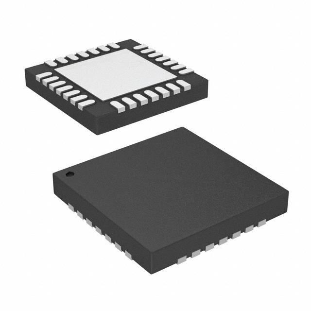
Small package: QFN28 (4 mm × 4 mm × 0.8 mm, 0.4 mm pitch)
*: DD1,DD2 : DC/DC converter block 1, 2
Applications
Network equipment: Wifi-tuner, Surveillance camera
Data-storage device: HDD, SSD, Picture recording equipment
Image and voice output equipment: MFP, Printer, Scanner, Projector, Electrophone, STB
Various terminals: POS, FA, HEMS
etc.
Cypress Semiconductor Corporation
Document Number: 002-08407 Rev. *D
•
198 Champion Court
•
San Jose, CA 95134-1709
•
408-943-2600
Revised February 16, 2022
�CY39C031
Contents
Description .......................................................................................................................................................... 1
Features ............................................................................................................................................................. 1
Applications ........................................................................................................................................................ 1
1. Application Circuit Example......................................................................................................................... 3
2. Recommended Application Specifications .................................................................................................. 4
3. Pin Assignment ............................................................................................................................................ 6
4. Pin Descriptions (PKG) ............................................................................................................................... 7
5. Block Diagram ............................................................................................................................................. 9
6. Absolute Maximum Ratings....................................................................................................................... 10
7. Recommended Operating Conditions ........................................................................................................11
8. Electrical Characteristics ........................................................................................................................... 12
9. Operation Mode List .................................................................................................................................. 15
10. State Transition Diagram ........................................................................................................................... 16
11. Turning On and Off Sequence (Turning On CTL*:CTL1, CTL2, CTLMAIN=VCC Simultaneously) .......... 17
12. CTL* Turning On and Off Sequence 1 (VCC→CTL*: CTL1, CTL2, CTLMAIN) ........................................ 18
13. CTL* Turning On and Off Sequence 2(VCC→CTLMAIN→CTL1→CTL2) ................................................ 19
14. CTL* Pin Threshold Voltage ...................................................................................................................... 20
15. Protection Operation Sequence ................................................................................................................ 21
16. Operation Condition, Stop Circuit and Release Condition for Protection Circuit ...................................... 23
17. DD Soft-Start Operation ............................................................................................................................ 24
18. Discharge Operation ................................................................................................................................. 25
19. PG1/PG2/PGL PIN and ERR PIN ............................................................................................................. 26
20. I2C Interface............................................................................................................................................... 27
21. Structure of I2C Interface and Data ........................................................................................................... 33
22. I/O Pin Equivalent Circuit Diagram ............................................................................................................ 38
23. I/O Circuit Type .......................................................................................................................................... 39
24. Typical Operation Characteristic Measurement Circuit ............................................................................. 40
25. Reference Data ......................................................................................................................................... 42
26. Usage Precaution ...................................................................................................................................... 62
27. Ordering Information ................................................................................................................................. 63
28. Preset Code (CY39C031) ......................................................................................................................... 63
29. Package Dimensions ................................................................................................................................. 64
Document History ............................................................................................................................................. 65
Sales, Solutions, and Legal Information ........................................................................................................... 66
Document Number: 002-08407 Rev. *D
Page 2 of 66
�CY39C031
1. Application Circuit Example
Vin
5.0V
MB39C031
4.7μF
4.7μF
0.1μF
LX1
IN1
PGND1
VCC
VCC
LX2
IN2
PGND2
4.7μF
CTL1
CTL2
CTLL
CTLMAIN
LDO
0.1μF
VR
VREF
Vo1
1.2V 1.4A
10μF
Vo2
1.8V 0.6A
10μF
LDO
3.3V 0.25A
10μF
VCCI2C
SCL
SDA
ADDSEL
I2C Signal
1.5μH
1.5μH
0.1μF
CTL Signal
0.47μF
PVCC1
PVCC2
PVCCL
100k 100k 100k 100k
PG1
PG2
PGL
ERR
GND
GND
Document Number: 002-08407 Rev. *D
Page 3 of 66
�CY39C031
2. Recommended Application Specifications
[Input Voltage Range]
Input Voltage VCC (V)
Min
Typ
Max
2.5
3.6
5.5
[Output Specification]
Accuracy
Symbol
Channel
(Ta=+25°C)
Output Limit
Output Voltage
Current Current
(V)
(mA) (mA)
Min Typ Max
Max
Min
14.3
1.01 1.02 1.03
0.9*
1.03 1.04 1.05
1.8
1.05 1.06 1.07
2.7
1.07 1.08 1.09
3.6
1.09* 1.10* 1.11*
4.5
1.13 1.14 1.15
1.15 1.16 1.17
5.4
Buck
1400
1.17 1.18 1.19
2000 (synchronous
rectification)
C-mode
3.0
1.5
10
6.3
7.2
9.0
1.21 1.22 1.23
9.9
1.23 1.24 1.25
10.8
1.24 1.26 1.28
11.6
1.26 1.28 1.30
12.5
1.28* 1.30* 1.32*
13.4
1.19* 1.20* 1.21*
14.3
1.24 1.25 1.27
0.9*
1.28 1.30 1.32
1.8
1.33* 1.35* 1.37*
2.7
1.38 1.40 1.42
3.6
1.43 1.45 1.47
4.5
1.53 1.55 1.57
1.58 1.60 1.62
5.4
Buck
600
1.63 1.65 1.67
900
(synchronous
rectification)
C-mode
3.0
1.5
10
6.3
7.2
8.1
1.68 1.70 1.72
9.0
1.73 1.75 1.77
9.9
1.78* 1.80* 1.82*
10.8
1.83 1.85 1.87
11.6
1.88 1.90 1.92
12.5
1.93 1.95 1.97
13.4
Document Number: 002-08407 Rev. *D
5
8.1
1.19* 1.20* 1.21*
1.48* 1.50* 1.52*
DD2 Vo2 ±1.2%
Switching Coil
Output
Soft-start Discharge
Capacitance Time Resistance Remarks
Frequency
(μH)
(ms)
(MHz)
(μF)
(kΩ)
0.99* 1.00* 1.01*
1.11 1.12 1.13
DD1 Vo1 ±1.2%
Mode
5
Built-in SW
FET
Built-in
output
setting
resistors
Operation
mode
switching
(Fixed
PWM,
PFM/PWM)
Built-in SW
FET
Built-in
output
setting
resistors
Operation
mode
switching
(Fixed
PWM,
PFM/PWM)
Page 4 of 66
�Accuracy
Symbol
Channel
CY39C031
LDO LDO ±1.8%
Output Limit
Output Voltage
Current Current
(V)
(mA) (mA)
Min Typ Max
Max
Mode
Min
Switching Coil
Output
Soft-start Discharge
Capacitance Time Resistance Remarks
Frequency
(μH)
(ms)
(MHz)
(μF)
(kΩ)
2.75 2.80 2.85
14.3
2.80* 2.85* 2.90*
0.9
2.95 3.00 3.05
1.8
3.24* 3.30* 3.36*
2.7*
-
-
-
3.6
-
-
-
4.5
-
-
-
5.4
-
-
-
-
-
-
-
-
-
8.1
-
-
-
9.0
-
-
-
9.9
-
-
-
10.8
-
-
-
11.6
-
-
-
12.5
-
-
-
13.4
250
300
LDO
-
-
4.7
6.3
7.2
5
*: Preset value
Note: It is possible to set the output voltage and to change the soft-start time using I2C.
Document Number: 002-08407 Rev. *D
Page 5 of 66
�CY39C031
3. Pin Assignment
VCC
ERR
PVCCL
LDO
PGL
CTLL
GND
(TOP VIEW)
28
27
26
25
24
23
22
CTL1
1
21
CTL2
PG1
2
20
PG2
PGND1
3
19
PGND2
LX1
4
18
LX2
PVCC1
5
17
PVCC2
IN1
6
16
IN2
CTLMAIN
7
15
VREF
Top View
8
9
10
11
12
13
14
VCC
VCCI2C
SCL
SDA
ADDSEL
GND
VR
EP(Exposed Pad)
(WNO028)
Document Number: 002-08407 Rev. *D
Page 6 of 66
�CY39C031
4. Pin Descriptions (PKG)
Circuit
Block
DD1
DD2
LDO
CTL
ERR
Numb
er of Pin
Pin Name
pin for No
PKG
I/O
Description
(PKG)
PullPAD
down Treatment
Resist when not
ance using DD1
PAD
Treatment
when not
using DD2
PAD
Treatment
PAD
when not
Treatment
using I2C
when not
using LDO Communicati
on
IN1
1
6
I
DD1·Output
voltage feedback
pin.
-
GND
connection
-
-
-
PVCC1
1
5
-
DD1·Output block
power supply pin
-
VCC
connection
-
-
-
LX1
1
4
O
DD1·Pin for
inductance
connection.
-
Open
-
-
-
PG1
1
2
O
DD1·POWERGOO
D output pin
-
Open
-
-
-
PGND1
1
3
-
DD1·Output block
ground pin
-
GND
connection
-
-
-
IN2
1
16
I
DD2·Output
voltage feedback
pin.
-
-
GND
connection
-
-
PVCC2
1
17
-
DD2·Output block
power supply pin
-
-
VCC
connection
-
-
LX2
1
18
O
DD2·Pin for
inductance
connection.
-
-
Open
-
-
PG2
1
20
O
DD2·POWERGOO
D output pin
-
-
Open
-
-
PGND2
1
19
-
DD2·Output block
ground pin
-
-
GND
connection
-
-
PVCCL
1
26
-
LDO·Power supply
pin
-
-
-
VCC
connection
-
LDO
1
25
O
LDO·Output pin
-
-
-
Open
-
PGL
1
24
O
LDO·POWERGOO
D output pin
-
-
-
Open
-
CTL1
1
1
I
DD1 Control pin
CTL2
1
21
I
DD2 Control pin
-
CTLL
1
23
I
LDO Control pin
-
-
CTLMAIN
1
7
I
Control pin for
common block and
digital block *
-
-
-
-
ERR
1
27
O
ERR signal output
pin
-
-
-
-
-
Document Number: 002-08407 Rev. *D
Open
Open
-
-
-
-
Open
-
Page 7 of 66
�CY39C031
Circuit
Block
Numb
er of Pin
Pin Name
pin for No
PKG
I/O
Description
(PKG)
PullPAD
down Treatment
Resist when not
ance using DD1
PAD
Treatment
when not
using DD2
PAD
Treatment
PAD
when not
Treatment
using I2C
when not
using LDO Communicati
on
VCCI2C
1
9
-
Power supply pin
for I2C.
-
-
-
-
GND
connection
SCL
1
10
I
I2C clock pin
×
-
-
-
Open
SDA
1
11
I/O
I2C data I/O pin
×
-
-
-
Open
ADDSEL
1
12
I
Switch pin for slave
address
-
-
-
Open
VCC
2
8,
28
-
Control circuit block
power supply pin
-
-
-
-
-
VREF
1
15
O
Reference voltage
(2.4 V) output pin
-
-
-
-
-
VR
1
14
O
Reference voltage
(0.6 V) output pin
-
-
-
-
-
GND
2
13,
22
-
Control circuit block
ground pin
-
-
-
-
-
GND
1
EP
-
Ground pin
-
-
-
-
-
I2C
Commo
n
-
*: When turning on DD1, DD2 and LDO, it is also necessary to set CTLMAIN to "H". See 9. Operation Mode List for the details.
Document Number: 002-08407 Rev. *D
Page 8 of 66
�CY39C031
5. Block Diagram
IN1
PVCC1
VCC:2.5V to 5.5V
L Priority
A
VCC
VCC
VCC
ErrAMP
ctl1
PWM
Logic AST
Control
ICOMP
LX1
Vo1:1.00V to 1.30V
(20mV step)
Io(Max):1400mA
0.6V
DEC
UVLO
POR
A
LV
CNV
PGND1
SLP
PG1
IN2
scp1
cs1
vsel1
clk1
PVCC2
L Priority
B
VCC
VCC
PWM
Logic AST
Control
ICOMP
LX2
Vo2:1.20V to 1.95V
(50mV step)
Io(Max):600mA
0.6V
DEC
UVLO
POR
B
VCC
ErrAMP
ctl2
LV
CNV
PGND2
SLP
PG2
cs2
vsel2
scp2
clk2
PVCCL
LDO:2.80V/2.85V/
3.00V/3.30V
Io(Max):250mA
LDO
0.6V
ctll
DEC
UVLO
POR
csl
vsell
PGL
scpl
VREF
CTLMAIN
Logic control
block
ctlmain
VCCI2C
SCL
SDA
ADDSEL
CTL1
ctl1
CTL2
ctl2
CTLL
ctll
scp1/2/l
ERR
SCP (counter & latch)
OTP
Soft-start control
Output voltage
switch control
Common block
power supply
ctlmain
cs1/2/l
Common block
vsel1/2/l
VR,OSC,logic power supply
VREF
VCC
VCC
BGR
UVLO
VREF
VREF
Reference
0.6V
OSC
CT
RT
VR
clk1/2
VREF
(2.4V)
Document Number: 002-08407 Rev. *D
VR
GND
GND
: Pin
(0.6V)
Page 9 of 66
�CY39C031
6. Absolute Maximum Ratings
Parameter
Power supply voltage
Input voltage
LX voltage
Symbol
Condition
Rating
Min
Max
Unit
VCC
VCC, PVCC1, PVCC2, PVCCL,
VCCI2C pins
-
7
V
VCTL
CTLMAIN, 1, 2, L pins
-
7
V
VOUT
IN1, IN2 pins
-
7
V
Vlogic
SDA, SCL pins
-
7
V
VLX
LX1, LX2 pins
-0.3
+7
V
-
1720
mW
Ta ≤ +25°C
Power dissipation
PD
Maximum junction temperature
Tjmax
-
-
+125
°C
Storage temperature
TSTG
-
-55
+125
°C
Thermal resistor value
(θj-a):(50°C/W*)
*: When mounted on a QFN28 (WNO028) PKG, 4layers 0.8 mm thickness 117 mm × 84 mm
WARNING: Semiconductor devices can be permanently damaged by application of stress (voltage, current, temperature, etc.)
in excess of absolute maximum ratings. Do not exceed these ratings.
Document Number: 002-08407 Rev. *D
Page 10 of 66
�CY39C031
7. Recommended Operating Conditions
Parameter
Power supply
voltage
General
Reference
voltage
output
current
Symbol
Condition
Max
Unit
VCC pin
2.5
3.6
5.5
V
IREF
VREF pin
-1
-
0
mA
IR
VR pin
-1
-
0
μA
-30
+25
+85
°C
2.5
3.6
5.5
V
0
-
VCC
V
3.5
3.6
5.5
V
0
-
VCC
V
1.76
-
3.37
V
0
-
VCCI2C
V
Ta
Power supply
voltage
VCC
VCC, PVCC1, PVCC2 pins
Input voltage
VOUT
IN1, IN2 pins
LDO CH
Power supply
voltage
VCC
CTL
block
Input voltage
VCTL
CTL* pin
Power supply
voltage
VCC
VCCI2C pin
Logic
input voltage
Vlogic
SDA, SCL pin
Digital
block
(I2C)
Typ
VCC
Operating
temperature
DC/DC
CH
Value
Min
-
VCC, PVCCL pins
Output voltage setting: default (3.3 V)
*: CTLMAIN, CTL1, CTL2, CTLL
WARNING: The recommended operating conditions are required in order to ensure the normal operation of the semiconductor
device. All of the device's electrical characteristics are warranted when the device is operated within these ranges.
Always use semiconductor devices within their recommended operating condition ranges. Operation outside these
ranges may adversely affect reliability and could result in device failure.
No warranty is made with respect to uses, operating conditions, or combinations not represented on the data sheet.
Users considering application outside the listed conditions are advised to contact their representatives beforehand.
Document Number: 002-08407 Rev. *D
Page 11 of 66
�CY39C031
8. Electrical Characteristics
Common Block
(Ta=+25°C, VCC=PVCC1, PVCC2, L=3.6V)
Parameter
Symbol
Condition
Value
Min
Typ
Max
Unit
VR
VR pin =0 mA
0.594
0.600
0.606
V
VREF1
VREF pin =0 mA
2.376
2.400
2.424
V
VREF2
VCC pin =2.5 V to 5.5 V
2.370
2.400
2.430
V
VREF3
VREF pin =0 mA to -1 mA
2.370
2.400
2.430
V
Threshold voltage
VTH
VCC pin =
2.156
2.20
2.244
V
Hysteresis width
VH
-
0.20
-
V
Over Current
Protection Circuit
Block [OCP]
Timer time
tOCP1
0.5
1
1.5
ms
Thermal shutdown
Protection Circuit
Block [TSD]
Stop temperature
TTSDH
-
150*
-
°C
VCC
× 0.7
-
VCC
V
Reference Voltage
Block
[VR, VREF]
Under Voltage
Lockout Protection
Circuit Block
[VCC UVLO]
Output voltage
Input voltage
Control Block
(CTL)
[CTL]
Input current
Input pull-down resistor
General
(DC/DC block)
Power supply current
DD1, DD2, LDO Default value
-
VIH
CTL* pin
VIL
CTL* pin
ICTLH
CTL* pin =3.6 V
ICTLL
0
-
0.4
V
2.7
3.6
5.1
μA
CTL* pin =0 V
-
-
1
μA
RP
CTL* pin
-
1
-
MΩ
IVCCS1
CTL* pin =0 V
-
0
1.0
μA
IVCCS2
CTLMAIN=3.6 V
CTL1, CTL2.L pins =0 V
-
80
120
μA
IVCC
CTLMAIN, L pins =3.6 V Only LDO
operation No load
-
200
300
μA
IVCC
CTL* pin = 3.6 V
all CH No load
(DD operation mode: PFM/PWM
mode)
-
450
680
μA
-
10.8
16.2
mA
-
7.2
12.0
μA
IVCC
IVCCI2C
CTL* pin = 3.6 V
all CH No load
(DD operation mode:
Fixed PWM mode)
CTLMAIN, L pin=3.6 V
VCCI2C pin = 1.8 V
*: These are not the rated values. Use these values as reference when planning.
Document Number: 002-08407 Rev. *D
Page 12 of 66
�CY39C031
DD1, DD2
(Ta=+25°C, VCC=PVCC1, PVCC2, L=3.6V)
Parameter
Symbol
Output voltage
VOUT
Input stability
VLINE
Load stability
VLOAD
Condition
Output voltage setting: 1.2 V
IOUT=-10 mA
Value
Unit
Min
Typ
Max
1.186
1.20
1.214
V
IOUT=-10 mA, VCC=2.5 V to 5.5 V
-5
-
+5
mV
IOUT=-1 mA to -1400 mA (when in
Fixed PWM mode)
-10
-
-
mV
IOUT=-1 mA to -1400 mA (when in
PFM/PWM mode)
-10
-
+15
mV
IN1 pin=1.5 V
DC/DC
Converter Block
[DD1]
IN1 pin input impedance
RIN
output voltage setting:
1.2 V
-
400
-
kΩ
SW PMOS-Tr ON
resistance
RPMOS
LX1 pin=-30 mA
-
0.12*
-
Ω
SW NMOS-Tr ON
resistance
RNMOS
LX1 pin= 30 mA
-
0.09*
-
Ω
SW PMOS-Tr leak current
ILEAK
LX1 pin=0 V
-1
-
-
μA
SW NMOS-Tr leak current
ILEAK
LX1 pin=3.6 V
-
-
1
μA
Overcurrent protection
value
ILIMIT
L=1.5 μH
2000
-
-
mA
PFM/PWM reshuffling
electric current
IPFM
L=1.5 μH
-
40*
-
mA
Discharge resistor
RDIS
-
-
5
-
kΩ
Soft-start time
tSS
0.8
0.9
1.0
ms
Switching frequency
fOSC
-
2.7
3.0
3.3
MHz
Output voltage
VOUT
Output voltage setting: 1.8 V
IOUT=-10 mA
1.778
1.80
1.822
V
Input stability
VLINE
IOUT=-10mA VCC=2.5 V to 5.5 V
-5
-
+5
mV
IOUT=-1 mA to -600mA (when in
Fixed PWM mode)
-10
-
-
mV
IOUT=-1 mA to -600mA (when in
PFM/PWM mode)
-10
-
+20
mV
Load stability
DC/DC
Converter Block
[DD2]
VLOAD
Preset value
IN2 pin input impedance
RIN
IN2 pin =2.0 V
Output voltage setting: 1.8 V
-
300
-
kΩ
SW PMOS-Tr ON
resistance
RPMOS
LX2 pin =-30 mA
-
0.16*
-
Ω
SW NMOS-Tr ON
resistance
RNMOS
LX2 pin = 30 mA
-
0.14*
-
Ω
SW PMOS-Tr leak current
ILEAK
LX2 pin =0 V
-1
-
-
μA
SW NMOS-Tr leak current
ILEAK
LX2 pin =3.6 V
-
-
1
μA
Overcurrent protection
value
ILIMIT
L=1.5 μH
900
-
-
mA
PFM/PWM reshuffling
electric current
IPFM
L=1.5 μH
-
70*
-
mA
Discharge resistor
RDIS
Soft-start time
tSS
Switching frequency
fOSC
Preset value
-
-
5
-
kΩ
0.8
0.9
1.0
ms
2.7
3.0
3.3
MHz
*: These are not the rated values. Use these values as reference when planning.
Document Number: 002-08407 Rev. *D
Page 13 of 66
�CY39C031
LDO
(Ta=+25°C, VCC=PVCC1, PVCC2, L=3.6V)
Parameter
LDO Block
[LDO]
Symbol
Output voltage
VOUT
I/O voltage difference
VDIF
Input stability
VLINE
Load stability
VLOAD
Ripple remove ratio
RR
Value
Condition
Unit
Min
Typ
Max
3.241
3.300
3.359
V
-
-
0.20
V
-5
-
+5
mV
IOUT=-1mA to -150 mA
-30
-20
-
mV
PVCCL=0.2 Vrms, f=10 Hz,
IOUT=-150 mA
35
75
-
dB
15
50
-
dB
Output voltage setting : 3.3 V
IOUT=-10 mA
IOUT=-10 mA
IOUT=-10 mA,
VCC=3.5 V to 5.5 V
PVCCL=0.2 Vrms, f=10 kHz,
IOUT=-150 mA
Overcurrent protection value
ILIMIT
Vout×0.9
Control macro consumption
current
IPVCCLS
At stand-by
IPVCCL
IOUT=0 mA
Discharge resistor
RDIS
Soft-start time
tSS
300
-
-
mA
-
0
1
μA
-
80
105
μA
-
5
-
kΩ
2.4
2.7
3.0
ms
Preset value
Digital Block
(Ta=+25°C, VCC=PVCC1, PVCC2, L=3.6V)
Parameter
Symbol
Condition
Value
Min
Typ
Max
Unit
Output voltage
VOL
PG1, PG2, L pins IOL=1mA
-
-
0.4
V
Output current
IOL
PG1, PG2, L pins
1
-
-
mA
Low-voltage detection
Vth
IN1, IN2, LDO pins =
-
Vo ×
0.75*
-
V
Power-on detection voltage
Vth
IN1, IN2, LDO pins =
-
Vo ×
0.85*
-
V
Error Block
Output voltage
VOL
ERR pin IOL = 1 mA
-
-
0.4
V
[ERR]
Output current
IOL
ERR pin
1
-
-
mA
VIH
SCL, SDA pins VCCI2C=3.3 V
VCCI2C
× 0.7
-
VCCI2C
V
VIL
SCL, SDA pins VCCI2C=3.3 V
0
-
VCCI2C
× 0.3
V
IIH
SCL, SDA pins VCCI2C=3.3 V
-
-
10
μA
POWER-GOOD
Block
[Power Good ]
Input voltage
2
I C Block
[I2C]
Input current
IIL
SCL, SDA pins VCCI2C=3.3 V
-10
-
-
μA
Output voltage
VOL
SDA pin IOL =3 mA
-
-
0.4
V
Output current
IOL
SDA pin
3
-
-
mA
Input pull-down resistor
RP
ADDSEL pin
-
1
-
MΩ
*: These are not the rated values. Use these values as reference when planning.
Document Number: 002-08407 Rev. *D
Page 14 of 66
�CY39C031
9. Operation Mode List
Mode
CTL Signal
Operation Block
I2C
Communication
Protection
Operating
Stand-by
Stand-by 2
CTLMAIN (External)
L
CTL1 (External / I2C)
L
CTL2 (External / I C)
CTLL (External / I2C)
2
General
ERR detection
H
H
H
L
H/L
X
L
L
H/L
X
L
L
H/L
X
General
OFF
ON
ON
ON
Digital Block
OFF
ON
ON
ON
OSC, VR Block
OFF
OFF
ON*2
OFF
DD1
OFF
OFF
ON/OFF
OFF
DD2
OFF
OFF
ON/OFF
OFF
LDO
OFF
OFF
ON/OFF
OFF
I2C communication
Disabled
Enabled
Enabled
Enabled
Thermal shutdown
Protection (TSD)
Not available
Not available
Available
*1
Over Current Protection
(OCP)
Not available
Not available
Available
*1
*1:This is the state after detection of ERR. It is possible to release the ERR detection mode by turning the power
supply on again or turning CTLMAIN on again.
*2:When only LDO is operating, the OSC block stops (OFF) after LDO activation. Also, the VR block keeps
operating (ON) after LDO activation.
Priority of the external pin/I2C communication for CTL1, CTL2 and L
CTLMAIN
(External Pin)
CTL*
(External Pin)
CTL*
(I2C Communication)
Relevant CH
H
H
H
Unavailable
H
H
L
ON
H
L
H
ON
H
L
L
OFF
L
X
Communication disabled
OFF
*:The I2C communication is enabled after the common block and digital block activation setting the external CTLMAIN pin to "H".
When executing the ON/OFF control for DD1, DD2 and LDO using the external pin, don't execute the
ON/OFF control using I2C. Aside from the ON/OFF control, it is possible to control everything else using I2C.
When executing the ON/OFF control for DD1, DD2 and LDO using I2C, input "L" to the CTL* pin (the pin
connection condition).
Document Number: 002-08407 Rev. *D
is open or in the GND
Page 15 of 66
�CY39C031
10.
State Transition Diagram
Stand-by
(1)
(2)
Stand-by 2
(3)
(4)
General
(5)
(6)
Error
detection
(1)External CTLMAIN pin "H"
(2)External CTLMAIN pin "L"
(3)External CTL pin "H" / I2C communication "relevant CH_ON"
(4)External CTL pin "L" / I2C communication "relevant CH_OFF"
(5)Error detection (OCP, OCP_1ms continuation)
(6)Turning on the power supply again (equal to or less than uvlo_vcc reset voltage) or setting CTLMAIN to "L"
Notes:
When executing the ON/OFF control for DD1, DD2 and LDO using the external pin, don't execute the
I2C. Aside from the ON/OFF control, it is possible to control everything else using I2C.
ON/OFF control using
When executing the ON/OFF control for DD1, DD2 and LDO using I2C, input "L" to the CTL* pin (the pin is open or in the GND
connection condition).
Document Number: 002-08407 Rev. *D
Page 16 of 66
�CY39C031
11. Turning On and Off Sequence (Turning On CTL*:CTL1, CTL2, CTLMAIN=VCC
Simultaneously)
2.0V
2.2V
VCC
VCCI2C
0V
CTL*
uvlo_vcc
(IC internal signal)
2.4V
VREF
90%
VR
0.6V
osc
(IC internal signal)
ctl*
(IC internal signal)
85%
Discharge
85%
Discharge
DD1
PG1
DD2
PG2
UVLO release to DD*activation
Time till start *
Typ:200μS
Max:300μS
Soft-start time
*: VREF and VR activations depend on the VREF pin capacitance and VR pin capacitance.
Time in the sequence figure above is applied for the following condition.
VREF pin capacitance : 0.1 μF
VR pin capacitance : 0.47 μF
Document Number: 002-08407 Rev. *D
Page 17 of 66
�CY39C031
12.
CTL* Turning On and Off Sequence 1 (VCC→CTL*: CTL1, CTL2, CTLMAIN)
VCC
3.6V
VCCI2C
0V
CTL*
uvlo_vcc
(IC internal signal)
2.4V
VREF
VR
osc
(IC internal signal)
90%
0.6V
ctl*
(IC internal signal)
85%
Discharge
85%
Discharge
DD1
PG1
DD2
PG2
Turning on CTL * to DD*
activation
Time till start *
Typ:270μS
Max:450μS
Soft-start time
*: VREF and VR activations depend on the VREF pin capacitance and VR pin capacitance.
Time in the sequence figure above is applied for the following condition.
VREF pin capacitance : 0.1 μF
VR pin capacitance : 0.47 μF
Document Number: 002-08407 Rev. *D
Page 18 of 66
�CY39C031
13.
CTL* Turning On and Off Sequence 2(VCC→CTLMAIN→CTL1→CTL2)
VCC
3.6V
VCCI2C
0V
CTLMAIN
uvlo_vcc
(IC internal signal)
VREF
2.4V
(1)
CTL1
90%
VR
0.6V
osc (IC internal signal)
ctl1 (IC internal signal)
(2)
Discharge
85%
DD1
PG1
Soft-start time
CTL2
ctl2 (IC internal signal)
85%
DD2
Discharge
PG2
Soft-start time
(1)
Time from turning on CTLMAIN to VREF activation completion (=communication enabled)*
Typ: 130 μs, Max: 200 μs
(2)
Time from turning on CTL1 to ctll (IC internal signal) "H"
Typ: 150 μs, Max: 250 μs
*: VREF and VR activations depend on the VREF pin capacitance and VR pin capacitance.
Time in the sequence figure above is applied for the following condition.
VREF pin capacitance : 0.1 μF
VR pin capacitance : 0.47 μF
Document Number: 002-08407 Rev. *D
Page 19 of 66
�CY39C031
14.
CTL* Pin Threshold Voltage
The input circuit structure for the CTL* pin is the schmitt trigger style, and the threshold voltage shows the hysteresis
characteristics when CTL* OFF → ON and ON → OFF. (See "·CTL* pin equivalent circuit diagram" below.)
Also, the threshold voltage level depends on the VCC pin voltage.
Moreover, make sure to input either the "H" level (>"VCC×0.7"V) or "L" level (


 工商网监
湘ICP备2023018690号
工商网监
湘ICP备2023018690号
