CY62148E MoBL®
4-Mbit (512K × 8) Static RAM
4-Mbit (512K × 8) Static RAM
Features
advanced circuit design to provide ultra low standby current. This
is ideal for providing More Battery Life™ (MoBL) in portable
applications. The device also has an automatic power-down
feature that significantly reduces power consumption when
addresses are not toggling. Placing the device into standby
mode reduces power consumption by more than 99% when
deselected (CE HIGH). The eight input and output pins (I/O0
through I/O7) are placed in a high impedance state when the
device is deselected (CE HIGH), Outputs are disabled (OE
HIGH), or during an active Write operation (CE LOW and WE
LOW).
■
Very high speed: 45 ns
■
Voltage range: 4.5 V to 5.5 V
■
Pin compatible with CY62148B
■
Ultra low standby power
❐ Typical standby current: 1 µA
❐ Maximum standby current: 7 µA (Industrial)
■
Ultra low active power
❐ Typical active current: 2.0 mA at f = 1 MHz
■
Easy memory expansion with CE, and OE features
■
Automatic power-down when deselected
■
Complementary metal oxide semiconductor (CMOS) for
optimum speed and power
■
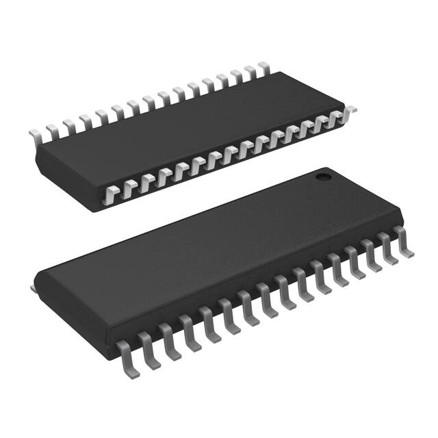
Available in Pb-free 32-pin thin small outline package (TSOP) II
and 32-pin small-outline integrated circuit (SOIC)[1] packages
To write to the device, take Chip Enable (CE) and Write Enable
(WE) inputs LOW. Data on the eight I/O pins (I/O0 through I/O7)
is then written into the location specified on the address pins (A0
through A18).
Functional Description
The CY62148E is a high performance CMOS static RAM
organized as 512K words by 8-bits. This device features
To read from the device, take Chip Enable (CE) and Output
Enable (OE) LOW while forcing Write Enable (WE) HIGH. Under
these conditions, the contents of the memory location specified
by the address pins appear on the I/O pins.
The CY62148E device is suitable for interfacing with processors
that have TTL I/P levels. It is not suitable for processors that
require CMOS I/P levels. Please see Electrical Characteristics
on page 4 for more details and suggested alternatives.
For a complete list of related documentation, click here.
Logic Block Diagram
I/O00
IO
INPUT BUFFER
I/O1
IO
1
I/O2
IO
2
SENSE AMPS
ROW DECODER
512K x 8
ARRAY
I/O3
IO
3
I/O4
IO
4
I/O5
IO
5
I/O6
IO
6
CE
I/O
IO77
POWER
DOWN
A17
A18
A13
A14
OE
A15
COLUMN DECODER
WE
A16
A0
A1
A2
A3
A4
A5
A6
A7
A8
A9
A10
A11
A12
Note
1. SOIC package is available only in 55 ns speed bin.
Cypress Semiconductor Corporation
Document Number: 38-05442 Rev. *P
•
198 Champion Court
•
San Jose, CA 95134-1709
•
408-943-2600
Revised June 1, 2016
�CY62148E MoBL®
Contents
Pin Configurations ........................................................... 3
Product Portfolio .............................................................. 3
Maximum Ratings ............................................................. 4
Operating Range ............................................................... 4
Electrical Characteristics ................................................. 4
Capacitance ...................................................................... 5
Thermal Resistance .......................................................... 5
AC Test Loads and Waveforms ....................................... 5
Data Retention Characteristics ....................................... 6
Data Retention Waveform ................................................ 6
Switching Characteristics ................................................ 7
Switching Waveforms ...................................................... 8
Truth Table ...................................................................... 10
Document Number: 38-05442 Rev. *P
Ordering Information ...................................................... 11
Ordering Code Definitions ......................................... 11
Package Diagrams .......................................................... 12
Acronyms ........................................................................ 14
Document Conventions ................................................. 14
Units of Measure ....................................................... 14
Document History Page ................................................. 15
Sales, Solutions, and Legal Information ...................... 18
Worldwide Sales and Design Support ....................... 18
Products .................................................................... 18
PSoC®Solutions ....................................................... 18
Cypress Developer Community ................................. 18
Technical Support ..................................................... 18
Page 2 of 18
�CY62148E MoBL®
Pin Configurations
Figure 1. 32-pin SOIC/TSOP II pinout
Top View
A17
A16
A14
A12
A7
A6
A5
A4
A3
A2
A1
A0
I/O0
I/O1
I/O2
VSS
1
2
3
4
5
6
7
8
9
10
11
12
13
14
15
16
32
31
30
29
28
27
26
25
24
23
22
21
20
19
18
17
VCC
A15
A18
WE
A13
A8
A9
A11
OE
A10
CE
I/O7
I/O6
I/O5
I/O4
I/O3
Product Portfolio
Power Dissipation
VCC Range (V)
Product
CY62148ELL
TSOP II
CY62148ELL
SOIC
Range
Min
Typ [2]
Max
Industrial
4.5
5.0
5.5
Industrial /
Automotive-A
4.5
5.0
5.5
Speed
(ns)
Operating ICC (mA)
f = 1 MHz
f = fmax
Standby ISB2 (µA)
Typ [2]
Max
Typ [2]
Max
Typ [2]
Max
45
2
2.5
15
20
1
7
55
2
2.5
15
20
1
7
Note
2. Typical values are included for reference only and are not guaranteed or tested. Typical values are measured at VCC = VCC(typ), TA = 25 °C.
Document Number: 38-05442 Rev. *P
Page 3 of 18
�CY62148E MoBL®
Maximum Ratings
Output current into outputs (LOW) ............................. 20 mA
Exceeding maximum ratings may shorten the useful life of the
device. User guidelines are not tested.
Storage temperature ............................... –65 °C to + 150 °C
Ambient temperature
with power applied .................................. –55 °C to + 125 °C
Static discharge voltage
(per MIL-STD-883, Method 3015) .......................... > 2001 V
Latch-up current .................................................... > 200 mA
Operating Range
Supply voltage
to ground potential ............. –0.5 V to 6.0 V (VCCmax + 0.5 V)
DC voltage applied to outputs
in high Z state [3, 4] ............. –0.5 V to 6.0 V (VCCmax + 0.5 V)
DC input voltage
[3, 4]
Device
Ambient
Temperature
Range
CY62148E
......... –0.5 V to 6.0 V (VCCmax + 0.5 V)
VCC[5]
Industrial / –40 °C to +85 °C 4.5 V to 5.5 V
Automotive-A
Electrical Characteristics
Over the operating range
Parameter
VOH[8]
Description
Output HIGH voltage
Test Conditions
VCC = 4.5 V, IOH = –1 mA
VCC = 5.5 V, IOH = –0.1 mA
55 ns [6]
45 ns
Min Typ
2.4
–
[7]
–
–
Max
–
3.4
2.4
[8]
VOL
Output LOW voltage
IOL = 2.1 mA
–
–
VIH
Input HIGH voltage
VCC = 4.5 V to 5.5 V
2.2
–
VIL
Input LOW voltage
VCC = 4.5 V to 5.5 V For TSOPII
package
–0.5
–
0.8
–
–
–
For SOIC
package
0.4
–
–
–
–
Max
–
3.4
Unit
V
[8]
V
–
0.4
V
–
VCC + 0.5
V
–
–
–
V
–0.5
–
0.6 [9]
VCC + 0.5 2.2
IIX
Input leakage current
–1
–
+1
–1
–
+1
µA
IOZ
Output leakage current GND < VO < VCC, output disabled
–1
–
+1
–1
–
+1
µA
ICC
VCC operating supply
current
f = fmax = 1/tRC
–
15
20
–
15
20
mA
–
2
2.5
–
2
2.5
Automatic CE
power-down current –
CMOS inputs
CE > VCC – 0.2 V,
VIN > VCC – 0.2 V or VIN < 0.2 V,
f = 0, VCC = VCC(max)
–
1
7
–
1
7
ISB2 [10]
GND < VI < VCC
Min Typ [7]
f = 1 MHz
VCC = VCC(max),
IOUT = 0 mA
CMOS levels
µA
Notes
3. VIL(min) = –2.0 V for pulse durations less than 20 ns for I < 30 mA.
4. VIH(max) = VCC + 0.75 V for pulse durations less than 20 ns.
5. Full device AC operation assumes a minimum of 100 µs ramp time from 0 to VCC(min) and 200 µs wait time after VCC stabilization.
6. SOIC package is available only in 55 ns speed bin.
7. Typical values are included for reference and are not guaranteed or tested. Typical values are measured at VCC = VCC(typ), TA = 25 °C.
8. Please note that the maximum VOH limit for this device does not exceed minimum CMOS VIH of 3.5V. If you are interfacing this SRAM with 5 V legacy processors
that require a minimum VIH of 3.5 V, please refer to Application Note AN6081 for technical details and options you may consider.
9. Under DC conditions the device meets a VIL of 0.8 V. However, in dynamic conditions Input LOW Voltage applied to the device must not be higher than 0.6 V. This
is applicable to SOIC package only.
10. Chip enable (CE) must be HIGH at CMOS level to meet the ISB2 / ICCDR spec. Other inputs can be left floating.
Document Number: 38-05442 Rev. *P
Page 4 of 18
�CY62148E MoBL®
Capacitance
Parameter [11]
Description
CIN
Input capacitance
COUT
Output capacitance
Test Conditions
TA = 25 °C, f = 1 MHz, VCC = VCC(Typ)
Max
Unit
10
pF
10
pF
Thermal Resistance
Parameter [11]
Test Conditions
32-pin SOIC
Package
Still air, soldered on a 3 × 4.5 inch,
four-layer printed circuit board
51.57
59.10
C/W
25.01
12.19
C/W
Description
JA
Thermal resistance
(junction to ambient)
JC
Thermal resistance
(junction to case)
32-pin TSOP II Unit
Package
AC Test Loads and Waveforms
Figure 2. AC Test Loads and Waveforms
R1
VCC
OUTPUT
ALL INPUT PULSES
3.0 V
30 pF
INCLUDING
JIG AND
SCOPE
10%
R2
90%
GND
Rise Time = 1 V/ns
Equivalent to:
90%
10%
Fall Time = 1 V/ns
THEVENIN EQUIVALENT
RTH
OUTPUT
VTH
Parameter [11]
5.0 V
Unit
R1
1800
R2
990
RTH
639
VTH
1.77
V
Note
11. Tested initially and after any design or process changes that may affect these parameters.
Document Number: 38-05442 Rev. *P
Page 5 of 18
�CY62148E MoBL®
Data Retention Characteristics
Over the operating range
Parameter
Description
VDR
VCC for data retention
ICCDR[13]
Data retention current
Conditions
VCC = VDR,
CE > VCC – 0.2 V,
VIN > VCC – 0.2 V or
VIN < 0.2 V
tCDR
Chip deselect to data retention
time
tR[14]
Operation recovery time
Industrial /
Automotive-A
Min
Typ [12]
Max
Unit
2
–
–
V
–
1
7
µA
0
–
–
ns
45/55
–
–
ns
Data Retention Waveform
Figure 3. Data Retention Waveform
DATA RETENTION MODE
VCC
VCC(min)
tCDR
VDR > 2.0 V
VCC(min)
tR
CE
Notes
12. Typical values are included for reference and are not guaranteed or tested. Typical values are measured at VCC = VCC(typ), TA = 25 °C.
13. Chip enable (CE) must be HIGH at CMOS level to meet the ISB2 / ICCDR spec. Other inputs can be left floating.
14. Full device operation requires linear VCC ramp from VDR to VCC(min) > 100 µs or stable at VCC(min) > 100 µs.
Document Number: 38-05442 Rev. *P
Page 6 of 18
�CY62148E MoBL®
Switching Characteristics
Over the operating range
Parameter [15, 16]
Description
55 ns [17]
45 ns
Min
Max
Min
Max
Unit
Read Cycle
tRC
Read cycle time
45
–
55
–
ns
tAA
Address to data valid
–
45
–
55
ns
tOHA
Data hold from address change
10
–
10
–
ns
tACE
CE LOW to data valid
–
45
–
55
ns
tDOE
OE LOW to data valid
–
22
–
25
ns
tLZOE
OE LOW to low Z [18]
5
–
5
–
ns
–
18
–
20
ns
10
–
10
–
ns
–
18
–
20
ns
tHZOE
tLZCE
OE HIGH to high Z
CE LOW to low Z
[18, 19]
[18]
[18, 19]
tHZCE
CE HIGH to high Z
tPU
CE LOW to power-up
0
–
0
–
ns
CE HIGH to power-down
–
45
–
55
ns
tPD
Write Cycle
[20, 21]
tWC
Write cycle time
45
–
55
–
ns
tSCE
35
–
40
–
ns
tAW
CE LOW to write end
Address setup to write end
35
–
40
–
ns
tHA
Address hold from write end
0
–
0
–
ns
tSA
Address setup to write start
0
–
0
–
ns
tPWE
35
–
40
–
ns
tSD
WE pulse width
Data setup to write end
25
–
25
–
ns
tHD
Data hold from write end
0
–
0
–
ns
–
18
–
20
ns
10
–
10
–
ns
[18, 19]
tHZWE
WE LOW to high Z
tLZWE
WE HIGH to low Z [18]
Notes
15. In an earlier revision of this device, under a specific application condition, READ and WRITE operations were limited to switching of the chip enable signal as described
in the Application Note AN66311. However, the issue has been fixed and in production now, and hence, this Application Notes is no longer applicable. It is available
for download on our website as it contains information on the date code of the parts, beyond which the fix has been in production.
16. Test conditions for all parameters other than tri-state parameters assume signal transition time of 3 ns or less, timing reference levels of 1.5 V, input pulse levels of
0 to 3 V, and output loading of the specified IOL/IOH as shown in the Figure 2 on page 5.
17. SOIC package is available only in 55 ns speed bin.
18. At any temperature and voltage condition, tHZCE is less than tLZCE, tHZOE is less than tLZOE, and tHZWE is less than tLZWE for any device.
19. tHZOE, tHZCE, and tHZWE transitions are measured when the outputs enter a high impedance state.
20. The internal wre.ite time of the memory is defined by the overlap of WE, CE = VIL. All signals must be ACTIVE to initiate a write and any of these signals can terminate
a write by going INACTIVE. The data input setup and hold timing should be referenced to the edge of the signal that terminates the write.
21. The minimum write cycle pulse width for Write Cycle No. 3 (WE Controlled, OE LOW) should be equal to the sum of tSD and tHZWE.
Document Number: 38-05442 Rev. *P
Page 7 of 18
�CY62148E MoBL®
Switching Waveforms
Figure 4. Read Cycle No. 1 (Address Transition Controlled) [22, 23]
tRC
RC
ADDRESS
tOHA
DATA OUT
tAA
PREVIOUS DATA VALID
DATA VALID
Figure 5. Read Cycle No. 2 (OE Controlled) [23, 24]
ADDRESS
tRC
CE
tACE
OE
tHZOE
tDOE
tHZCE
tLZOE
HIGH IMPEDANCE
DATA OUT
DATA VALID
tLZCE
tPD
tPU
VCC
SUPPLY
CURRENT
HIGH
IMPEDANCE
50%
50%
ICC
ISB
Figure 6. Write Cycle No. 1 (WE Controlled, OE HIGH During Write) [25, 26]
tWC
ADDRESS
tSCE
CE
tAW
tSA
tHA
tPWE
WE
OE
tSD
DATA I/O
NOTE 27
tHD
DATA VALID
tHZOE
Notes
22. Device is continuously selected. OE, CE = VIL.
23. WE is HIGH for read cycles.
24. Address valid before or similar to CE transition LOW.
25. Data I/O is high impedance if OE = VIH.
26. If CE goes HIGH simultaneously with WE HIGH, the output remains in high impedance state.
27. During this period, the I/Os are in output state and input signals must not be applied.
Document Number: 38-05442 Rev. *P
Page 8 of 18
�CY62148E MoBL®
Switching Waveforms (continued)
Figure 7. Write Cycle No. 2 (CE Controlled) [28, 29]
tWC
ADDRESS
tSCE
CE
tSA
tAW
tHA
tPWE
WE
tSD
DATA I/O
tHD
DATA VALID
Figure 8. Write Cycle No. 3 (WE Controlled, OE LOW) [29, 30]
tWC
ADDRESS
tSCE
CE
tAW
tSA
tHA
tPWE
WE
tSD
DATA I/O
NOTE 31
tHD
DATA VALID
tHZWE
tLZWE
Notes
28. Data I/O is high impedance if OE = VIH.
29. If CE goes HIGH simultaneously with WE HIGH, the output remains in high impedance state.
30. The minimum write cycle pulse width should be equal to the sum of tSD and tHZWE.
31. During this period, the I/Os are in output state and input signals must not be applied.
Document Number: 38-05442 Rev. *P
Page 9 of 18
�CY62148E MoBL®
Truth Table
CE
H
WE
OE
[32]
I/O
Mode
Power
X
X
High Z
Deselect/power-down
Standby (ISB)
L
H
L
Data out
Read
Active (ICC)
L
L
X
Data in
Write
Active (ICC)
L
H
H
High Z
Selected, outputs disabled
Active (ICC)
Note
32. Chip enable (CE) must be HIGH at CMOS level to meet the ISB2 / ICCDR spec. Other inputs can be left floating.
Document Number: 38-05442 Rev. *P
Page 10 of 18
�CY62148E MoBL®
Ordering Information
Table 1 lists the CY62148E MoBL® key package features and ordering codes. The table contains only the parts that are currently
available. If you do not see what you are looking for, contact your local sales representative. For more information, visit the Cypress
website at www.cypress.com and refer to the product summary page at http://www.cypress.com/products.
Table 1. Key features and Ordering Information
Speed
(ns)
45
55
Package
Diagram
Ordering Code
Package Type
Operating
Range
CY62148ELL-45ZSXI
51-85095 32-pin TSOP II (Pb-free)
Industrial
CY62148ELL-45ZSXA
51-85095 32-pin TSOP II (Pb-free)
Automotive-A
CY62148ELL-55SXI
51-85081 32-pin SOIC (Pb-free)
Industrial
CY62148ELL-55SXA
51-85081 32-pin SOIC (Pb-free)
Automotive-A
Contact your local Cypress sales representative for availability of these parts.
Ordering Code Definitions
CY 621 4
8
E
LL - XX
XX X
X
Temperature Grade: X = I or A
I = Industrial; A = Automotive-A
Pb-free
Package Type: XX = ZS or S
ZS = 32-pin TSOP II
S = 32-pin SOIC
Speed Grade: XX = 45 ns or 55 ns
LL = Low Power
Process Technology: E = 90 nm
Bus width: 8 = × 8
Density: 4 = 4-Mbit
Family Code: 621 = MoBL SRAM family
Company ID: CY = Cypress
Document Number: 38-05442 Rev. *P
Page 11 of 18
�CY62148E MoBL®
Package Diagrams
Figure 9. 32-pin TSOP II (20.95 × 11.76 × 1.0 mm) ZS32 Package Outline, 51-85095
51-85095 *D
Document Number: 38-05442 Rev. *P
Page 12 of 18
�CY62148E MoBL®
Package Diagrams (continued)
Figure 10. 32-pin SOIC (450 Mils) S32.45/SZ32.45 Package Outline, 51-85081
51-85081 *E
Document Number: 38-05442 Rev. *P
Page 13 of 18
�CY62148E MoBL®
Acronyms
Acronym
Document Conventions
Description
Units of Measure
CE
Chip Enable
CMOS
Complementary Metal Oxide Semiconductor
°C
degree Celsius
I/O
Input/Output
MHz
megahertz
OE
Output Enable
µA
microampere
MoBL
More Battery Life
µs
microsecond
SOIC
Small Outline Integrated Circuit
mA
milliampere
SRAM
Static Random Access Memory
ns
nanosecond
TSOP
Thin Small Outline Package
ohm
WE
Write Enable
%
percent
Document Number: 38-05442 Rev. *P
Symbol
Unit of Measure
pF
picofarad
V
volt
W
watt
Page 14 of 18
�CY62148E MoBL®
Document History Page
Document Title: CY62148E MoBL®, 4-Mbit (512K × 8) Static RAM
Document Number: 38-05442
Revision
ECN
Orig. of
Change
Submission
Date
**
201580
AJU
01/08/04
New data sheet.
*A
249276
SYT
See ECN
Changed status from Advance Information to Preliminary.
Updated Features (Added RTSOP II and removed FBGA Package).
Updated Functional Description (Added RTSOP II and removed FBGA Package).
UpdatedPin Configurations (Added RTSOP II and removed FBGA Package).
Updated Operating Range (Updated Note 5 (Changed VCC stabilization time from
100 s to 200 s)).
Updated Data Retention Characteristics (Changed maximum value of ICCDR
parameter from 2.0 A to 2.5 A, changed minimum value of tR parameter from
100 s to tRC ns).
Updated Switching Characteristics (Changed minimum value of tOHA parameter
from 6 ns to 10 ns for both 35 ns and 45 ns speed bin, changed maximum value
of tDOE parameter from 15 ns to 18 ns for 35 ns speed bin, changed maximum
value of tHZOE, tHZWE parameters from 12 ns to 15 ns for 35 ns speed bin and
15 ns to 18 ns for 45 ns speed bin, changed minimum value of tSCE parameter
from 25 ns to 30 ns for 35 ns speed bin and 40 ns to 35 ns for 45 ns speed bin,
changed maximum value of tHZCE parameter from 12 ns to18 ns for 35 ns speed
bin and 15 ns to 22 ns for 45 ns speed bin, changed minimum value of tSD
parameter from 15 ns to 18 ns for 35 ns speed bin and 20 ns to 22 ns for 45 ns
speed bin).
Updated Ordering Information (Corrected typo in Package Name column, also
updated Ordering Codes (to include Pb-free packages)).
*B
414820
ZSD
See ECN
Changed status from Preliminary to Final
Changed the address of Cypress Semiconductor Corporation on Page #1 from
“3901 North First Street” to “198 Champion Court”
Updated Features (Removed 35 ns speed bin).
Updated Pin Configurations (Removed the Note “DNU pins have to be left floating
or tied to VSS to ensure proper application.” and its reference).
Updated Product Portfolio (Removed 35 ns speed bin).
Updated Maximum Ratings (Updated Note 3 to include current limit).
Updated Electrical Characteristics (Removed “L” version of CY62148E, changed
typical value of ICC parameter from 1.5 mA to 2 mA at f = 1 MHz, changed maximum
value of ICC parameter from 2 mA to 2.5 mA at f = 1 MHz, changed typical value
of ICC parameter from 12 mA to 15 mA at f = fmax, removed ISB1 parameter and its
details, changed typical value of ISB2 parameter from 0.7 A to 1 A and maximum
value of ISB2 parameter from 2.5 A to 7 A).
Updated AC Test Loads and Waveforms (Changed the AC test load capacitance
from 100 pF to 30 pF in Figure 2, changed test load parameters R1, R2, RTH and
VTH from 1838 , 994 , 645 and 1.75 V to 1800 , 990 , 639 and 1.77 V).
Updated Data Retention Characteristics (Changed maximum value of ICCDR
parameter from 2.5 A to 7 A, Added typical value for ICCDR parameter).
Updated Switching Characteristics (Removed 35 ns speed bin, changed minimum
value of tLZOE parameter from 3 ns to 5 ns, changed minimum value of tLZCE and
tLZWE parameters from 6 ns to 10 ns, changed maximum value of tHZCE parameter
from 22 ns to 18 ns, changed minimum value of tPWE parameter from 30 ns to
35 ns, changed minimum value of tSD parameter from 22 ns to 25 ns).
Updated Ordering Information (Updated ordering codes and replaced Package
Name column with Package Diagram).
Document Number: 38-05442 Rev. *P
Description of Change
Page 15 of 18
�CY62148E MoBL®
Document History Page (continued)
Document Title: CY62148E MoBL®, 4-Mbit (512K × 8) Static RAM
Document Number: 38-05442
Revision
ECN
Orig. of
Change
Submission
Date
Description of Change
*C
464503
NXR
See ECN
Updated Product Portfolio (Included Automotive Range).
Updated Operating Range (Included Automotive Range).
Updated Electrical Characteristics (Included Automotive Range).
Updated Data Retention Characteristics (Included Automotive Range).
Updated Switching Characteristics (Included Automotive Range).
Updated Ordering Information (Updated ordering codes (Included Automotive
parts and their related information)).
*D
485639
VKN
See ECN
Updated Operating Range (Updated VCC to 4.5 V to 5.5 V).
*E
833080
VKN
See ECN
Updated Electrical Characteristics (Added VIL parameter for SOIC package, added
Note 9 and referred the same note in VIL parameter for SOIC package).
*F
890962
VKN
See ECN
Updated Pin Configurations (Added Note 1 related to SOIC package).
Updated Product Portfolio (Included Automotive-A range and removed
Automotive-E range).
Updated Operating Range (Included Automotive-A range and removed
Automotive-E range).
Updated Electrical Characteristics (Included Automotive-A range and removed
Automotive-E range, added Note 10 related to ISB2 and referred the same note in
ISB2 parameter).
Updated Data Retention Characteristics (Included Automotive-A range and
removed Automotive-E range).
Updated Switching Characteristics (Included Automotive-A range and removed
Automotive-E range).
Updated Ordering Information (Updated ordering codes (Added Automotive-A part
and its related information, removed Automotive-E part and its related information).
*G
2947039
VKN
06/10/2010
Updated Truth Table (Added Note 32 and referred the same note in CE column).
Updated Ordering Information (Added “CY62148ELL-45ZSXA” part number).
Updated Package Diagrams.
Added Sales, Solutions, and Legal Information.
*H
3006318
AJU
08/23/10
Updated Data Retention Characteristics (Added note 13 and referred the same
note in ICCDR parameter).
Added Ordering Code Definitions.
Added Acronyms and Units of Measure.
Updated to new template.
*I
3235744
RAME
04/20/2011
Updated Functional Description (Removed the line “For best practice
recommendations, refer to the Cypress application note AN1064, SRAM System
Guidelines”).
Updated Package Diagrams.
*J
3302815
RAME
07/14/2011
Updated to new template.
*K
3539544
TAVA
03/01/2012
Updated Electrical Characteristics (Updated Note 9).
Updated Package Diagrams.
*L
3992135
MEMJ
05/06/2013
Updated Functional Description.
Updated Electrical Characteristics (Added one more Test Condition
“VCC = 5.5 V, IOH = –0.1 mA” for VOH parameter and its corresponding values).
Updated Package Diagrams:
spec 51-85081 – Changed revision from *D to *E.
Completing Sunset Review.
*M
4099045
VINI
08/19/2013
Updated Switching Characteristics:
Added Note 15 and referred the same note in “Parameter” column.
Updated to new template.
Document Number: 38-05442 Rev. *P
Page 16 of 18
�CY62148E MoBL®
Document History Page (continued)
Document Title: CY62148E MoBL®, 4-Mbit (512K × 8) Static RAM
Document Number: 38-05442
Revision
ECN
Orig. of
Change
Submission
Date
*N
4576526
VINI
11/21/2014
Updated Features:
Added “For a complete list of related documentation, click here.” at the end.
Updated Switching Characteristics:
Added Note 21 and referred the same note in “Write Cycle”.
Updated Switching Waveforms:
Added Note 30 and referred the same note in Figure 8.
*O
4794169
NILE
06/11/2015
Updated Package Diagrams:
spec 51-85095 – Changed revision from *B to *D.
Updated to new template.
*P
5285890
VINI
06/01/2016
Updated Thermal Resistance:
Replaced “two-layer” with “four-layer” in “Test Conditions” column.
Updated all values in “32-pin SOIC Package” and “32-pin TSOP II Package”
columns.
Updated Data Retention Characteristics:
Removed details in “Conditions” column corresponding to tR parameter (To match
the speed grade).
Updated to new template.
Completing Sunset Review.
Document Number: 38-05442 Rev. *P
Description of Change
Page 17 of 18
�CY62148E MoBL®
Sales, Solutions, and Legal Information
Worldwide Sales and Design Support
Cypress maintains a worldwide network of offices, solution centers, manufacturer’s representatives, and distributors. To find the office
closest to you, visit us at Cypress Locations.
PSoC®Solutions
Products
ARM® Cortex® Microcontrollers
Automotive
cypress.com/arm
cypress.com/automotive
Clocks & Buffers
cypress.com/clocks
Interface
Lighting & Power Control
cypress.com/interface
cypress.com/powerpsoc
Memory
PSoC
Touch Sensing
USB Controllers
Wireless/RF
cypress.com/memory
PSoC 1 | PSoC 3 | PSoC 4 | PSoC 5LP
Cypress Developer Community
Forums | Projects | Video | Blogs | Training | Components
Technical Support
cypress.com/support
cypress.com/psoc
cypress.com/touch
cypress.com/usb
cypress.com/wireless
© Cypress Semiconductor Corporation, 2004-2016. This document is the property of Cypress Semiconductor Corporation and its subsidiaries, including Spansion LLC ("Cypress"). This document,
including any software or firmware included or referenced in this document ("Software"), is owned by Cypress under the intellectual property laws and treaties of the United States and other countries
worldwide. Cypress reserves all rights under such laws and treaties and does not, except as specifically stated in this paragraph, grant any license under its patents, copyrights, trademarks, or other
intellectual property rights. If the Software is not accompanied by a license agreement and you do not otherwise have a written agreement with Cypress governing the use of the Software, then Cypress
hereby grants you a personal, non-exclusive, nontransferable license (without the right to sublicense) (1) under its copyright rights in the Software (a) for Software provided in source code form, to
modify and reproduce the Software solely for use with Cypress hardware products, only internally within your organization, and (b) to distribute the Software in binary code form externally to end users
(either directly or indirectly through resellers and distributors), solely for use on Cypress hardware product units, and (2) under those claims of Cypress's patents that are infringed by the Software (as
provided by Cypress, unmodified) to make, use, distribute, and import the Software solely for use with Cypress hardware products. Any other use, reproduction, modification, translation, or compilation
of the Software is prohibited.
TO THE EXTENT PERMITTED BY APPLICABLE LAW, CYPRESS MAKES NO WARRANTY OF ANY KIND, EXPRESS OR IMPLIED, WITH REGARD TO THIS DOCUMENT OR ANY SOFTWARE
OR ACCOMPANYING HARDWARE, INCLUDING, BUT NOT LIMITED TO, THE IMPLIED WARRANTIES OF MERCHANTABILITY AND FITNESS FOR A PARTICULAR PURPOSE. To the extent
permitted by applicable law, Cypress reserves the right to make changes to this document without further notice. Cypress does not assume any liability arising out of the application or use of any
product or circuit described in this document. Any information provided in this document, including any sample design information or programming code, is provided only for reference purposes. It is
the responsibility of the user of this document to properly design, program, and test the functionality and safety of any application made of this information and any resulting product. Cypress products
are not designed, intended, or authorized for use as critical components in systems designed or intended for the operation of weapons, weapons systems, nuclear installations, life-support devices or
systems, other medical devices or systems (including resuscitation equipment and surgical implants), pollution control or hazardous substances management, or other uses where the failure of the
device or system could cause personal injury, death, or property damage ("Unintended Uses"). A critical component is any component of a device or system whose failure to perform can be reasonably
expected to cause the failure of the device or system, or to affect its safety or effectiveness. Cypress is not liable, in whole or in part, and you shall and hereby do release Cypress from any claim,
damage, or other liability arising from or related to all Unintended Uses of Cypress products. You shall indemnify and hold Cypress harmless from and against all claims, costs, damages, and other
liabilities, including claims for personal injury or death, arising from or related to any Unintended Uses of Cypress products.
Cypress, the Cypress logo, Spansion, the Spansion logo, and combinations thereof, PSoC, CapSense, EZ-USB, F-RAM, and Traveo are trademarks or registered trademarks of Cypress in the United
States and other countries. For a more complete list of Cypress trademarks, visit cypress.com. Other names and brands may be claimed as property of their respective owners.
Document Number: 38-05442 Rev. *P
Revised June 1, 2016
More Battery Life is a trademark and MoBL is a registered trademark of Cypress Semiconductor Corporation.
Page 18 of 18
�


 工商网监
湘ICP备2023018690号
工商网监
湘ICP备2023018690号
