CY62168DV30LL-55BVIT 数据手册
CY62168DV30 MoBL®
16-Mbit (2 M × 8) Static RAM
16-Mbit (2 M × 8) Static RAM
Features
■
Very high speed
❐ 55 ns
■
Wide voltage range
❐ 2.2 V–3.6 V
■
Ultra-low active power
❐ Typical active current: 2 mA at f = 1 MHz
❐ Typical active current: 15 mA at f = fMax (55 ns Speed)
■
Ultra-low standby power
■
Easy memory expansion with CE1, CE2 and OE features
■
Automatic power-down when deselected
■
Complementary metal oxide semiconductor (CMOS) for
optimum speed/power
■
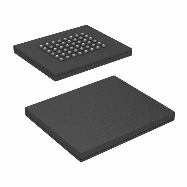
Available in non Pb-free 48-ball very fine ball grid array
(VFBGA) package.
consumption. The device can be put into standby mode reducing
power consumption by 90% when addresses are not toggling.
The device can be put into standby mode reducing power
consumption by more than 99% when deselected Chip Enable 1
(CE1) HIGH or Chip Enable 2 (CE2) LOW. The input/output pins
(I/O0 through I/O7) are placed in a high-impedance state when:
deselected Chip Enable 1 (CE1) HIGH or Chip Enable 2 (CE2)
LOW, outputs are disabled (OE HIGH), or during a write
operation (Chip Enable 1 (CE1) LOW and Chip Enable 2 (CE2)
HIGH and WE LOW).
Writing to the device is accomplished by taking Chip Enable 1
(CE1) LOW and Chip Enable 2 (CE2) HIGH and Write Enable
(WE) input LOW. Data on the eight I/O pins (I/O0 through I/O7)
is then written into the location specified on the address pins(A0
through A20).
Reading from the device is accomplished by taking Chip Enable
1 (CE1) and Output Enable (OE) LOW and Chip Enable 2 (CE2)
HIGH while forcing Write Enable (WE) HIGH. Under these
conditions, the contents of the memory location specified by the
address pins appear on the I/O pins.
The eight input/output pins (I/O0 through I/O7) are placed in a
high-impedance state when the device is deselected (CE1 LOW
and CE2 HIGH), the outputs are disabled (OE HIGH), or during
a write operation (CE1 LOW and CE2 HIGH and WE LOW). See
the Truth Table on page 10 for a complete description of read and
write modes.
Functional Description
The CY62168DV30 is a high-performance CMOS static RAMs
organized as 2048Kbit words by 8 bits. This device features
advanced circuit design to provide ultra-low active current. This
is ideal for providing More Battery Life (MoBL) in portable
applications such as cellular telephones. The device also has an
automatic power-down feature that significantly reduces power
For a complete list of related documentation, click here.
Logic Block Diagram
I/O0
Data in Drivers
I/O1
2048K x 8
ARRAY
I/O2
SENSE AMPS
ROW DECODER
A0
A1
A2
A3
A4
A5
A6
A7
A8
A9
A10
A11
A12
I/O3
I/O4
I/O5
COLUMN
DECODER
CE1
CE2
I/O6
POWER
DOWN
I/O7
A16
OE
Cypress Semiconductor Corporation
Document Number: 38-05329 Rev. *M
A17
A18
A19
A20
A13
A14
A15
WE
•
198 Champion Court
•
San Jose, CA 95134-1709
•
408-943-2600
Revised December 3, 2015
�CY62168DV30 MoBL®
Contents
Product Portfolio .............................................................. 3
Pin Configuration ............................................................. 3
Maximum Ratings ............................................................. 4
Operating Range ............................................................... 4
DC Electrical Characteristics .......................................... 4
Capacitance ...................................................................... 5
Thermal Resistance .......................................................... 5
AC Test Loads and Waveforms ....................................... 5
Data Retention Characteristics ....................................... 6
Data Retention Waveform ................................................ 6
Switching Characteristics ................................................ 7
Switching Waveforms ...................................................... 8
Truth Table ...................................................................... 10
Document Number: 38-05329 Rev. *M
Ordering Information ...................................................... 11
Ordering Code Definitions ......................................... 11
Package Diagram ............................................................ 12
Acronyms ........................................................................ 13
Document Conventions ................................................. 13
Units of Measure ....................................................... 13
Document History Page ................................................. 14
Sales, Solutions, and Legal Information ...................... 15
Worldwide Sales and Design Support ....................... 15
Products .................................................................... 15
PSoC® Solutions ...................................................... 15
Cypress Developer Community ................................. 15
Technical Support ..................................................... 15
Page 2 of 15
�CY62168DV30 MoBL®
Product Portfolio
Power Dissipation
VCC Range (V)
Product
CY62168DV30LL
Operating ICC (mA)
Speed
(ns)
Min
Typ [1]
Max
2.2
3.0
3.6
f = 1 MHz
Standby ISB2(A)
f = fMax
Typ [1]
Max
Typ [1]
Max
Typ [1]
Max
2
4
15
30
2.5
22
55
Pin Configuration
Figure 1. 48-ball VFBGA pinout (Top View) [2]
1
2
3
4
5
6
DNU
OE
A0
A1
A2
CE2
A
DNU DNU
A3
A4
CE1 DNU
B
I/O0
DNU
A5
A6
DNU
I/O4
C
VSS
I/O1
A17
A7
I/O5
VCC
D
VCC
I/O2
DNU
A16
I/O6
VSS
E
I/O3
DNU
A14
A15
DNU
I/O7
F
DNU
A20
A12
A13
WE
DNU
G
A18
A8
A9
A10
A11
A19
H
Notes
1. Typical values are included for reference only and are not guaranteed or tested. Typical values are measured at VCC = VCC(typ.), TA = 25 °C.
2. DNU pins have to be left floating or tied to VSS to ensure proper operation.
Document Number: 38-05329 Rev. *M
Page 3 of 15
�CY62168DV30 MoBL®
DC input voltage [3, 4] ...................–0.3 V to VCC(max) + 0.3 V
Maximum Ratings
Exceeding maximum ratings may shorten the useful life of the
device. User guidelines are not tested.
Storage temperature ................................ –65 °C to +150 °C
Ambient temperature with
power applied .......................................... –55 °C to +125 °C
Supply voltage to ground
potential ...................................... –0.3 V to VCC(max) + 0.3 V
DC voltage applied to outputs
in High-Z state [3, 4] ......................–0.3 V to VCC(max) + 0.3 V
Output current into outputs (LOW) ............................. 20 mA
Static discharge voltage
(per MIL-STD-883, Method 3015) .......................... > 2001 V
Latch-up current .................................................... > 200 mA
Operating Range
Range
Ambient Temperature (TA) [5]
VCC[6]
Industrial
–40 °C to +85 °C
2.2 V–3.6 V
DC Electrical Characteristics
Over the Operating Range
Parameter
VOH
Description
Output HIGH voltage
VOL
Output LOW voltage
VIH
Input HIGH voltage
Test Conditions
CY62168DV30-55
Min
Typ [7]
Max
2.2 V VCC 2.7 V IOH = 0.1 mA
2.0
–
–
2.7 V VCC 3.6 V IOH = 1.0 mA
2.4
–
–
2.2 V VCC 2.7 V IOL = 0.1 mA
–
–
0.4
2.7 V VCC 3.6 V IOL = 2.1 mA
–
–
0.4
2.2 V VCC 2.7 V
1.8
–
VCC + 0.3
2.7 V VCC 3.6 V
2.2
–
VCC + 0.3
2.2 V VCC 2.7 V
–0.3
–
0.6
2.7 V VCC 3.6 V
Unit
V
V
V
VIL
Input LOW voltage
–0.3
–
0.8
IIX
Input leakage current
GND VI VCC
–1
–
+1
A
IOZ
Output leakage current
GND VO VCC, Output disabled
–1
–
+1
A
ICC
VCC operating supply current
f = fMax = 1/tRC
–
15
30
mA
–
2
4
–
2.5
22
A
–
2.5
22
A
f = 1 MHz
ISB1
Automatic CE power-down
current – CMOS inputs
ISB2
Automatic CE power-down
current – CMOS inputs
VCC = 3.6 V,
IOUT = 0 mA,
CMOS level
CE1 VCC 0.2 V, CE2 0.2 V,
VIN VCC 0.2 V or VIN 0.2 V,
f = fMax (Address and data only),
V
f = 0 (OE, WE)
CE1 > VCC 0.2 V, CE2 0.2 V,
VIN VCC 0.2 V or VIN 0.2 V,
f = 0, VCC = 3.6 V
Notes
3. VIL(min) = –2.0 V for pulse durations less than 20 ns.
4. VIH(max) = VCC + 0.75 V for pulse durations less than 20 ns.
5. TA is the “Instant-On” case temperature.
6. Full device AC operation assumes a 100 s ramp time from 0 to VCC(min) and 100 s wait time after VCC stabilization.
7. Typical values are included for reference only and are not guaranteed or tested. Typical values are measured at VCC = VCC(typ.), TA = 25 °C.
Document Number: 38-05329 Rev. *M
Page 4 of 15
�CY62168DV30 MoBL®
Capacitance
Parameter [8]
Description
CIN
Input capacitance
COUT
Output capacitance
Test Conditions
TA = 25 °C, f = 1 MHz, VCC = VCC(typ.)
Max
Unit
8
pF
10
pF
VFBGA
Unit
55
C/W
16
C/W
Thermal Resistance
Parameter [8]
Description
JA
Thermal resistance
(junction to ambient)
JC
Thermal resistance
(junction to case)
Test Conditions
Still air, soldered on a 3 × 4.5 inch,
two-layer printed circuit board
AC Test Loads and Waveforms
Figure 2. AC Test Loads and Waveforms
R1
VCC
ALL INPUT PULSES
VCC
OUTPUT
50 pF
R2
GND
10%
90%
10%
90%
Fall time: 1 V/ns
Rise Time: 1 V/ns
INCLUDING
JIG AND
SCOPE
Equivalent to:
THEVENIN EQUIVALENT
RTH
OUTPUT
Parameters
2.5 V
VTH
3.0 V
Unit
R1
16600
1103
R2
15400
1554
RTH
8000
645
VTH
1.2
1.75
V
Note
8. Tested initially and after any design or process changes that may affect these parameters.
Document Number: 38-05329 Rev. *M
Page 5 of 15
�CY62168DV30 MoBL®
Data Retention Characteristics
Over the Operating Range
Parameter
Description
VDR
VCC for data retention
ICCDR
Data retention current
Conditions
VCC = 1.5 V,
Min
Typ [10]
Max
Unit
1.5
–
3.6
V
–
–
10
A
CE1 > VCC – 0.2 V or CE2 < 0.2 V,
VIN > VCC – 0.2 V or VIN < 0.2 V
tCDR[9]
Chip deselect to data retention
time
0
–
–
ns
tR[11]
Operation recovery time
55
–
–
ns
Data Retention Waveform
Figure 3. Data Retention Waveform
DATA RETENTION MODE
VCC
VCC(min)
tCDR
VDR 1.5 V
VCC(min)
tR
CE1
or
CE2
Notes
9. Tested initially and after any design or process changes that may affect these parameters.
10. Typical values are included for reference only and are not guaranteed or tested. Typical values are measured at VCC = VCC(typ), TA = 25 °C.
11. Full Device AC operation requires linear VCC ramp from VDR to VCC(min) > 100s or stable at VCC(min) > 100s.
Document Number: 38-05329 Rev. *M
Page 6 of 15
�CY62168DV30 MoBL®
Switching Characteristics
Over the Operating Range
Parameter [12]
Description
55 ns
Min
Max
Unit
Read Cycle
tRC
Read cycle time
55
–
ns
tAA
Address to data valid
–
55
ns
tOHA
Data hold from address change
10
–
ns
tACE
CE1 LOW and CE2 HIGH to data valid
–
55
ns
tDOE
OE LOW to data valid
–
25
ns
5
–
ns
–
20
ns
tLZOE
tHZOE
OE LOW to low Z
[13]
OE HIGH to high Z
[13, 14]
[13]
tLZCE
CE1 LOW and CE2 HIGH to low Z
10
–
ns
tHZCE
CE1 HIGH or CE2 LOW to high Z [13, 14]
–
20
ns
tPU
CE1 LOW and CE2 HIGH to power-up
0
–
ns
CE1 HIGH or CE2 LOW to power-down
–
55
ns
tPD
Write Cycle
[15, 16]
tWC
Write cycle time
55
–
ns
tSCE
CE1 LOW and CE2 HIGH to write end
40
–
ns
tAW
Address setup to write end
40
–
ns
tHA
Address hold from write end
0
–
ns
tSA
Address setup to write start
0
–
ns
tPWE
WE Pulse width
40
–
ns
tSD
Data setup to write end
25
–
ns
tHD
Data hold from write end
0
–
ns
tHZWE
WE LOW to high Z [13, 14]
–
20
ns
10
–
ns
tLZWE
WE HIGH to low Z
[13]
Notes
12. Test conditions for all parameters other than tri-state parameters assume signal transition time of 3ns or less (1V/ns), timing reference levels of VCC(typ.)/2, input pulse
levels of 0 to VCC(typ.), and output loading of the specified IOL/IOH as shown in the “AC Test Loads and Waveforms” section.
13. At any temperature and voltage condition, tHZCE is less than tLZCE, tHZOE is less than tLZOE, and tHZWE is less than tLZWE for any device.
14. tHZOE, tHZCE, and tHZWE transitions are measured when the outputs enter a high impedance state.
15. The internal write time of the memory is defined by the overlap of WE, CE1 = VIL, and CE2 = VIH. All signals must be ACTIVE to initiate a write and any of these signals
can terminate a write by going INACTIVE. The data input setup and hold timing should be referenced to the edge of the signal that terminates the write.
16. The minimum write pulse width for Write Cycle No. 3 (WE Controlled, OE LOW) should be equal to sum of tSD and tHZWE.
Document Number: 38-05329 Rev. *M
Page 7 of 15
�CY62168DV30 MoBL®
Switching Waveforms
Figure 4. Read Cycle No. 1 (Address Transition Controlled) [17, 18]
tRC
ADDRESS
tOHA
DATA OUT
tAA
PREVIOUS DATA VALID
DATA VALID
Figure 5. Read Cycle No. 2 (OE Controlled) [18, 19]
ADDRESS
tRC
CE1
CE2
tACE
OE
tHZOE
tDOE
tHZCE
tLZOE
HIGH IMPEDANCE
DATA OUT
DATA VALID
tLZCE
tPD
tPU
VCC
SUPPLY
CURRENT
HIGH
IMPEDANCE
50%
50%
ICC
ISB
Figure 6. Write Cycle No. 1 (WE Controlled) [20, 21, 22]
tWC
ADDRESS
tSCE
CE1
CE2
tAW
tSA
tHA
tPWE
WE
OE
tSD
DATA I/O
See Note 23
tHD
VALID DATA
tHZOE
Notes
17. Device is continuously selected. OE, CE1 = VIL, CE2 = VIH.
18. WE is HIGH for read cycle.
19. Address valid prior to or coincident with CE1 transition LOW and CE2 transition HIGH.
20. The internal write time of the memory is defined by the overlap of WE, CE1 = VIL, and CE2 = VIH. All signals must be ACTIVE to initiate a write and any of these
signals can terminate a write by going INACTIVE. The data input setup and hold timing should be referenced to the edge of the signal that terminates the write.
21. Data I/O is high impedance if OE = VIH.
22. If CE1 goes HIGH or CE2 goes LOW simultaneously with WE HIGH, the output remains in high-impedance state.
23. During this period, the I/Os are in output state and input signals should not be applied.
Document Number: 38-05329 Rev. *M
Page 8 of 15
�CY62168DV30 MoBL®
Switching Waveforms (continued)
Figure 7. Write Cycle No. 2 (CE1 or CE2 Controlled) [24, 25, 26]
tWC
ADDRESS
tSCE
CE1
tSA
CE2
tAW
tHA
tPWE
WE
OE
tSD
DATA I/O
tHD
VALID DATA
Figure 8. Write Cycle No. 3 (WE Controlled, OE LOW) [27]
tWC
ADDRESS
tSCE
CE1
CE2
tAW
tSA
tHA
tPWE
WE
tSD
DATA I/O
See Note 28
tHD
VALID DATA
tHZWE
tLZWE
Notes
24. The internal write time of the memory is defined by the overlap of WE, CE1 = VIL, and CE2 = VIH. All signals must be ACTIVE to initiate a write and any of these signals
can terminate a write by going INACTIVE. The data input setup and hold timing should be referenced to the edge of the signal that terminates the write.
25. Data I/O is high impedance if OE = VIH.
26. If CE1 goes HIGH or CE2 goes LOW simultaneously with WE HIGH, the output remains in high-impedance state.
27. The minimum write cycle pulse width should be equal to sum of tSD and tHZWE.
28. During this period, the I/Os are in output state and input signals should not be applied.
Document Number: 38-05329 Rev. *M
Page 9 of 15
�CY62168DV30 MoBL®
Truth Table
CE1
CE2
WE
OE
Inputs/Outputs
H
X
X
X
High Z
Deselect/Power-down
Standby (ISB)
X
L
X
X
High Z
Deselect/Power-down
Standby (ISB)
L
H
H
L
Data out (I/O0–I/O7)
Read
Active (ICC)
L
H
L
X
Data in (I/O0–I/O7)
Write
Active (ICC)
L
H
H
H
High Z
Output disabled
Active (ICC)
Document Number: 38-05329 Rev. *M
Mode
Power
Page 10 of 15
�CY62168DV30 MoBL®
Ordering Information
The following table contains only the parts that are currently available. If you do not see what you are looking for, contact your local
sales representative. For more information, visit the Cypress website at http://www.cypress.com and see product summary page at
http://www.cypress.com/products. Cypress maintains a worldwide network of offices, solution centers, manufacturers representatives
and distributors. To find the office closest to you, visit us at http://www.cypress.com/go/datasheet/offices.
Speed
(ns)
55
Ordering Code
CY62168DV30LL-55BVI
Package
Diagram
Package Type
51-85178 48-ball FBGA (8 × 9.5 × 1 mm)
Operating
Range
Industrial
Please contact your local Cypress sales representative for availability of these parts.
Ordering Code Definitions
CY 621 6
8
D
V30 LL - 55
BV
I
Temperature Range: I = Industrial
Package Type:
BV = 48-ball FBGA
Speed Grade: 55 ns
Low Power
Voltage Range: 3 V Typical
Process Technology: 130 nm Technology
Bus Width: 8 = × 8
Density: 6 = 16-Mbit
Family Code: 621 = MoBL SRAM family
Company ID: CY = Cypress
Document Number: 38-05329 Rev. *M
Page 11 of 15
�CY62168DV30 MoBL®
Package Diagram
Figure 9. 48-ball VFBGA (8 × 9.5 × 1.0 mm) BV48B Package Outline, 51-85178
51-85178 *C
Document Number: 38-05329 Rev. *M
Page 12 of 15
�CY62168DV30 MoBL®
Acronyms
Acronym
Document Conventions
Description
Units of Measure
CMOS
Complementary Metal Oxide Semiconductor
I/O
Input/Output
°C
degree Celsius
SRAM
Static Random Access Memory
MHz
megahertz
VFBGA
Very Fine-Pitch Ball Grid Array
A
microampere
Thin Small Outline Package
mA
milliampere
ns
nanosecond
ohm
pF
picofarad
V
volt
W
watt
TSOP
Document Number: 38-05329 Rev. *M
Symbol
Unit of Measure
Page 13 of 15
�CY62168DV30 MoBL®
Document History Page
Document Title: CY62168DV30 MoBL®, 16-Mbit (2 M × 8) Static RAM
Document Number: 38-05329
Revision
ECN
Orig. of
Change
Submission
Date
**
118409
GUG
09/30/02
New data sheet.
*A
123693
DPM
02/05/03
Changed status from Advance Information to Preliminary.
Added Package Diagram.
Description of Change
*B
126556
DPM
04/24/03
Minor change: Change sunset owner from DPM to HRT
*C
132869
XRJ
01/15/04
Changed status from Preliminary to Final.
*D
272589
PCI
See ECN
Added Pb-free package related information in all instances across the
document.
Updated Ordering Information.
*E
335864
PCI
See ECN
Updated Pin Configuration:
Updated Figure 1 (Added Address A20 to ball G2).
Updated Ordering Information:
Removed redundant packages.
*F
492895
VKN
See ECN
Changed address of Cypress Semiconductor Corporation on Page 1 from
“3901 North First Street” to “198 Champion Court”
Removed 70 ns speed bin related information in all instances across the
document.
Removed Low Power parts related information in all instances across the
document.
Updated Ordering Information.
*G
2914085
NIKM
04/15/10
Updated Ordering Information:
Removed inactive parts.
Updated Package Diagram.
*H
3070774
RAME
10/27/10
Changed all table notes to footnotes in all instances across the document.
Added Ordering Code Definitions.
Added Acronyms and Units of Measure.
Updated to new template.
*I
3090588
AJU
11/19/10
Post to external web.
*J
3329789
RAME
07/27/11
Updated Functional Description:
Removed Note “For best-practice recommendations, please refer to the
Cypress application note entitled System Design Guidelines, available at
http://www.cypress.com website” and its reference.
Updated to new template.
*K
4192919
VINI
11/15/2013
Updated Package Diagram:
spec 51-85178 – Changed revision from *A to *C.
Updated to new template.
Completing Sunset Review.
*L
4574377
VINI
11/19/2014
Updated Functional Description:
Added “For a complete list of related documentation, click here.” at the end.
*M
5036233
VINI
12/03/2015
Updated Switching Characteristics:
Added Note 16 and referred the same note in “Write Cycle”.
Updated Switching Waveforms:
Added Note 27 and referred the same note in Figure 8.
Updated to new template.
Completing Sunset Review.
Document Number: 38-05329 Rev. *M
Page 14 of 15
�CY62168DV30 MoBL®
Sales, Solutions, and Legal Information
Worldwide Sales and Design Support
Cypress maintains a worldwide network of offices, solution centers, manufacturer’s representatives, and distributors. To find the office
closest to you, visit us at Cypress Locations.
PSoC® Solutions
Products
Automotive
Clocks & Buffers
Interface
Lighting & Power Control
Memory
cypress.com/go/automotive
cypress.com/go/clocks
cypress.com/go/interface
cypress.com/go/powerpsoc
cypress.com/go/memory
PSoC
cypress.com/go/psoc
Touch Sensing
cypress.com/go/touch
USB Controllers
Wireless/RF
psoc.cypress.com/solutions
PSoC 1 | PSoC 3 | PSoC 4 | PSoC 5LP
Cypress Developer Community
Community | Forums | Blogs | Video | Training
Technical Support
cypress.com/go/support
cypress.com/go/USB
cypress.com/go/wireless
© Cypress Semiconductor Corporation, 2002-2015. The information contained herein is subject to change without notice. Cypress Semiconductor Corporation assumes no responsibility for the use of
any circuitry other than circuitry embodied in a Cypress product. Nor does it convey or imply any license under patent or other rights. Cypress products are not warranted nor intended to be used for
medical, life support, life saving, critical control or safety applications, unless pursuant to an express written agreement with Cypress. Furthermore, Cypress does not authorize its products for use as
critical components in life-support systems where a malfunction or failure may reasonably be expected to result in significant injury to the user. The inclusion of Cypress products in life-support systems
application implies that the manufacturer assumes all risk of such use and in doing so indemnifies Cypress against all charges.
Any Source Code (software and/or firmware) is owned by Cypress Semiconductor Corporation (Cypress) and is protected by and subject to worldwide patent protection (United States and foreign),
United States copyright laws and international treaty provisions. Cypress hereby grants to licensee a personal, non-exclusive, non-transferable license to copy, use, modify, create derivative works of,
and compile the Cypress Source Code and derivative works for the sole purpose of creating custom software and or firmware in support of licensee product to be used only in conjunction with a Cypress
integrated circuit as specified in the applicable agreement. Any reproduction, modification, translation, compilation, or representation of this Source Code except as specified above is prohibited without
the express written permission of Cypress.
Disclaimer: CYPRESS MAKES NO WARRANTY OF ANY KIND, EXPRESS OR IMPLIED, WITH REGARD TO THIS MATERIAL, INCLUDING, BUT NOT LIMITED TO, THE IMPLIED WARRANTIES
OF MERCHANTABILITY AND FITNESS FOR A PARTICULAR PURPOSE. Cypress reserves the right to make changes without further notice to the materials described herein. Cypress does not
assume any liability arising out of the application or use of any product or circuit described herein. Cypress does not authorize its products for use as critical components in life-support systems where
a malfunction or failure may reasonably be expected to result in significant injury to the user. The inclusion of Cypress’ product in a life-support systems application implies that the manufacturer
assumes all risk of such use and in doing so indemnifies Cypress against all charges.
Use may be limited by and subject to the applicable Cypress software license agreement.
Document Number: 38-05329 Rev. *M
Revised December 3, 2015
Page 15 of 15
MoBL is a registered trademark, and More Battery Life is a trademark, of Cypress Semiconductor. All product and company names mentioned in this document are trademarks of their respective holders
�


 工商网监
湘ICP备2023018690号
工商网监
湘ICP备2023018690号
