CY62256VN
256-Kbit (32 K × 8) Static RAM
256-Kbit (32 K × 8) Static RAM
Features
Functional Description
■
Temperature ranges
❐ Commercial: 0 °C to +70 °C
❐ Industrial: –40 °C to +85 °C
❐ Automotive-A: –40 °C to +85 °C
❐ Automotive-E: –40 °C to +125 °C
The CY62256VN family is composed of two high performance
CMOS static RAM’s organized as 32K words by 8 bits. Easy
memory expansion is provided by an active LOW chip enable
(CE) and active LOW output enable (OE) and tristate drivers.
These devices have an automatic power-down feature, reducing
the power consumption by over 99% when deselected.
■
Speed: 70 ns
■
Low voltage range: 2.7 V to 3.6 V
■
Low active power and standby power
■
Easy memory expansion with CE and OE features
■
TTL compatible inputs and outputs
■
Automatic power-down when deselected
■
CMOS for optimum speed and power
An active LOW write enable signal (WE) controls the
writing/reading operation of the memory. When CE and WE
inputs are both LOW, data on the eight data input/output pins
(I/O0 through I/O7) is written into the memory location addressed
by the address present on the address pins (A0 through A14).
Reading the device is accomplished by selecting the device and
enabling the outputs, CE and OE active LOW, while WE remains
inactive or HIGH. Under these conditions, the contents of the
location addressed by the information on address pins are
present on the eight data input/output pins.
■
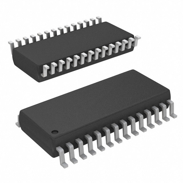
Available in standard Pb-free and non Pb-free 28-pin (300-mil)
narrow SOIC, 28-pin TSOP-I, and 28-pin reverse TSOP-I
packages
The input/output pins remain in a high impedance state unless
the chip is selected, outputs are enabled, and write enable (WE)
is HIGH.
For a complete list of related documentation, click here.
Logic Block Diagram
I/O0
INPUTBUFFER
I/O1
32K x 8
ARRAY
I/O2
SENSE AMPS
ROW DECODER
A10
A9
A8
A7
A6
A5
A4
A3
A2
I/O3
I/O4
I/O5
CE
WE
COLUMN
DECODER
I/O6
POWER
DOWN
I/O7
Cypress Semiconductor Corporation
Document Number: 001-06512 Rev. *H
•
A12
A11
A1
A0
A13
A14
OE
198 Champion Court
•
San Jose, CA 95134-1709
•
408-943-2600
Revised January 16, 2015
�CY62256VN
Contents
Product Portfolio .............................................................. 3
Pin Configurations ........................................................... 3
Pin Definitions .................................................................. 3
Maximum Ratings ............................................................. 4
Operating Range ............................................................... 4
Electrical Characteristics ................................................. 4
Capacitance ...................................................................... 5
Thermal Resistance .......................................................... 5
AC Test Loads and Waveforms ....................................... 5
Data Retention Characteristics ....................................... 6
Data Retention Waveform ................................................ 6
Switching Characteristics ................................................ 7
Switching Waveforms ...................................................... 8
Typical DC and AC Characteristics .............................. 10
Truth Table ...................................................................... 11
Document Number: 001-06512 Rev. *H
Ordering Information ...................................................... 12
Ordering Code Definitions ......................................... 12
Package Diagrams .......................................................... 13
Acronyms ........................................................................ 15
Document Conventions ................................................. 15
Units of Measure ....................................................... 15
Document History Page ................................................. 16
Sales, Solutions, and Legal Information ...................... 17
Worldwide Sales and Design Support ....................... 17
Products .................................................................... 17
PSoC® Solutions ...................................................... 17
Cypress Developer Community ................................. 17
Technical Support ..................................................... 17
Page 2 of 17
�CY62256VN
Product Portfolio
Product
Power Dissipation
VCC Range (V)
Range
Operating, ICC (mA)
Standby, ISB2 (A)
Min
Typ[1]
Max
Typ[1]
Max
Typ[1]
Max
CY62256VNLL
Commercial
2.7
3.0
3.6
11
30
0.1
5
CY62256VNLL
Industrial
2.7
3.0
3.6
11
30
0.1
10
CY62256VNLL
Automotive-A
2.7
3.0
3.6
11
30
0.1
10
CY62256VNLL
Automotive-E
2.7
3.0
3.6
11
30
0.1
130
Pin Configurations
Figure 1. 28-pin SOIC and 28-pin TSOP I pinouts
Narrow SOIC
Top View
A5
A6
A7
A8
A9
A10
A11
A12
A13
A14
I/O0
I/O1
I/O2
GND
VCC
WE
A4
A3
A2
A1
OE
A0
CE
I/O7
I/O6
I/O5
I/O4
I/O3
28
27
26
25
24
23
22
21
20
19
18
17
16
15
1
2
3
4
5
6
7
8
9
10
11
12
13
14
OE
A1
A2
A3
A4
WE
VCC
A5
A6
A7
A8
A9
A10
A11
21
22
23
24
25
26
27
28
1
2
3
4
5
6
7
TSOP I
Top View
(not to scale)
20
19
18
17
16
15
14
13
12
11
10
9
8
A0
CE
I/O7
I/O6
I/O5
I/O4
I/O3
GND
I/O2
I/O1
I/O0
A14
A13
A12
A11
A10
A9
A8
A7
A6
A5
VCC
WE
A4
A3
A2
A1
OE
7
6
8
9
5
4
3
2
10
11
12
13
14
15
16
17
18
1
28
27
26
25
24
23
22
TSOP I
Reverse Pinout
Top View
(not to scale)
19
20
21
A12
A13
A14
I/O0
I/O1
I/O2
GND
I/O3
I/O4
I/O5
I/O6
I/O7
CE
A0
Pin Definitions
Pin Number
Type
Description
1–10, 21, 23–26 Input
A0–A14. Address inputs
11–13, 15–19
Input/Output
I/O0–I/O7. Data lines. Used as input or output lines depending on operation.
27
Input/Control
WE. When selected LOW, a WRITE is conducted. When selected HIGH, a READ is conducted.
20
Input/Control
CE. When LOW, selects the chip. When HIGH, deselects the chip.
22
Input/Control
OE. Output Enable. Controls the direction of the I/O pins. When LOW, the I/O pins behave as
outputs. When deasserted HIGH, I/O pins are tristated, and act as input data pins.
14
Ground
GND. Ground for the device
28
Power Supply
VCC. Power supply for the device
Note
1. Typical values are included for reference only and are not guaranteed or tested. Typical values are measured at VCC = VCC Typ, TA = 25 °C, and tAA = 70 ns.
Document Number: 001-06512 Rev. *H
Page 3 of 17
�CY62256VN
Maximum Ratings
Static discharge voltage
(per MIL-STD-883, method 3015) ......................... > 2001 V
Exceeding maximum ratings may shorten the useful life of the
device. User guidelines are not tested.
Latch-up current ................................................... > 200 mA
Storage temperature ................................ –65 °C to +150 °C
Operating Range
Ambient temperature with
power applied .......................................... –55 °C to +125 °C
Supply voltage to ground potential
(pin 28 to pin 14) [2] .....................................–0.5 V to +4.6 V
Device
Range
CY62256VN Commercial
DC voltage applied to outputs
in high Z State [2] ................................ –0.5 V to VCC + 0.5 V
DC input voltage [2] ............................. –0.5 V to VCC + 0.5 V
Ambient
Temperature (TA) [3]
VCC
0 °C to +70 °C
2.7 V to
3.6 V
Industrial
–40 °C to +85 °C
Automotive-A
–40 °C to +85 °C
Automotive-E
–40 °C to +125 °C
Output current into outputs (LOW) ............................. 20 mA
Electrical Characteristics
Over the Operating Range
Parameter
Description
Test Conditions
-70
Min
Typ [4]
Max
Unit
VOH
Output HIGH voltage
IOH = 1.0 mA
VCC = 2.7 V
2.4
–
–
V
VOL
Output LOW voltage
IOL = 2.1 mA
VCC = 2.7 V
–
–
0.4
V
VIH
Input HIGH voltage
2.2
–
VCC + 0.3
V
VIL
Input LOW voltage
IIX
Input leakage current
GND VIN VCC
–0.5
–
0.8
V
Commercial/
Industrial/
Automotive-A
–1
–
+1
A
Automotive-E
–10
–
+10
A
–
+1
A
IOZ
Output leakage current
GND VIN VCC,
Output Disabled
Commercial/
Industrial/
Automotive-A
–1
Automotive-E
–10
–
+10
A
ICC
VCC operating supply current
VCC = 3.6 V,
IOUT = 0 mA,
f = fMAX = 1/tRC
All ranges
–
11
30
mA
ISB1
Automatic CE power-down
current - TTL inputs
VCC = 3.6 V,
CE VIH,
VIN VIH or
VIN VIL,
f = fMAX
All ranges
–
100
300
A
ISB2
Automatic CE power-down
current - CMOS inputs
VCC = 3.6 V,
Commercial
CE VCC – 0.3 V,
Industrial/
VIN VCC – 0.3 V or
Automotive-A
VIN 0.3 V, f = 0
Automotive-E
–
0.1
5
A
–
10
–
130
Notes
2. VIL (min) = –2.0 V for pulse durations of less than 20 ns.
3. TA is the “Instant-On” case temperature.
4. Typical values are included for reference only and are not guaranteed or tested. Typical values are measured at VCC = VCC Typ, TA = 25 °C, and tAA = 70 ns.
Document Number: 001-06512 Rev. *H
Page 4 of 17
�CY62256VN
Capacitance
Parameter [5]
Description
CIN
Input capacitance
COUT
Output capacitance
Test Conditions
TA = 25 °C, f = 1 MHz, VCC = 3.0 V
Max
Unit
6
pF
8
pF
Thermal Resistance
Parameter [5]
Description
JA
Thermal resistance
(junction to ambient)
JC
Thermal resistance
(junction to case)
Test Conditions
Still air, soldered on a
3 × 4.5 inch, two-layer
printed circuit board
SOIC
TSOPI
RTSOPI
Unit
68.45
87.62
87.62
C/W
26.94
23.73
23.73
C/W
AC Test Loads and Waveforms
Figure 2. AC Test Loads and Waveforms
R1
VCC
ALL INPUT PULSES
OUTPUT
VCC
50 pF
INCLUDING
JIG AND
SCOPE
10%
R2
90%
GND
5 ns
5 ns
Equivalent to:
90%
10%
THÉVENIN EQUIVALENT
Rth
OUTPUT
Vth
Parameter
Value
Units
R1
1100
Ohms
R2
1500
Ohms
RTH
645
Ohms
VTH
1.750
Volts
Note
5. Tested initially and after any design or process changes that may affect these parameters.
Document Number: 001-06512 Rev. *H
Page 5 of 17
�CY62256VN
Data Retention Characteristics
Over the Operating Range
Parameter
Conditions[6]
Description
VDR
VCC for data retention
ICCDR
Data retention current
VCC = 1.4 V,
Commercial
CE VCC – 0.3 V, Industrial/
VIN VCC – 0.3 V Automotive-A
or VIN 0.3 V
Automotive-E
Min
Typ [7]
Max
Unit
1.4
–
–
V
–
0.1
3
A
–
6
–
50
tCDR[6]
Chip deselect to data retention
time
0
–
–
ns
tR[8]
Operation recovery time
70
–
–
ns
Data Retention Waveform
Figure 3. Data Retention Waveform
DATA RETENTION MODE
1.8 V
VCC
tCDR
VDR 1.4 V
1.8 V
tR
CE
Notes
6. No input may exceed VCC + 0.3 V.
7. Typical values are included for reference only and are not guaranteed or tested. Typical values are measured at VCC = VCC Typ, TA = 25 °C, and tAA = 70 ns.
8. Tested initially and after any design or process changes that may affect these parameters.
Document Number: 001-06512 Rev. *H
Page 6 of 17
�CY62256VN
Switching Characteristics
Over the Operating Range
Parameter [9]
Description
CY62256VN-70
Min
Max
Unit
Read Cycle
tRC
Read cycle time
70
–
ns
tAA
Address to data valid
–
70
ns
tOHA
Data hold from address change
10
–
ns
tACE
CE LOW to data valid
–
70
ns
tDOE
OE LOW to data valid
–
35
ns
[10]
5
–
ns
Z[10, 11]
–
25
ns
tLZOE
tHZOE
OE LOW to low Z
OE HIGH to high
Z[10]
tLZCE
CE LOW to low
10
–
ns
tHZCE
CE HIGH to high Z[10, 11]
–
25
ns
tPU
CE LOW to power-up
0
–
ns
CE HIGH to power-down
–
70
ns
tPD
Write Cycle
[12, 13]
tWC
Write cycle time
70
–
ns
tSCE
CE LOW to write end
60
–
ns
tAW
Address setup to write end
60
–
ns
tHA
Address hold from write end
0
–
ns
tSA
Address setup to write start
0
–
ns
tPWE
WE pulse width
50
–
ns
tSD
Data setup to write end
30
–
ns
tHD
Data hold from write end
0
–
ns
tHZWE
WE LOW to high Z[10, 11]
–
25
ns
10
–
ns
tLZWE
[10]
WE HIGH to low Z
Notes
9. Test conditions assume signal transition time of 5 ns or less timing reference levels of VCC/2, input pulse levels of 0 to VCC, and output loading of the specified IOL/IOH
and 100-pF load capacitance.
10. At any temperature and voltage condition, tHZCE is less than tLZCE, tHZOE is less than tLZOE, and tHZWE is less than tLZWE for any device.
11. tHZOE, tHZCE, and tHZWE are specified with CL = 5 pF as in (b) of AC Test Loads. Transition is measured ± 200 mV from steady-state voltage.
12. The internal write time of the memory is defined by the overlap of CE LOW and WE LOW. Both signals must be LOW to initiate a write and either signal can terminate
a write by going HIGH. The data input set-up and hold timing should be referenced to the rising edge of the signal that terminates the write.
13. The minimum write cycle time for Write Cycle No. 3 (WE Controlled, OE LOW) is the sum of tHZWE and tSD.
Document Number: 001-06512 Rev. *H
Page 7 of 17
�CY62256VN
Switching Waveforms
Figure 4. Read Cycle No. 1 [14, 15]
tRC
ADDRESS
tAA
tOHA
DATA OUT
PREVIOUS DATA VALID
DATA VALID
Figure 5. Read Cycle No. 2 [15, 16]
t RC
CE
tACE
OE
DATA OUT
t HZOE
tHZCE
tDOE
t LZOE
HIGH IMPEDANCE
HIGH
IMPEDANCE
DATA VALID
tLZCE
VCC
SUPPLY
CURRENT
t PD
t PU
ICC
50%
50%
ISB
Figure 6. Write Cycle No. 1 (WE Controlled) [17, 18, 19]
tWC
ADDRESS
CE
tAW
tSA
WE
tHA
t PWE
OE
tSD
DATA I/O
NOTE 20
tHD
DATAINVALID
t HZOE
Notes
14. Device is continuously selected. OE, CE = VIL.
15. WE is HIGH for read cycle.
16. Address valid prior to or coincident with CE transition LOW.
17. The internal write time of the memory is defined by the overlap of CE LOW and WE LOW. Both signals must be LOW to initiate a write and either signal can terminate
a write by going HIGH. The data input set-up and hold timing should be referenced to the rising edge of the signal that terminates the write.
18. Data I/O is high impedance if OE = VIH.
19. If CE goes HIGH simultaneously with WE HIGH, the output remains in a high impedance state.
20. During this period, the I/Os are in output state and input signals should not be applied.
Document Number: 001-06512 Rev. *H
Page 8 of 17
�CY62256VN
Switching Waveforms (continued)
Figure 7. Write Cycle No. 2 (CE Controlled) [21, 22, 23]
tWC
ADDRESS
tSCE
CE
tSA
tAW
tHA
WE
tSD
DATA I/O
t HD
DATAINVALID
Figure 8. Write Cycle No. 3 (WE Controlled, OE LOW) [23, 24]
tWC
ADDRESS
CE
tAW
t HA
tSA
WE
tSD
DATA I/O
NOTE 25
t HZWE
t HD
DATA INVALID
tLZWE
Notes
21. The internal write time of the memory is defined by the overlap of CE LOW and WE LOW. Both signals must be LOW to initiate a write and either signal can terminate
a write by going HIGH. The data input set-up and hold timing should be referenced to the rising edge of the signal that terminates the write.
22. Data I/O is high impedance if OE = VIH.
23. If CE goes HIGH simultaneously with WE HIGH, the output remains in a high impedance state.
24. The minimum write cycle time for write cycle No. 3 (WE Controlled, OE LOW) is the sum of tHZWE and tSD.
25. During this period, the I/Os are in output state and input signals should not be applied.
Document Number: 001-06512 Rev. *H
Page 9 of 17
�CY62256VN
Typical DC and AC Characteristics
1.4
1.6
1.4
1.2
2.5
1.0
2.0
TA= 25C
0.4
0.2
0.0
25
125
1.6
2.0
1.4
NORMALIZED tAA
VCC = 3.0V
TA = 25C
0.0
1.65
1.2
1.0
0.8
0.5
2.1
2.6
3.1
3.6
0.6
55
25
125
OUTPUT SOURCE CURRENT (mA)
3.
3V
105
OUTPUT SINK CURRENT
14 vs. OUTPUT VOLTAGE
12
10
8
6
4
TA = 25°C
2
0
0.0
1.0
2.0
3.0
OUTPUT VOLTAGE (V)
AMBIENT TEMPERATURE (C)
SUPPLY VOLTAGE (V)
25
AMBIENT TEMPERATURE (C)
NORMALIZED ACCESS TIME
vs. AMBIENT TEMPERATURE
2.5
ISB
–0.5
55
AMBIENT TEMPERATURE (C)
SUPPLY VOLTAGE (V)
1.0
1.0
0.5
NORMALIZED ACCESS TIME
vs. SUPPLY VOLTAGE
1.5
1.5
0.4
0.0
55
3.6
3.2
2.8
2.4
2.0
1.8
1.6
0.6
OUTPUT SINK CURRENT (mA)
0.6
0.8
=
0.8
cc
1.0
V
1.2
3.0
VCC = 3.0V
ISB2 A
NORMALIZED ICC
NORMALIZED ICC
1.8
0.2
NORMALIZED tAA
STANDBY CURRENT
vs. AMBIENT TEMPERATURE
NORMALIZED SUPPLY CURRENT
vs. AMBIENT TEMPERATURE
NORMALIZED SUPPLY CURRENT
vs. SUPPLY VOLTAGE
OUTPUT SOURCE CURRENT
vs. OUTPUT VOLTAGE
–14
–12
–10
–8
–6
TA = 25°C
–4
0
0.0
0.5
1.0
1.5
2
2.5
OUTPUT VOLTAGE (V)
Document Number: 001-06512 Rev. *H
Page 10 of 17
�CY62256VN
Typical DC and AC Characteristics (continued)
TYPICAL ACCESS TIME CHANGE
vs. OUTPUT LOADING
NORMALIZED ICC vs. CYCLE TIME
1.25
NORMALIZED ICC
DELTA tAA (ns)
30.0
25.0 T = 25C
A
VCC = 3V
20.0
15.0
10.0
VCC = 3.0V
1.00
TA = 25C
VIN = 0.5V
0.75
5.0
0.0
0
200
400
600
0.50
1
800 1000
10
20
30
CYCLE FREQUENCY (MHz)
CAPACITANCE (pF)
Truth Table
CE
WE
OE
Inputs/Outputs
H
X
X
High Z
Deselect/power-down
Standby (ISB)
L
H
L
Data out
Read
Active (ICC)
L
L
X
Data in
Write
Active (ICC)
L
H
H
High Z
Deselect, output disabled
Active (ICC)
Document Number: 001-06512 Rev. *H
Mode
Power
Page 11 of 17
�CY62256VN
Ordering Information
Speed
(ns)
70
Ordering Code
Package
Diagram
CY62256VNLL-70ZXC
51-85071
28-pin TSOP I (Pb-free)
CY62256VNLL-70SNXI
51-85092
28-pin SNC (300 Mils) Narrow Body (Pb-free)
CY62256VNLL-70ZXI
51-85071
28-pin TSOP I (Pb-free)
CY62256VNLL-70ZRXI
51-85074
28-pin Reverse TSOP I (Pb-free)
CY62256VNLL-70SNXE
51-85092
28-pin SNC (300 Mils) Narrow Body (Pb-free)
CY62256VNLL-70ZXE
51-85071
28-pin TSOP I (Pb-free)
Package Type
Operating
Range
Commercial
Industrial
Automotive-E
Ordering Code Definitions
CY 62 256 V
N LL - 70 XXX
X
Temperature Grade: X = C or I or E
C = Commercial = 0 °C to +70 °C; I = Industrial = –40 °C to +85 °C;
E = Automotive-E = –40 °C to +125 °C
Package Type: XXX = ZX or SNX or ZRX
ZX = 28-pin TSOP I (Pb-free)
SNX = 28-pin SNC (Pb-free)
ZRX = 28-pin Reverse TSOP I (Pb-free)
Speed Grade: 70 ns
Low Power
Nitride Seal Mask fix
Voltage Range (3 V Typical)
Density: 256 kbit
Family Code: MoBL SRAM family
Company ID: CY = Cypress
Document Number: 001-06512 Rev. *H
Page 12 of 17
�CY62256VN
Package Diagrams
Figure 9. 28-pin SNC (300 Mils) SN28.3 (Narrow Body) Package Outline, 51-85092
51-85092 *E
Figure 10. 28-pin TSOP 1 (8 × 13.4 × 1.2 mm) Z28 (Standard) Package Outline, 51-85071
51-85071 *J
Document Number: 001-06512 Rev. *H
Page 13 of 17
�CY62256VN
Package Diagrams
Figure 11. 28-pin TSOP I (8 × 13.4 mm) Package Outline - Reverse, 51-85074
51-85074 *H
Document Number: 001-06512 Rev. *H
Page 14 of 17
�CY62256VN
Acronyms
Acronym
Document Conventions
Description
Units of Measure
CMOS
Complementary Metal Oxide Semiconductor
I/O
Input/Output
°C
degree Celsius
SRAM
Static Random Access Memory
A
microampere
TSOP
Thin Small Outline Package
mA
milliampere
VFBGA
Very Fine-Pitch Ball Grid Array
MHz
megahertz
ns
nanosecond
ohm
pF
picofarad
V
volt
W
watt
Document Number: 001-06512 Rev. *H
Symbol
Unit of Measure
Page 15 of 17
�CY62256VN
Document History Page
Document Title: CY62256VN, 256-Kbit (32 K × 8) Static RAM
Document Number: 001-06512
Revision
ECN
Orig. of
Change
Submission
Date
**
426504
NXR
See ECN
New data sheet
*A
488954
NXR
See ECN
Added Automotive product
Updated ordering Information table
Corrected VIL description in the Electrical Characteristics table
Description of Change
*B
2769239
VKN / AESA
09/25/09
*C
2901521
AJU
03/30/2010
Removed inactive parts from Ordering Information.
Updated Package Diagram.
*D
3119519
AJU
01/04/2011
Updated Ordering Information.
Added Ordering Code Definitions.
*E
3329873
RAME
07/27/11
*F
4122787
VINI
09/13/2013
Updated Package Diagrams:
spec 51-85092 – Changed revision from *C to *E.
Updated in new template.
Completing Sunset Review.
*G
4525875
VINI
10/06/2014
Updated Maximum Ratings:
Referred Note 2 in “Supply voltage to ground potential (pin 28 to pin 14)”.
Updated Package Diagrams:
spec 51-85071 – Changed revision from *I to *J.
spec 51-85074 – Changed revision from *G to *H.
Completing Sunset Review.
*H
4576406
VINI
01/16/2015
Added related documentation hyperlink in page 1.
Added Note 13 in Switching Characteristics.
Added note reference 13 in the Switching Characteristics table.
Document Number: 001-06512 Rev. *H
Updated template and styles according to current Cypress standards.
Added acronyms and units.
Removed reference to AN1064 SRAM system guidelines.
Updated operation recovery time parameter under Data Retention
Characteristics on page 6.
Page 16 of 17
�CY62256VN
Sales, Solutions, and Legal Information
Worldwide Sales and Design Support
Cypress maintains a worldwide network of offices, solution centers, manufacturer’s representatives, and distributors. To find the office
closest to you, visit us at Cypress Locations.
PSoC® Solutions
Products
Automotive
Clocks & Buffers
Interface
Lighting & Power Control
Memory
PSoC
Touch Sensing
USB Controllers
Wireless/RF
cypress.com/go/automotive
cypress.com/go/clocks
cypress.com/go/interface
cypress.com/go/powerpsoc
psoc.cypress.com/solutions
PSoC 1 | PSoC 3 | PSoC 4 | PSoC 5LP
Cypress Developer Community
Community | Forums | Blogs | Video | Training
cypress.com/go/memory
cypress.com/go/psoc
cypress.com/go/touch
Technical Support
cypress.com/go/support
cypress.com/go/USB
cypress.com/go/wireless
© Cypress Semiconductor Corporation, 2006-2015. The information contained herein is subject to change without notice. Cypress Semiconductor Corporation assumes no responsibility for the use of
any circuitry other than circuitry embodied in a Cypress product. Nor does it convey or imply any license under patent or other rights. Cypress products are not warranted nor intended to be used for
medical, life support, life saving, critical control or safety applications, unless pursuant to an express written agreement with Cypress. Furthermore, Cypress does not authorize its products for use as
critical components in life-support systems where a malfunction or failure may reasonably be expected to result in significant injury to the user. The inclusion of Cypress products in life-support systems
application implies that the manufacturer assumes all risk of such use and in doing so indemnifies Cypress against all charges.
Any Source Code (software and/or firmware) is owned by Cypress Semiconductor Corporation (Cypress) and is protected by and subject to worldwide patent protection (United States and foreign),
United States copyright laws and international treaty provisions. Cypress hereby grants to licensee a personal, non-exclusive, non-transferable license to copy, use, modify, create derivative works of,
and compile the Cypress Source Code and derivative works for the sole purpose of creating custom software and or firmware in support of licensee product to be used only in conjunction with a Cypress
integrated circuit as specified in the applicable agreement. Any reproduction, modification, translation, compilation, or representation of this Source Code except as specified above is prohibited without
the express written permission of Cypress.
Disclaimer: CYPRESS MAKES NO WARRANTY OF ANY KIND, EXPRESS OR IMPLIED, WITH REGARD TO THIS MATERIAL, INCLUDING, BUT NOT LIMITED TO, THE IMPLIED WARRANTIES
OF MERCHANTABILITY AND FITNESS FOR A PARTICULAR PURPOSE. Cypress reserves the right to make changes without further notice to the materials described herein. Cypress does not
assume any liability arising out of the application or use of any product or circuit described herein. Cypress does not authorize its products for use as critical components in life-support systems where
a malfunction or failure may reasonably be expected to result in significant injury to the user. The inclusion of Cypress’ product in a life-support systems application implies that the manufacturer
assumes all risk of such use and in doing so indemnifies Cypress against all charges.
Use may be limited by and subject to the applicable Cypress software license agreement.
Document Number: 001-06512 Rev. *H
Revised January 16, 2015
All products and company names mentioned in this document may be the trademarks of their respective holders.
Page 17 of 17
�


 工商网监
湘ICP备2023018690号
工商网监
湘ICP备2023018690号
