CY6264
8K × 8 Static RAM
8K × 8 Static RAM
Features
Functional Description
■
Temperature ranges:
❐ Commercial: 0 °C to 70 °C
❐ Industrial: –40 °C to 85 °C
❐ Automotive-A: –40 °C to 85 °C
The CY6264 is a high-performance CMOS static RAM organized
as 8192 words by 8 bits. Easy memory expansion is provided by
an active LOW chip enable (CE1), an active HIGH chip enable
(CE2), and active LOW output enable (OE) and three-state
drivers. Both devices have an automatic power-down feature
(CE1), reducing the power consumption by over 70% when
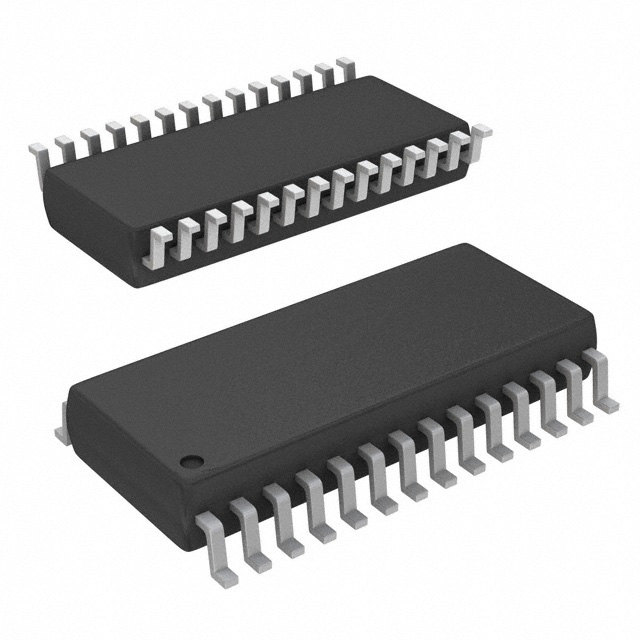
deselected. The CY6264 is packaged in a 450-mil (300-mil body)
SOIC.
■
High speed
❐ 55 ns
■
CMOS for optimum speed/power
■
Easy memory expansion with CE1, CE2 and OE features
■
TTL-compatible inputs and outputs
■
Automatic power-down when deselected
■
Available in Pb-free 28-pin SNC package
An active LOW write enable signal (WE) controls the
writing/reading operation of the memory. When CE1 and WE
inputs are both LOW and CE2 is HIGH, data on the eight data
input/output pins (I/O0 through I/O7) is written into the memory
location addressed by the address present on the address pins
(A0 through A12). Reading the device is accomplished by
selecting the device and enabling the outputs, CE1 and OE
active LOW, CE2 active HIGH, while WE remains inactive or
HIGH. Under these conditions, the contents of the location
addressed by the information on address pins is present on the
eight data input/output pins.
The input/output pins remain in a high-impedance state unless
the chip is selected, outputs are enabled, and write enable (WE)
is HIGH. A die coat is used to ensure alpha immunity.
For a complete list of related documentation, click here.
Logic Block Diagram
Cypress Semiconductor Corporation
Document Number: 001-02367 Rev. *G
•
198 Champion Court
•
San Jose, CA 95134-1709
•
408-943-2600
Revised October 17, 2016
�CY6264
Contents
Pin Configuration ............................................................. 3
Selection Guide ................................................................ 3
Maximum Ratings ............................................................. 4
Operating Range ............................................................... 4
Electrical Characteristics ................................................. 4
Capacitance ...................................................................... 5
AC Test Loads and Waveforms ....................................... 5
Switching Characteristics ................................................ 6
Switching Waveforms ...................................................... 7
Typical DC and AC Characteristics .............................. 10
Truth Table ...................................................................... 11
Address Designators ..................................................... 11
Ordering Information ...................................................... 12
Ordering Code Definitions ......................................... 12
Document Number: 001-02367 Rev. *G
Package Diagram ............................................................ 13
Acronyms ........................................................................ 14
Document Conventions ................................................. 14
Units of Measure ....................................................... 14
Document History Page ................................................. 15
Sales, Solutions, and Legal Information ...................... 16
Worldwide Sales and Design Support ....................... 16
Products .................................................................... 16
PSoC®Solutions ....................................................... 16
Cypress Developer Community ................................. 16
Technical Support ..................................................... 16
Page 2 of 16
�CY6264
Pin Configuration
Figure 1. 28-pin SOIC pinout (Top View)
Selection Guide
Description
Range
-55
-70
Unit
55
70
ns
Commercial
100
100
mA
Industrial
260
200
mA
Automotive-A
–
200
mA
Commercial
15
15
mA
Industrial
30
30
mA
Automotive-A
–
30
mA
Maximum access time
Maximum operating current
Maximum CMOS standby current
Document Number: 001-02367 Rev. *G
Page 3 of 16
�CY6264
Maximum Ratings
Output current into outputs (LOW) ............................. 20 mA
Exceeding maximum ratings may shorten the useful life of the
device. User guidelines are not tested.
Storage temperature ................................ –65 C to +150 C
Ambient temperature
with power applied ................................... –55 C to +125 C
Static discharge voltage
(per MIL-STD-883, Method 3015) ......................... > 2001 V
Latch-up current ................................................... > 200 mA
Operating Range
Supply voltage to ground potential [1] ..........–0.5 V to +7.0 V
Range
DC voltage applied to outputs
in high Z state [1] ..........................................–0.5 V to +7.0 V
Ambient Temperature
VCC
0 C to +70 C
5 V 10%
Commercial
DC input voltage [1] ......................................–0.5 V to +7.0 V
Industrial
–40 C to +85 C
Automotive-A
–40 C to +85 C
Electrical Characteristics
Over the Operating Range
Parameter
Description
Test Conditions
-55
-70
Unit
Min
Max
Min
Max
2.4
–
2.4
–
V
–
0.4
–
0.4
V
VOH
Output HIGH voltage
VCC = Min, IOH = –4.0 mA
VOL
Output LOW voltage
VCC = Min, IOL = 8.0 mA
VIH
Input HIGH voltage
2.2
VCC
2.2
VCC
V
VIL
Input LOW voltage[1]
–0.5
0.8
–0.5
0.8
V
IIX
Input leakage current
GND VI VCC
–5
+5
–5
+5
A
IOZ
Output leakage current
GND VI VCC, output disabled
–5
+5
–5
+5
A
ICC
VCC operating supply current
VCC = Max, IOUT = 0 mA Commercial
–
100
–
100
mA
Industrial
–
260
–
200
Automotive-A
–
–
200
Commercial
–
20
–
20
Industrial
–
50
–
40
Automotive-A
–
–
40
Commercial
–
15
–
15
Industrial
–
30
–
30
Automotive-A
–
–
30
ISB1
ISB2
Automatic CE1 power-down
current
Automatic CE1 power-down
current
Max VCC, CE1 VIH,
Min duty cycle =100%
Max VCC,
CE1 VCC – 0.3 V,
VIN VCC – 0.3 V or
VIN 0.3 V
mA
mA
Note
1. Minimum voltage is equal to –3.0 V for pulse durations less than 30 ns.
Document Number: 001-02367 Rev. *G
Page 4 of 16
�CY6264
Capacitance
Parameter [2]
Description
CIN
Input capacitance
COUT
Output capacitance
Test Conditions
TA = 25 C, f = 1 MHz, VCC = 5.0 V
Max
Unit
7
pF
7
pF
AC Test Loads and Waveforms
Figure 2. AC Test Loads and Waveforms
R1 481
5V
OUTPUT
30 pF
INCLUDING
JIG AND
SCOPE
R2
255
(a)
R1 481
5V
OUTPUT
ALL INPUT PULSES
3.0 V
5 pF
INCLUDING
JIG AND
SCOPE
R2
255
GND
10%
90%
90%
10%
5 ns
5 ns
(b)
Equivalent to:
THEVENIN EQUIVALENT
OUTPUT
167
1.73 V
Note
2. Tested initially and after any design or process changes that may affect these parameters.
Document Number: 001-02367 Rev. *G
Page 5 of 16
�CY6264
Switching Characteristics
Over the Operating Range
Parameter [3]
Description
-55
-70
Min
Max
Min
Max
Unit
READ CYCLE
tRC
Read cycle time
55
–
70
–
ns
tAA
Address to data valid
–
55
–
70
ns
tOHA
Data hold from address change
5
5
–
ns
tACE1
CE1 LOW to data valid
–
55
–
70
ns
tACE2
CE2 HIGH to data valid
–
40
–
70
ns
tDOE
OE LOW to data valid
–
25
–
35
ns
tLZOE
OE LOW to low Z
3
5
–
ns
tHZOE
OE HIGH to high
Z[4]
–
20
–
30
ns
tLZCE1
CE1 LOW to low Z[5]
5
–
5
–
ns
tLZCE2
CE2 HIGH to low Z
3
–
5
–
ns
Z[4, 6]
tHZCE
CE1 HIGH to high
CE2 LOW to high Z
–
20
–
30
ns
tPU
CE1 LOW to power-up
0
–
0
–
ns
tPD
–
25
–
30
ns
WRITE CYCLE
CE1
[6, 7]
tWC
Write cycle time
50
–
70
–
ns
tSCE1
CE1 LOW to write end
40
–
60
–
ns
tSCE2
CE2 HIGH to write end
30
–
50
–
ns
tAW
Address setup to write end
40
–
55
–
ns
tHA
Address hold from write end
0
–
0
–
ns
tSA
Address setup to write start
0
–
0
–
ns
tPWE
WE pulse width
25
–
40
–
ns
tSD
Data setup to write end
25
–
35
–
ns
tHD
Data hold from write end
0
–
0
–
ns
–
20
–
30
ns
5
–
5
–
ns
HIGH to power-down
Z[4]
tHZWE
WE LOW to high
tLZWE
WE HIGH to low Z
Notes
3. Test conditions assume signal transition time of 5 ns or less, timing reference levels of 1.5 V, input pulse levels of 0 to 3.0 V, and output loading of the specified IOL/IOH
and 30-pF load capacitance.
4. tHZOE, tHZCE, and tHZWE are specified with CL = 5 pF as in part (b) of AC Test Loads. Transition is measured 500 mV from steady-state voltage.
5. At any temperature and voltage condition, tHZCE is less than tLZCE for any device.
6. The internal write time of the memory is defined by the overlap of CE1 LOW, CE2 HIGH, and WE LOW. Both signals must be LOW to initiate a write and either signal
can terminate a write by going HIGH. The data input setup and hold timing should be referenced to the rising edge of the signal that terminates the write.
7. The minimum write cycle time for Write Cycle No. 3 (WE Controlled, OE LOW) is the sum of tHZWE and tSD.
Document Number: 001-02367 Rev. *G
Page 6 of 16
�CY6264
Switching Waveforms
Figure 3. Read Cycle No. 1 [8, 9]
tRC
ADDRESS
tAA
tOHA
DATA OUT
PREVIOUS DATA VALID
DATA VALID
Figure 4. Read Cycle No. 2 [10, 11]
tRC
CE1
CE2
tACE
OE
OE
DATA OUT
tDOE
tLZOE
HIGH IMPEDANCE
tLZCE
VCC
SUPPLY
CURRENT
tHZOE
tHZCE
HIGH
IMPEDANCE
DATA VALID
tPD
tPU
ICC
50%
50%
ISB
Notes
8. Device is continuously selected. OE, CE = VIL. CE2 = VIH.
9. Address valid prior to or coincident with CE transition LOW.
10. WE is HIGH for read cycle.
11. Data I/O is High Z if OE = VIH, CE1 = VIH, or WE = VIL.
Document Number: 001-02367 Rev. *G
Page 7 of 16
�CY6264
Switching Waveforms (continued)
Figure 5. Write Cycle No. 1 (WE Controlled) [12, 13]
tWC
ADDRESS
tSCE1
CE1
CE2
tSCE2
OE
tAW
WE
tHA
tSA
tPWE
tHD
tSD
DATAIN VALID
DATA IN
tHZWE
DATA I/O
tLZWE
HIGH IMPEDANCE
DATA UNDEFINED
Figure 6. Write Cycle No. 2 (CE Controlled) [12, 13, 14]
tWC
ADDRESS
CE1
tSCE1
tSA
CE2
tAW
tSCE2
tHA
tPWE
WE
tSD
tHD
DATAIN VALID
DATA IN
tHZWE
DATA I/O
DATA UNDEFINED
HIGH IMPEDANCE
Notes
12. Address valid prior to or coincident with CE transition LOW.
13. Data I/O is High Z if OE = VIH, CE1 = VIH, or WE = VIL.
14. If CE goes HIGH simultaneously with WE HIGH, the output remains in a high-impedance state.
Document Number: 001-02367 Rev. *G
Page 8 of 16
�CY6264
Switching Waveforms (continued)
Figure 7. Write Cycle No. 3 (WE Controlled, OE LOW) [15, 16]
tWC
ADDRESS
CE
tAW
WE
tHA
tSA
tSD
DATA I/O
NOTE 17
tHD
DATAIN VALID
tHZWE
tLZWE
Notes
15. If CE goes HIGH simultaneously with WE HIGH, the output remains in a high-impedance state.
16. The minimum write cycle time for Write Cycle No. 3 (WE Controlled, OE LOW) is the sum of tHZWE and tSD.
17. During this period, the I/Os are in output state and input signals should not be applied.
Document Number: 001-02367 Rev. *G
Page 9 of 16
�CY6264
Typical DC and AC Characteristics
ICC
0.8
0.6
0.4
ISB
0.0
4.0
4.5
5.0
5.5
ICC
0.8
0.6
0.4
VCC =5.0 V
VIN =5.0 V
0.2
ISB
0.0
55
6.0
25
NORMALIZED ACCESS TIME
vs. AMBIENT TEMPERATURE
NORMALIZED ACCESS TIME
vs. SUPPLY VOLTAGE
1.6
1.3
NORMALIZED tAA
NORMALIZED t AA
1.4
1.2
TA =25°C
1.0
1.4
1.2
1.0
VCC =5.0 V
0.8
0.9
0.8
4.0
4.5
5.0
5.5
6.0
0.6
55
3.0
30.0
2.5
25.0
2.0
1.5
1.0
25
3.0
4.0
VCC =5.0 V
TA =25°C
60
40
20
0
0.0
1.0
140
5.0
15.0
SUPPLY VOLTAGE(V)
Document Number: 001-02367 Rev. *G
0.0
VCC =4.5 V
TA =25°C
0
200
400
600
800 1000
CAPACITANCE (pF)
3.0
4.0
OUTPUT SINK CURRENT
vs.OUTPUT VOLTAGE
120
100
VCC =5.0 V
TA =25°C
80
60
40
20
0
0.0
125
20.0
10.0
2.0
OUTPUT VOLTAGE (V)
1.0
2.0
3.0
4.0
OUTPUT VOLTAGE (V)
1.25
5.0
0.5
2.0
80
TYPICAL ACCESS TIME CHANGE
vs. OUTPUT LOADING
DELTA tAA (ns)
NORMALIZED I PO
TYPICAL POWER-ON CURRENT
vs. SUPPLY VOLTAGE
1.0
100
AMBIENT TEMPERATURE (°C)
SUPPLY VOLTAGE (V)
0.0
0.0
OUTPUT SOURCE CURRENT
vs. OUTPUT VOLTAGE
AMBIENT TEMPERATURE (°C)
SUPPLY VOLTAGE (V)
1.1
125
OUTPUT SINK CURRENT (mA)
0.2
1.0
120
NORMALIZED I CC
1.0
NORMALIZED SUPPLY CURRENT
vs. AMBIENT TEMPERATURE
OUTPUT SOURCE CURRENT (mA)
1.2
1.2
NORMALIZED ICC, ISB
NORMALIZED ICC, ISB
1.4
NORMALIZED SUPPLY CURRENT
vs. SUPPLY VOLTAGE
NORMALIZED ICC vs. CYCLE TIME
VCC =5.0 V
TA =25°C
VCC =0.5 V
1.00
0.75
0.50
10
20
30
40
CYCLE FREQUENCY (MHz)
Page 10 of 16
�CY6264
Truth Table
CE1
CE2
WE
OE
Input/Output
Mode
H
X
X
X
High Z
Deselect/Power-down
X
L
X
X
High Z
Deselect
L
H
H
L
Data Out
Read
L
H
L
X
Data In
Write
L
H
H
H
High Z
Deselect
Address Designators
Address Name
Address Function
Pin Number
A4
X3
2
A5
X4
3
A6
X5
4
A7
X6
5
A8
X7
6
A9
Y1
7
A10
Y4
8
A11
Y3
9
A12
Y0
10
A0
Y2
21
A1
X0
23
A2
X1
24
A3
X2
25
Document Number: 001-02367 Rev. *G
Page 11 of 16
�CY6264
Ordering Information
Table 1 lists the CY6264 key package features and ordering codes. The table contains only the parts that are currently available. If
you do not see what you are looking for, contact your local sales representative. For more information, visit the Cypress website at
www.cypress.com and see the product summary page at http://www.cypress.com/products.
Table 1. Static RAM Key Features and Ordering Information
Speed
(ns)
55
Package
Diagram
Ordering Code
CY6264-55SNXI
Package Type
51-85092 28-pin SNC (300 Mils) Narrow Body (Pb-free)
Operating
Range
Industrial
Ordering Code Definitions
CY 62 64 - 55
SN
X
I
Temperature Range:
I = Industrial = –40 °C to +85 °C
Pb-free
Package Type:
SN = 28-pin SNC
Speed: 55 ns
Density: 64-Kbit
Family Code: MoBL SRAM family
Company ID: CY = Cypress
Document Number: 001-02367 Rev. *G
Page 12 of 16
�CY6264
Package Diagram
Figure 8. 28-pin SNC (300 Mils) SN28.3 (Narrow Body) Package Outline, 51-85092
51-85092 *E
Document Number: 001-02367 Rev. *G
Page 13 of 16
�CY6264
Acronyms
Acronym
Document Conventions
Description
Units of Measure
CMOS
Complementary Metal Oxide Semiconductor
I/O
Input/Output
°C
degrees Celsius
SRAM
Static Random Access Memory
MHz
megahertz
TSOP
Thin Small Outline Package
A
microampere
VFBGA
Very Fine-Pitch Ball Grid Array
mA
milliampere
ns
nanosecond
ohm
pF
picofarad
V
volt
W
watt
Document Number: 001-02367 Rev. *G
Symbol
Unit of Measure
Page 14 of 16
�CY6264
Document History Page
Document Title: CY6264, 8K × 8 Static RAM
Document Number: 001-02367
Revision
ECN
Orig. of
Change
Submission
date
**
384870
PCI
06/28/05
Spec # change from 38-00425 to 001-02367
*A
488954
VKN
See ECN
Added Automotive temperature range related information in all instances
across the document.
Updated Electrical Characteristics:
Changed description of IIX parameter from “Input Load Current” to “Input
Leakage Current”.
Removed IOS parameter and its details.
Updated Ordering Information:
Updated part numbers.
Replaced “28-pin SOIC” with “28-pin SNC” in “Package Type” column.
*B
2892510
VKN
See ECN
Updated Ordering Information.
Updated Package Diagram.
Added Sales, Solutions, and Legal Information.
*C
3329873
RAME
07/27/11
Removed “AN1064 - SRAM System Design Guidelines” related information in
all instances across the document.
Added Ordering Code Definitions under Ordering Information.
Added Acronyms, and Units of Measure.
Updated to new template.
*D
4122787
VINI
09/13/2013
Updated Package Diagram:
spec 51-85092 – Changed revision from *C to *E.
Updated to new template.
Completing Sunset Review.
*E
4525875
VINI
10/06/2014
Updated Maximum Ratings:
Referred Note 1 in “Supply voltage to ground potential”.
Updated Switching Characteristics:
Added Note 7 and referred the same note in “WRITE CYCLE”.
Updated Switching Waveforms:
Added Figure 7.
Added Note 15, 16, 17 and referred the same notes in Figure 7.
Completing Sunset Review.
*F
4576406
VINI
01/16/2015
Updated Functional Description:
Added “For a complete list of related documentation, click here.” at the end.
Updated Ordering Information:
Updated part numbers.
*G
5478038
VINI
10/17/2016
Updated Ordering Information:
Updated part numbers.
Updated to new template.
Completing Sunset Review.
Document Number: 001-02367 Rev. *G
Description of Change
Page 15 of 16
�CY6264
Sales, Solutions, and Legal Information
Worldwide Sales and Design Support
Cypress maintains a worldwide network of offices, solution centers, manufacturer’s representatives, and distributors. To find the office
closest to you, visit us at Cypress Locations.
PSoC®Solutions
Products
ARM® Cortex® Microcontrollers
Automotive
cypress.com/arm
cypress.com/automotive
Clocks & Buffers
Interface
cypress.com/clocks
cypress.com/interface
Internet of Things
Lighting & Power Control
Memory
cypress.com/iot
cypress.com/powerpsoc
Cypress Developer Community
Forums | Projects | Video | Blogs | Training | Components
Technical Support
cypress.com/support
cypress.com/memory
PSoC
cypress.com/psoc
Touch Sensing
cypress.com/touch
USB Controllers
Wireless/RF
PSoC 1 | PSoC 3 | PSoC 4 | PSoC 5LP
cypress.com/usb
cypress.com/wireless
© Cypress Semiconductor Corporation, 2005-2016. This document is the property of Cypress Semiconductor Corporation and its subsidiaries, including Spansion LLC ("Cypress"). This document,
including any software or firmware included or referenced in this document ("Software"), is owned by Cypress under the intellectual property laws and treaties of the United States and other countries
worldwide. Cypress reserves all rights under such laws and treaties and does not, except as specifically stated in this paragraph, grant any license under its patents, copyrights, trademarks, or other
intellectual property rights. If the Software is not accompanied by a license agreement and you do not otherwise have a written agreement with Cypress governing the use of the Software, then Cypress
hereby grants you a personal, non-exclusive, nontransferable license (without the right to sublicense) (1) under its copyright rights in the Software (a) for Software provided in source code form, to
modify and reproduce the Software solely for use with Cypress hardware products, only internally within your organization, and (b) to distribute the Software in binary code form externally to end users
(either directly or indirectly through resellers and distributors), solely for use on Cypress hardware product units, and (2) under those claims of Cypress's patents that are infringed by the Software (as
provided by Cypress, unmodified) to make, use, distribute, and import the Software solely for use with Cypress hardware products. Any other use, reproduction, modification, translation, or compilation
of the Software is prohibited.
TO THE EXTENT PERMITTED BY APPLICABLE LAW, CYPRESS MAKES NO WARRANTY OF ANY KIND, EXPRESS OR IMPLIED, WITH REGARD TO THIS DOCUMENT OR ANY SOFTWARE
OR ACCOMPANYING HARDWARE, INCLUDING, BUT NOT LIMITED TO, THE IMPLIED WARRANTIES OF MERCHANTABILITY AND FITNESS FOR A PARTICULAR PURPOSE. To the extent
permitted by applicable law, Cypress reserves the right to make changes to this document without further notice. Cypress does not assume any liability arising out of the application or use of any
product or circuit described in this document. Any information provided in this document, including any sample design information or programming code, is provided only for reference purposes. It is
the responsibility of the user of this document to properly design, program, and test the functionality and safety of any application made of this information and any resulting product. Cypress products
are not designed, intended, or authorized for use as critical components in systems designed or intended for the operation of weapons, weapons systems, nuclear installations, life-support devices or
systems, other medical devices or systems (including resuscitation equipment and surgical implants), pollution control or hazardous substances management, or other uses where the failure of the
device or system could cause personal injury, death, or property damage ("Unintended Uses"). A critical component is any component of a device or system whose failure to perform can be reasonably
expected to cause the failure of the device or system, or to affect its safety or effectiveness. Cypress is not liable, in whole or in part, and you shall and hereby do release Cypress from any claim,
damage, or other liability arising from or related to all Unintended Uses of Cypress products. You shall indemnify and hold Cypress harmless from and against all claims, costs, damages, and other
liabilities, including claims for personal injury or death, arising from or related to any Unintended Uses of Cypress products.
Cypress, the Cypress logo, Spansion, the Spansion logo, and combinations thereof, WICED, PSoC, CapSense, EZ-USB, F-RAM, and Traveo are trademarks or registered trademarks of Cypress in
the United States and other countries. For a more complete list of Cypress trademarks, visit cypress.com. Other names and brands may be claimed as property of their respective owners.
Document Number: 001-02367 Rev. *G
Revised October 17, 2016
Page 16 of 16
�