CY74FCT2646T
8-BIT REGISTERED TRANSCEIVER
WITH 3-STATE OUTPUTS
SCCS043C – SEPTEMBER 1994 – REVISED NOVEMBER 2001
D
D
D
D
D
D
D
D
D
D
D
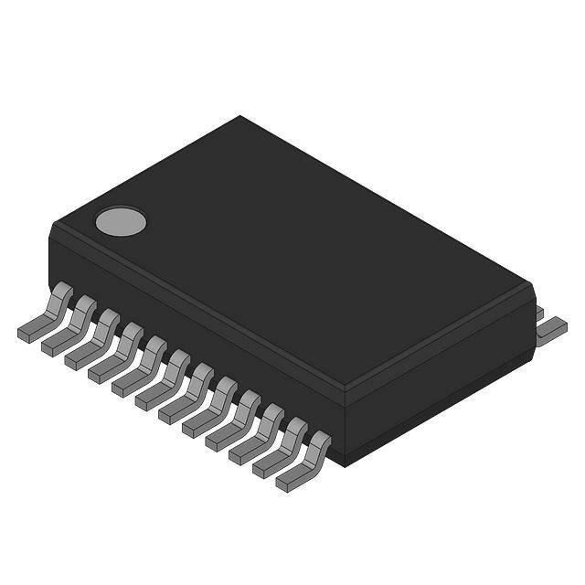
Q PACKAGE
(TOP VIEW)
Function and Pinout Compatible With FCT
and F Logic
Reduced VOH (Typically = 3.3 V) Versions
of Equivalent FCT Functions
25-Ω Output Series Resistors to Reduce
Transmission-Line Reflection Noise
Edge-Rate Control Circuitry for
Significantly Improved Noise
Characteristics
Ioff Supports Partial-Power-Down Mode
Operation
Matched Rise and Fall Times
ESD Protection Exceeds JESD 22
– 2000-V Human-Body Model (A114-A)
– 200-V Machine Model (A115-A)
– 1000-V Charged-Device Model (C101)
Fully Compatible With TTL Input and
Output Logic Levels
12-mA Output Sink Current
15-mA Output Source Current
Independent Register for A and B Buses
3-State Outputs
CPAB
SAB
DIR
A1
A2
A3
A4
A5
A6
A7
A8
GND
1
24
2
23
3
22
4
21
5
20
6
19
7
18
8
17
9
16
10
15
11
14
12
13
VCC
CPBA
SBA
G
B1
B2
B3
B4
B5
B6
B7
B8
description
The CY74FCT2646T consists of a bus transceiver circuit with 3-state, D-type flip-flops, and control circuitry
arranged for multiplexed transmission of data directly from the input bus or from the internal registers. Data on
the A or B bus is clocked into the registers as the appropriate clock pin goes to a high logic level.
Output-enable (G) and direction-control (DIR) inputs determine the transceiver function. On-chip termination
resistors at the outputs reduce system noise caused by reflections, so that the CY74FCT2646T can replace
the CY74FCT646T in an existing design.
In the transceiver mode, data present at the high-impedance port can be stored in either the A or B register,
or in both. Select controls (SAB, SBA) can multiplex stored and real-time (transparent mode) data. DIR
determines which bus receives data when G is active low. In the isolation mode (G is high), A data can be stored
in the B register and/or B data can be stored in the A register.
This device is fully specified for partial-power-down applications using Ioff. The Ioff circuitry disables the outputs,
preventing damaging current backflow through the device when it is powered down.
PIN DESCRIPTION
DESCRIPTION
NAME
A
Data register A inputs, data register B outputs
B
Data register B inputs, data register A outputs
CPAB, CPBA
SAB, SBA
DIR, G
Clock pulse inputs
Output data source select inputs
Output-enable inputs
Please be aware that an important notice concerning availability, standard warranty, and use in critical applications of
Texas Instruments semiconductor products and disclaimers thereto appears at the end of this data sheet.
Copyright 2001, Texas Instruments Incorporated
PRODUCTION DATA information is current as of publication date.
Products conform to specifications per the terms of Texas Instruments
standard warranty. Production processing does not necessarily include
testing of all parameters.
POST OFFICE BOX 655303
• DALLAS, TEXAS 75265
1
�CY74FCT2646T
8-BIT REGISTERED TRANSCEIVER
WITH 3-STATE OUTPUTS
SCCS043C – SEPTEMBER 1994 – REVISED NOVEMBER 2001
ORDERING INFORMATION
SPEED
(ns)
PACKAGE†
TA
–40°C
40°C to 85°C
QSOP – Q
Tape and reel
ORDERABLE
PART NUMBER
5.4
CY74FCT2646CTQCT
TOP-SIDE
MARKING
FCT2646C
QSOP – Q Tape and reel
6.3
CY74FCT2646ATQCT
FCT2646A
† Package drawings, standard packing quantities, thermal data, symbolization, and PCB design guidelines
are available at www.ti.com/sc/package.
FUNCTION TABLE
DATA I/O‡
INPUTS
OPERATION OR
FUNCTION
G
DIR
CPAB
CPBA
SAB
SBA
A1–A8
B1–B8
H
X
H or L
H or L
X
X
Input
Input
H
X
↑
↑
X
X
Input
Input
Store A and B data
L
L
X
X
X
L
Output
Input
Real-time B data to A bus
L
L
X
H or L
X
H
Output
Input
Stored B data to A bus
L
H
X
X
L
X
Input
Output
Real-time A data to B bus
L
H
H or L
X
H
X
Input
Output
Stored A data to B bus
Isolation
H = High logic level, L = Low logic level, X = Don’t care, ↑ = Low-to-high clock transition
‡ The data output functions can be enabled or disabled by various signals at the G or DIR inputs. Data input
functions always are enabled, i.e., data at the bus pins is stored on every low-to-high transition of the clock
inputs.
2
POST OFFICE BOX 655303
• DALLAS, TEXAS 75265
�CY74FCT2646T
8-BIT REGISTERED TRANSCEIVER
WITH 3-STATE OUTPUTS
3
DIR
L
21
G
L
1
CPAB
X
23
CPBA
X
2
SAB
X
BUS B
BUS A
BUS A
BUS B
SCCS043C – SEPTEMBER 1994 – REVISED NOVEMBER 2001
22
SBA
X
3
DIR
H
21
G
L
21
1
G
L
L
H
CPAB
↑
X
↑
23
CPBA
X
↑
↑
2
SAB
L
22
SBA
X
BUS B
BUS A
BUS A
3
DIR
H
L
X
23
CPBA
X
REAL-TIME TRANSFER
BUS A TO BUS B
BUS B
REAL-TIME TRANSFER
BUS B TO BUS A
1
CPAB
X
2
22
3
21
1
23
2
22
SAB
SBA
CPBA
SAB
SBA
X
X
X
G
L
L
CPAB
X
X
X
DIR†
L
H
X
H or L
H or L
X
X
H
H
H
STORAGE FROM
A AND/OR B
TRANSFER STORED DATA
TO A AND/OR B
† Cannot transfer data to A bus and B bus simultaneously.
Figure 1. Bus-Management Functions
POST OFFICE BOX 655303
• DALLAS, TEXAS 75265
3
�CY74FCT2646T
8-BIT REGISTERED TRANSCEIVER
WITH 3-STATE OUTPUTS
SCCS043C – SEPTEMBER 1994 – REVISED NOVEMBER 2001
logic diagram
G
DIR
CPBA
SBA
CPAB
SAB
21
3
23
22
1
2
D
C
A1
4
20
B1
D
C
To Seven Other Channels
absolute maximum ratings over operating free-air temperature range (unless otherwise noted)†
Supply voltage range to ground potential . . . . . . . . . . . . . . . . . . . . . . . . . . . . . . . . . . . . . . . . . . . . . . –0.5 V to 7 V
DC input voltage range . . . . . . . . . . . . . . . . . . . . . . . . . . . . . . . . . . . . . . . . . . . . . . . . . . . . . . . . . . . . . –0.5 V to 7 V
DC output voltage range . . . . . . . . . . . . . . . . . . . . . . . . . . . . . . . . . . . . . . . . . . . . . . . . . . . . . . . . . . . . –0.5 V to 7 V
DC output current (maximum sink current/pin) . . . . . . . . . . . . . . . . . . . . . . . . . . . . . . . . . . . . . . . . . . . . . . 120 mA
Package thermal impedance, θJA (see Note 1) . . . . . . . . . . . . . . . . . . . . . . . . . . . . . . . . . . . . . . . . . . . . . 61°C/W
Ambient temperature range with power applied, TA . . . . . . . . . . . . . . . . . . . . . . . . . . . . . . . . . . . –65°C to 135°C
Storage temperature range, Tstg . . . . . . . . . . . . . . . . . . . . . . . . . . . . . . . . . . . . . . . . . . . . . . . . . . . –65°C to 150°C
† Stresses beyond those listed under “absolute maximum ratings” may cause permanent damage to the device. These are stress ratings only, and
functional operation of the device at these or any other conditions beyond those indicated under “recommended operating conditions” is not implied.
Exposure to absolute-maximum-rated conditions for extended periods may affect device reliability.
NOTE 1: The package thermal impedance is calculated in accordance with JESD 51-7.
4
POST OFFICE BOX 655303
• DALLAS, TEXAS 75265
�CY74FCT2646T
8-BIT REGISTERED TRANSCEIVER
WITH 3-STATE OUTPUTS
SCCS043C – SEPTEMBER 1994 – REVISED NOVEMBER 2001
recommended operating conditions (see Note 2)
MIN
NOM
MAX
UNIT
4.75
5
5.25
V
VCC
VIH
Supply voltage
VIL
IOH
Low-level input voltage
0.8
V
High-level output current
–15
mA
IOL
TA
Low-level output current
12
mA
85
°C
High-level input voltage
2
Operating free-air temperature
–40
V
NOTE 2: All unused inputs of the device must be held at VCC or GND to ensure proper device operation.
POST OFFICE BOX 655303
• DALLAS, TEXAS 75265
5
�CY74FCT2646T
8-BIT REGISTERED TRANSCEIVER
WITH 3-STATE OUTPUTS
SCCS043C – SEPTEMBER 1994 – REVISED NOVEMBER 2001
electrical characteristics over recommended operating free-air temperature range (unless
otherwise noted)
PARAMETER
TEST CONDITIONS
VIK
VOH
VCC = 4.75,
VCC = 4.75,
IIN = –18 mA
IOH = –15 mA
VOL
Rout
VCC = 4.75,
VCC = 4.75,
IOL = 12 mA
IOL = 12 mA
Vhys
All inputs
MIN
2.4
20
TYP†
MAX
UNIT
–0.7
–1.2
V
3.3
V
0.3
0.55
V
25
40
Ω
0.2
V
25 V
VCC = 5
5.25
VIN = VCC
VIN = 2.7 V
±1
IIL
IOZH
IOZL
IOS‡
VCC = 5.25 V,
VCC = 5.25 V,
VIN = 0.5 V
VOUT = 2.7 V
±1
µA
10
µA
VCC = 5.25 V,
VCC = 5.25 V,
VOUT = 0.5 V
VOUT = 0 V
Ioff
ICC
VCC = 0 V,
VCC = 5.25 V,
IIH
∆ICC
ICCD¶
IC#
5
–10
µA
–225
mA
±1
µA
0.1
0.2
mA
0.5
2
mA
0.06
0.12
mA/
MHz
0.7
1.4
VIN = 3.4 V or GND
VIN ≤ 0.2 V or
VIN ≥ VCC – 0.2 V
1.2
3.4
2.8
5.6||
VIN = 3.4 V or GND
5.1
14.6||
6
10
–60
VOUT = 4.5 V
VIN ≤ 0.2 V,
VIN ≥ VCC – 0.2 V
VCC = 5.25 V, VIN = 3.4 V§, f1 = 0, Outputs open
VCC = 5.25 V, One input switching at 50% duty cycle, Outputs open,
G = DIR = GND, GAB = GBA = GND, VIN ≤ 0.2 V or VIN ≥ VCC – 0.2 V
25 V
VCC = 5
5.25
V,
Outputs open,,
G = DIR = GND,
GAB = GBA = GND
One input switching
at f1 = 5 MHz
at 50% duty cycle
Eight bits switching
at f1 = 5 MHz
at 50% duty cycle
µA
VIN ≤ 0.2 V or
VIN ≥ VCC – 0.2 V
Ci
–120
mA
pF
Co
8
12
pF
† Typical values are at VCC = 5 V, TA = 25°C.
‡ Not more than one output should be shorted at a time. Duration of short should not exceed one second. The use of high-speed test apparatus and/or
sample-and-hold techniques are preferable to minimize internal chip heating and more accurately reflect operational values. Otherwise, prolonged
shorting of a high output can raise the chip temperature well above normal and cause invalid readings in other parametric tests. In any sequence
of parameter tests, IOS tests should be performed last.
§ Per TTL-driven input (VIN = 3.4 V); all other inputs at VCC or GND
¶ This parameter is derived for use in total power-supply calculations.
# IC
= ICC + ∆ICC × DH × NT + ICCD (f0/2 + f1 × N1)
Where:
IC
= Total supply current
ICC = Power-supply current with CMOS input levels
∆ICC = Power-supply current for a TTL high input (VIN = 3.4 V)
DH
= Duty cycle for TTL inputs high
NT
= Number of TTL inputs at DH
ICCD = Dynamic current caused by an input transition pair (HLH or LHL)
f0
= Clock frequency for registered devices, otherwise zero
f1
= Input signal frequency
N1
= Number of inputs changing at f1
All currents are in milliamperes and all frequencies are in megahertz.
|| Values for these conditions are examples of the ICC formula.
6
POST OFFICE BOX 655303
• DALLAS, TEXAS 75265
�CY74FCT2646T
8-BIT REGISTERED TRANSCEIVER
WITH 3-STATE OUTPUTS
SCCS043C – SEPTEMBER 1994 – REVISED NOVEMBER 2001
timing requirements over recommended operating free-air temperature range (unless otherwise
noted) (see Figure 2)
CY74FCT2646AT
MIN
tw
tsu
Pulse duration, high or low
Setup time, high or low
Data before CPBA↑ or CPAB↑
th
Hold time, high or low
Data after CPBA↑ or CPAB↑
MAX
CY74FCT2646CT
MIN
MAX
UNIT
5
5
ns
2
2
ns
1.5
1.5
ns
switching characteristics over operating free-air temperature range (see Figure 2)
PARAMETER
FROM
(INPUT)
TO
(OUTPUT)
tPLH
tPHL
A or B
B or A
tPZH
tPZL
G
A or B
tPZH
tPZL
DIR
A or B
tPHZ
tPLZ
G
A or B
tPHZ
tPLZ
DIR
A or B
tPLH
tPHL
CPAB or CPBA
B or A
tPLH
tPHL
SAB or SBA
B or A
POST OFFICE BOX 655303
CY74FCT2646AT
• DALLAS, TEXAS 75265
CY74FCT2646CT
MIN
MAX
MIN
MAX
1.5
6.3
1.5
5.4
1.5
6.3
1.5
5.4
1.5
9.8
1.5
7.8
1.5
9.8
1.5
7.8
1.5
9.8
1.5
7.8
1.5
9.8
1.5
7.8
1.5
6.3
1.5
6.3
1.5
6.3
1.5
6.3
1.5
6.3
1.5
6.3
1.5
6.3
1.5
6.3
1.5
6.3
1.5
5.7
1.5
6.3
1.5
5.7
1.5
7.7
1.5
6.2
1.5
7.7
1.5
6.2
UNIT
ns
ns
ns
ns
ns
ns
ns
7
�CY74FCT2646T
8-BIT REGISTERED TRANSCEIVER
WITH 3-STATE OUTPUTS
SCCS043C – SEPTEMBER 1994 – REVISED NOVEMBER 2001
PARAMETER MEASUREMENT INFORMATION
7V
From Output
Under Test
From Output
Under Test
Test
Point
CL = 50 pF
(see Note A)
Open
TEST
GND
CL = 50 pF
(see Note A)
500 Ω
S1
500 Ω
S1
Open
7V
Open
tPLH/tPHL
tPLZ/tPZL
tPHZ/tPZH
500 Ω
LOAD CIRCUIT FOR
3-STATE OUTPUTS
LOAD CIRCUIT FOR
TOTEM-POLE OUTPUTS
3V
1.5 V
Timing Input
0V
tw
tsu
3V
1.5 V
Input
1.5 V
th
3V
1.5 V
Data Input
1.5 V
0V
0V
VOLTAGE WAVEFORMS
PULSE DURATION
VOLTAGE WAVEFORMS
SETUP AND HOLD TIMES
3V
1.5 V
Input
1.5 V
0V
tPLH
tPHL
1.5 V
1.5 V
VOL
tPHL
Out-of-Phase
Output
tPLZ
≈3.5 V
1.5 V
tPZH
VOH
1.5 V
VOL
1.5 V
0V
Output
Waveform 1
(see Note B)
tPLH
1.5 V
1.5 V
tPZL
VOH
In-Phase
Output
3V
Output
Control
Output
Waveform 2
(see Note B)
VOLTAGE WAVEFORMS
PROPAGATION DELAY TIMES
INVERTING AND NONINVERTING OUTPUTS
VOL + 0.3 V
VOL
tPHZ
1.5 V
VOH – 0.3 V
VOH
≈0 V
VOLTAGE WAVEFORMS
ENABLE AND DISABLE TIMES
LOW- AND HIGH-LEVEL ENABLING
NOTES: A. CL includes probe and jig capacitance.
B. Waveform 1 is for an output with internal conditions such that the output is low except when disabled by the output control.
Waveform 2 is for an output with internal conditions such that the output is high except when disabled by the output control.
C. The outputs are measured one at a time with one input transition per measurement.
Figure 2. Load Circuit and Voltage Waveforms
8
POST OFFICE BOX 655303
• DALLAS, TEXAS 75265
�PACKAGE OPTION ADDENDUM
www.ti.com
11-Nov-2009
PACKAGING INFORMATION
Orderable Device
Status (1)
Package
Type
Package
Drawing
Pins Package Eco Plan (2)
Qty
74FCT2646ATQCTE4
ACTIVE
SSOP/
QSOP
DBQ
24
2500 Green (RoHS &
no Sb/Br)
CU NIPDAU
Level-2-260C-1 YEAR
CY74FCT2646ATQCT
ACTIVE
SSOP/
QSOP
DBQ
24
2500 Green (RoHS &
no Sb/Br)
CU NIPDAU
Level-2-260C-1 YEAR
SN74FCT2646ATQCTG4
ACTIVE
SSOP/
QSOP
DBQ
24
2500 Green (RoHS &
no Sb/Br)
CU NIPDAU
Level-2-260C-1 YEAR
Lead/Ball Finish
MSL Peak Temp (3)
(1)
The marketing status values are defined as follows:
ACTIVE: Product device recommended for new designs.
LIFEBUY: TI has announced that the device will be discontinued, and a lifetime-buy period is in effect.
NRND: Not recommended for new designs. Device is in production to support existing customers, but TI does not recommend using this part in
a new design.
PREVIEW: Device has been announced but is not in production. Samples may or may not be available.
OBSOLETE: TI has discontinued the production of the device.
(2)
Eco Plan - The planned eco-friendly classification: Pb-Free (RoHS), Pb-Free (RoHS Exempt), or Green (RoHS & no Sb/Br) - please check
http://www.ti.com/productcontent for the latest availability information and additional product content details.
TBD: The Pb-Free/Green conversion plan has not been defined.
Pb-Free (RoHS): TI's terms "Lead-Free" or "Pb-Free" mean semiconductor products that are compatible with the current RoHS requirements
for all 6 substances, including the requirement that lead not exceed 0.1% by weight in homogeneous materials. Where designed to be soldered
at high temperatures, TI Pb-Free products are suitable for use in specified lead-free processes.
Pb-Free (RoHS Exempt): This component has a RoHS exemption for either 1) lead-based flip-chip solder bumps used between the die and
package, or 2) lead-based die adhesive used between the die and leadframe. The component is otherwise considered Pb-Free (RoHS
compatible) as defined above.
Green (RoHS & no Sb/Br): TI defines "Green" to mean Pb-Free (RoHS compatible), and free of Bromine (Br) and Antimony (Sb) based flame
retardants (Br or Sb do not exceed 0.1% by weight in homogeneous material)
(3)
MSL, Peak Temp. -- The Moisture Sensitivity Level rating according to the JEDEC industry standard classifications, and peak solder
temperature.
Important Information and Disclaimer:The information provided on this page represents TI's knowledge and belief as of the date that it is
provided. TI bases its knowledge and belief on information provided by third parties, and makes no representation or warranty as to the
accuracy of such information. Efforts are underway to better integrate information from third parties. TI has taken and continues to take
reasonable steps to provide representative and accurate information but may not have conducted destructive testing or chemical analysis on
incoming materials and chemicals. TI and TI suppliers consider certain information to be proprietary, and thus CAS numbers and other limited
information may not be available for release.
In no event shall TI's liability arising out of such information exceed the total purchase price of the TI part(s) at issue in this document sold by TI
to Customer on an annual basis.
Addendum-Page 1
�PACKAGE MATERIALS INFORMATION
www.ti.com
29-Jul-2009
TAPE AND REEL INFORMATION
*All dimensions are nominal
Device
CY74FCT2646ATQCT
Package Package Pins
Type Drawing
SSOP/
QSOP
DBQ
24
SPQ
Reel
Reel
A0
Diameter Width (mm)
(mm) W1 (mm)
2500
330.0
16.4
Pack Materials-Page 1
6.5
B0
(mm)
K0
(mm)
P1
(mm)
9.0
2.1
8.0
W
Pin1
(mm) Quadrant
16.0
Q1
�PACKAGE MATERIALS INFORMATION
www.ti.com
29-Jul-2009
*All dimensions are nominal
Device
Package Type
Package Drawing
Pins
SPQ
Length (mm)
Width (mm)
Height (mm)
CY74FCT2646ATQCT
SSOP/QSOP
DBQ
24
2500
346.0
346.0
33.0
Pack Materials-Page 2
���IMPORTANT NOTICE
Texas Instruments Incorporated and its subsidiaries (TI) reserve the right to make corrections, modifications, enhancements, improvements,
and other changes to its products and services at any time and to discontinue any product or service without notice. Customers should
obtain the latest relevant information before placing orders and should verify that such information is current and complete. All products are
sold subject to TI’s terms and conditions of sale supplied at the time of order acknowledgment.
TI warrants performance of its hardware products to the specifications applicable at the time of sale in accordance with TI’s standard
warranty. Testing and other quality control techniques are used to the extent TI deems necessary to support this warranty. Except where
mandated by government requirements, testing of all parameters of each product is not necessarily performed.
TI assumes no liability for applications assistance or customer product design. Customers are responsible for their products and
applications using TI components. To minimize the risks associated with customer products and applications, customers should provide
adequate design and operating safeguards.
TI does not warrant or represent that any license, either express or implied, is granted under any TI patent right, copyright, mask work right,
or other TI intellectual property right relating to any combination, machine, or process in which TI products or services are used. Information
published by TI regarding third-party products or services does not constitute a license from TI to use such products or services or a
warranty or endorsement thereof. Use of such information may require a license from a third party under the patents or other intellectual
property of the third party, or a license from TI under the patents or other intellectual property of TI.
Reproduction of TI information in TI data books or data sheets is permissible only if reproduction is without alteration and is accompanied
by all associated warranties, conditions, limitations, and notices. Reproduction of this information with alteration is an unfair and deceptive
business practice. TI is not responsible or liable for such altered documentation. Information of third parties may be subject to additional
restrictions.
Resale of TI products or services with statements different from or beyond the parameters stated by TI for that product or service voids all
express and any implied warranties for the associated TI product or service and is an unfair and deceptive business practice. TI is not
responsible or liable for any such statements.
TI products are not authorized for use in safety-critical applications (such as life support) where a failure of the TI product would reasonably
be expected to cause severe personal injury or death, unless officers of the parties have executed an agreement specifically governing
such use. Buyers represent that they have all necessary expertise in the safety and regulatory ramifications of their applications, and
acknowledge and agree that they are solely responsible for all legal, regulatory and safety-related requirements concerning their products
and any use of TI products in such safety-critical applications, notwithstanding any applications-related information or support that may be
provided by TI. Further, Buyers must fully indemnify TI and its representatives against any damages arising out of the use of TI products in
such safety-critical applications.
TI products are neither designed nor intended for use in military/aerospace applications or environments unless the TI products are
specifically designated by TI as military-grade or "enhanced plastic." Only products designated by TI as military-grade meet military
specifications. Buyers acknowledge and agree that any such use of TI products which TI has not designated as military-grade is solely at
the Buyer's risk, and that they are solely responsible for compliance with all legal and regulatory requirements in connection with such use.
TI products are neither designed nor intended for use in automotive applications or environments unless the specific TI products are
designated by TI as compliant with ISO/TS 16949 requirements. Buyers acknowledge and agree that, if they use any non-designated
products in automotive applications, TI will not be responsible for any failure to meet such requirements.
Following are URLs where you can obtain information on other Texas Instruments products and application solutions:
Products
Applications
Amplifiers
amplifier.ti.com
Audio
www.ti.com/audio
Data Converters
dataconverter.ti.com
Automotive
www.ti.com/automotive
DLP® Products
www.dlp.com
Communications and
Telecom
www.ti.com/communications
DSP
dsp.ti.com
Computers and
Peripherals
www.ti.com/computers
Clocks and Timers
www.ti.com/clocks
Consumer Electronics
www.ti.com/consumer-apps
Interface
interface.ti.com
Energy
www.ti.com/energy
Logic
logic.ti.com
Industrial
www.ti.com/industrial
Power Mgmt
power.ti.com
Medical
www.ti.com/medical
Microcontrollers
microcontroller.ti.com
Security
www.ti.com/security
RFID
www.ti-rfid.com
Space, Avionics &
Defense
www.ti.com/space-avionics-defense
RF/IF and ZigBee® Solutions www.ti.com/lprf
Video and Imaging
www.ti.com/video
Wireless
www.ti.com/wireless-apps
Mailing Address: Texas Instruments, Post Office Box 655303, Dallas, Texas 75265
Copyright © 2010, Texas Instruments Incorporated
�