1CY 7B9 51
CY7B951
Local Area Network ATM Transceiver
Features
• SONET/SDH and ATM Compatible • Compatible with PMC-Sierra PM5345 SUNI™ • Clock and data recovery from 51.84- or 155.52-MHz datastream • 155.52-MHz clock multiplication from 19.44-MHz source • 51.84-MHz clock multiplication from 6.48-MHz source • ±1% frequency agility • Line Receiver Inputs: No external buffering required • Differential output buffering • 100K ECL compatible I/O • No output clock “drift” without data transitions • Link Status Indication • Loop-back testing • Single +5V supply • 24-pin SOIC • Compatible with fiber-optic modules, coaxial cable, and twisted pair media • No external PLL components • Power-down options to minimize power or crosstalk • Low operating current: 0°C VCC − 1.03 VCC − 1.08 VCC − 1.86 0.6 VCC − 0.75 VCC/2 − 0.5 0.0 VCC VCC/2 + 0.5 0.75 VCC − 0.83 VCC − 0.83 VCC − 1.62 V V V V V V V Test Condition Min. 2.0 2.5 2.5 -0.5 VCC − 1.475 0.8 Max. Unit V V V V
Three-Level Input Pins (MODE)
Capacitance[6]
Parameter CIN Description Input Capacitance Test Conditions TA = 25°C, f0 = 1 MHz, VCC = 5.0V Max. 10 Unit pF
Notes: 2. Tested one output at a time, output shorted for less than one second, less than 10% duty cycle. 3. Input currents are always positive at all voltages above VCC/2. 4. Specified only for temperatures below 0°C. 5. Total Receiver operating current (assuming that the Transmitter is not activated) can be found by adding ICCS + ICCR + x * ICCE; where x is 2 if the ROUT± outputs are not activated and 3 if they are activated. Total Transmitter operating current (assuming that the Receiver is not activated) can be found by adding ICCS + ICCT + x * ICCE ; where x is 1 if the TOUT± outputs are not activated and 2 if they are activated. Total device power (assuming that the Transmitter and the Receiver are activated) can be found by adding ICCS + ICCR + ICCT + x * ICCE; where x represents the number of ECL output pairs activated. 6. Tested initially and after any design or process changes that may affect these parameters.
6
�CY7B951
AC Test Loads and Waveforms
5V OUTPUT R1 = 910 Ω R2 = 510 Ω CL < 30 pF (Includes fixture and probe capacitance) R1 CL R2 CL RL VCC − 2
RL = 50 Ω CL < 5 pF (Includes fixture and probe capacitance)
7B951-7
(a) TTL AC Test Load
3.0V 3.0V 2.0V GND < 1 ns 1.0V 2.0V
[7]
(b) ECL AC Test Load [7]
VIHE 80% VILE 20% VILE
VIHE 1.0V < 1 ns
7B951-5
80% 20% < 1 ns
7B951-6
< 1 ns
(c) TTL Input Test Waveform
(d) ECL Input Test Waveform
Switching Characteristics Over the Operating Range
Parameter fREF fB tPE tODC tRF tLOCK tRPWH tRPWL tDV tDH tPD Reference Frequency Bit Time[8] Receiver Static Phase Error[6] Description MODE=LOW MODE=HIGH MODE=LOW MODE=HIGH MODE=LOW MODE=HIGH Output Duty Cycle (TCLK±, RCLK±)[6] Output Rise/Fall Time[6] 25%)[9] 10 10 3 1 TOUT)[10] 10 PLL Lock Time (RIN transition density REFCLK Pulse Width HIGH REFCLK Pulse Width LOW Data Valid Data Hold Propagation Delay (RIN to ROUT, TSER to 48 0.4 Min. 6.41 19.24 19.5 6.50 Max. 6.55 19.64 19.1 6.40 100 200 52 1.2 100 Unit MHz MHz ns ns ps ps % ns µs ns ns ns ns ns
Notes: 7. Cypress uses constant current (ATE) load configurations and forcing functions. This figure is for reference only. 8. fB is calculated as 1/(fREFX8). 9. tLOCK is the time needed for transitioning from lock to REFCLK X8 to lock to data. 10. The ECL switching threshold is the differential zero crossing (i.e., the place where + and − signals cross).
7
�CY7B951
Switching Waveforms for the CY7B951 SONET/SDH Serial Transceiver
tRPWL tRPWH
REFCLK
7B951–8
TSER± (RIN±) tPD TOUT± (ROUT ± )
7B951–9
tODC
tODC
RCLK+ tDV RSER± tDH
7B951–10
tB/2RIN±
tPE
tB/2-
tPE
7B951–11
Ordering Information
Speed (ns) 25 25 Ordering Code CY7B951-SC CY7B951-SI Package Name S13 S13 Package Type 24-Lead (300-Mil) Molded SOIC 24-Lead (300-Mil) Molded SOIC Operating Range Commercial Industrial
Document #: 38-00358-D
8
�CY7B951
Package Diagram
24-Lead (300-Mil) Molded SOIC S13
© Cypress Semiconductor Corporation, 1993. The information contained herein is subject to change without notice. Cypress Semiconductor Corporation assumes no responsibility for the use of any circuitry other than circuitry embodied in a Cypress Semiconductor product. Nor does it convey or imply any license under patent or other rights. Cypress Semiconductor does not authorize its products for use as critical components in life-support systems where a malfunction or failure may reasonably be expected to result in significant injury to the user. The inclusion of Cypress Semiconductor products in life-support systems application implies that the manufacturer assumes all risk of such use and in doing so indemnifies Cypress Semiconductor against all charges.
�
很抱歉,暂时无法提供与“CY7B951-SI”相匹配的价格&库存,您可以联系我们找货
免费人工找货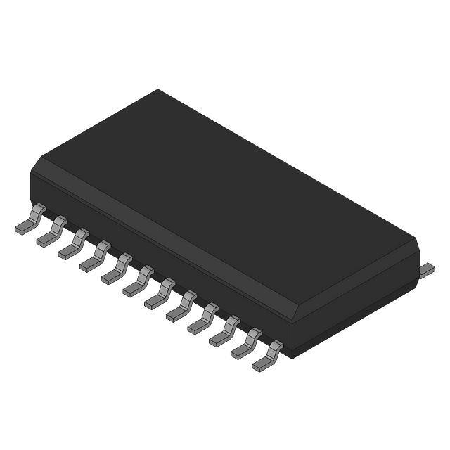


 工商网监
湘ICP备2023018690号
工商网监
湘ICP备2023018690号