CY7B9910
Low Skew Clock Buffer
Low Skew Clock Buffer
Features
The completely integrated PLL enables ‘zero delay’ capability.
External divide capability, combined with the internal PLL, allows
distribution of a low frequency clock that is multiplied by virtually
any factor at the clock destination. This facility minimizes clock
distribution difficulty while allowing maximum system clock
speed and flexibility.
■
All outputs skew < 100 ps typical (250 max)
■
15 MHz to 80 MHz output operation
■
Zero input to output delay
■
50% duty cycle outputs
■
Outputs drive 50 terminated lines
Block Diagram Description
■
Low operating current
Phase Frequency Detector and Filter
■
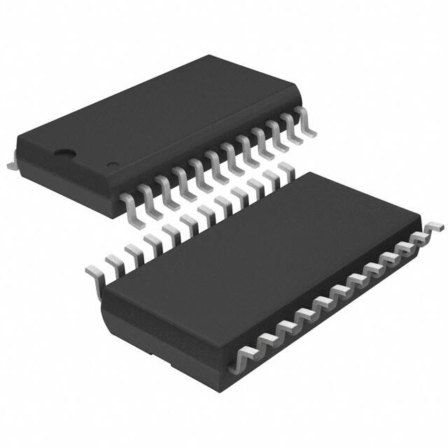
24-pin small-outline integrated circuit (SOIC) package
■
Jitter: < 200 ps peak-to-peak, < 25 ps RMS
The phase frequency detector and Filter blocks accept inputs
from the reference frequency (REF) input and the feedback (FB)
input and generate correction information to control the
frequency of the voltage controlled oscillator (VCO). These
blocks, along with the VCO, form a phase-locked loop (PLL) that
tracks the incoming REF signal.
For a complete list of related documentation, click here.
Functional Description
The CY7B9910 low skew clock buffer offers low skew system
clock distribution. These multiple output clock drivers optimize
the timing of high performance computer systems. Each of the
eight individual drivers can drive terminated transmission lines
with impedances as low as 50 . They deliver minimal and
specified output skews and full swing logic levels (CY7B9910
TTL).
VCO
The VCO accepts analog control inputs from the PLL filter block
and generates a frequency. The operational range of the VCO is
determined by the FS control pin.
Logic Block Diagram
TEST
FB
Phase
Freq Det
Filter
REF
Voltage
Controlled
Oscillator
FS
Q0
Q1
Q2
Q3
Q4
Q5
Q6
Q7
Cypress Semiconductor Corporation
Document Number: 38-07135 Rev. *M
•
198 Champion Court
•
San Jose, CA 95134-1709
•
408-943-2600
Revised November 24, 2017
�CY7B9910
Contents
Pinouts .............................................................................. 3
Pin Definitions .................................................................. 3
Test Mode .......................................................................... 3
Maximum Ratings ............................................................. 4
Operating Range ............................................................... 4
Electrical Characteristics ................................................. 4
Capacitance ...................................................................... 6
Thermal Resistance .......................................................... 6
AC Test Loads and Waveforms ....................................... 6
Switching Characteristics ................................................ 7
AC Timing Diagrams ........................................................ 8
Operational Mode Descriptions ...................................... 9
Ordering Information ...................................................... 10
Ordering Code Definitions ......................................... 10
Document Number: 38-07135 Rev. *M
Package Diagram ............................................................ 11
Acronyms ........................................................................ 12
Document Conventions ................................................. 12
Units of Measure ....................................................... 12
Document History Page ................................................. 13
Sales, Solutions, and Legal Information ...................... 14
Worldwide Sales and Design Support ....................... 14
Products .................................................................... 14
PSoC®Solutions ....................................................... 14
Cypress Developer Community ................................. 14
Technical Support ..................................................... 14
Page 2 of 14
�CY7B9910
Pinouts
Figure 1. 24-pin SOIC pinout
SOIC
Top View
REF
VCCQ
FS
NC
VCCQ
VCCN
Q0
Q1
GND
Q2
Q3
VCCN
1
24
2
23
3
22
4
21
20
5
6
7B9910
19
7
18
8
17
9
16
10
15
11
14
12
13
GND
TEST
NC
GND
VCCN
Q7
Q6
GND
Q5
Q4
VCCN
FB
Pin Definitions
Signal Name
I/O
Description
REF[1]
I
Reference frequency input. This input supplies the frequency and timing against which all functional
variations are measured.
FB
I
PLL feedback input (typically connected to one of the eight outputs).
FS[1, 2, 3]
I
Three level frequency range select. The ranges are described in the switching characteristics tables.
TEST
I
Three level select. See Test Mode.
Q[0..7]
O
Clock outputs.
NC
NC
No connect.
VCCN
PWR
Power supply for output drivers.
VCCQ
PWR
Power supply for internal circuitry.
GND
PWR
Ground.
Test Mode
The TEST input is a three level input. In normal system operation, this pin is connected to ground, allowing the CY7B9910 to operate
as described in Block Diagram Description on page 1. For testing purposes, any of the three level inputs can have a removable jumper
to ground or be tied LOW through a 100 resistor. This enables an external tester to change the state of these pins.
If the TEST input is forced to its MID or HIGH state, the device operates with its internal phase locked loop disconnected and input
levels supplied to REF directly control all outputs. Relative output-to-output functions are the same as in normal mode.
Notes
1. When the FS pin is selected HIGH, the REF input must not transition upon power up until VCC reached 4.3 V.
2. The level to be set on FS is determined by the “normal” operating frequency (fNOM) of the VCO (see Logic Block Diagram). The frequency appearing at the REF and
FB inputs are fNOM when the output connected to FB is undivided. The frequency of the REF and FB inputs are fNOM / X when the device is configured for a frequency
multiplication by using external division in the feedback path of value X.
3. For all three state inputs, HIGH indicates a connection to VCC, LOW indicates a connection to GND, and MID indicates an open connection. Internal termination
circuitry holds an unconnected input to VCC / 2.
Document Number: 38-07135 Rev. *M
Page 3 of 14
�CY7B9910
Maximum Ratings
Output current into outputs (LOW) ............................. 64 mA
Exceeding maximum ratings may shorten the useful life of the
device. User guidelines are not tested.
Storage temperature ................................ –65 °C to +150 °C
Ambient temperature
with power applied ................................... –55 °C to +125 °C
Supply voltage to ground potential ..............–0.5 V to +7.0 V
DC input voltage ..........................................–0.5 V to +7.0 V
Static discharge voltage
(MIL-STD-883, method 3015) ................................. > 2001 V
Latch-up current .................................................... > 200 mA
Operating Range
Range
Commercial
Industrial
Ambient Temperature
VCC
0 °C to +70 °C
5 V 10%
–40 °C to +85 °C
5 V 10%
Electrical Characteristics
Over the Operating Range
Parameter
Description
Test Conditions
CY7B9910
Min
Max
–
Unit
VOH
Output HIGH voltage
VCC = Min, IOH = –16 mA
2.4
VCC = Min, IOH = –40 mA
–
–
VOL
Output LOW voltage
VCC = Min, IOL = 46 mA
–
0.45
–
–
VIH
Input HIGH voltage
(REF and FB inputs only)
2.0
VCC
V
VIL
Input LOW voltage
(REF and FB inputs only)
–0.5
0.8
V
VIHH
Three level input HIGH voltage
(Test, FS)[4]
Min VCC Max
VCC – 1
VCC
V
VIMM
Three level input MID voltage
(Test, FS)[4]
Min VCC Max
(VCC/2) – 0.5
(VCC/2) + 0.5
V
VILL
Three level input LOW voltage
(Test, FS)[4]
Min VCC Max
0.0
1.0
V
VCC = Min, IOL = 46 mA
V
V
Note
4. These inputs are normally wired to VCC, GND, or left unconnected (actual threshold voltages vary as a percentage of VCC). Internal termination resistors hold
unconnected inputs at VCC / 2. If these inputs are switched, the function and timing of the outputs may glitch and the PLL may require an additional tLOCK time before
all datasheet limits are achieved.
Document Number: 38-07135 Rev. *M
Page 4 of 14
�CY7B9910
Electrical Characteristics (continued)
Over the Operating Range
Parameter
Description
Test Conditions
CY7B9910
Min
Max
Unit
IIH
Input HIGH leakage current
(REF and FB inputs only)
VCC = Max, VIN = Max
–
10
µA
IIL
Input LOW leakage current
(REF and FB inputs only)
VCC = Max, VIN = 0.4 V
–500
–
µA
IIHH
Input HIGH current (Test, FS)
VIN = VCC
–
200
µA
IIMM
Input MID current (Test, FS)
VIN = VCC / 2
–50
50
µA
IILL
Input LOW current (Test, FS)
VIN = GND
–
–200
µA
IOS
Output short circuit current[5]
VCC = Max, VOUT = GND (25 °C
only)
–
–250
mA
ICCQ
Operating current used by
internal circuitry
VCCN = VCCQ = Max Commercial
All input selects open Industrial
mA
ICCN
Output buffer current per
output pair[6]
PD
Power dissipation per
output pair[7]
–
85
–
90
VCCN = VCCQ = Max
IOUT = 0 mA
Input selects open, fMAX
–
14
mA
VCCN = VCCQ = Max
IOUT = 0 mA
Input selects open, fMAX
–
78
mW
Notes
5. Tested one output at a time, output shorted for less than one second, less than 10% duty cycle. Room temperature only.
6. Total output current per output pair is approximated by the following expression that includes device current plus load current:
CY7B9910:
ICCN = [(4 + 0.11 F) + [((835 – 3 F) / Z) + (.0022 FC)] N] x 1.1
Where
F = frequency in MHz
C = capacitive load in pF
Z = line impedance in ohms
N = number of loaded outputs; 0, 1, or 2
FC = F × C.
7. Total power dissipation per output pair is approximated by the following expression that includes device power dissipation plus power dissipation due to the load circuit:
CY7B9910:
PD = [(22 + 0.61 F) + [((1550 – 2.7 F) / Z) + (.0125 FC)] N] x 1.1
See note 3 for variable definition.
8. CMOS output buffer current and power dissipation specified at 50 MHz reference frequency.
Document Number: 38-07135 Rev. *M
Page 5 of 14
�CY7B9910
Capacitance
Parameter [9, 10]
CIN
Description
Test Conditions
Input capacitance
Max
Unit
10
pF
Test Conditions
24-pin SOIC
Package
Unit
Test conditions follow standard test methods and
procedures for measuring thermal impedance,
according to EIA/JESD51.
64
°C/W
28
°C/W
TA = 25 °C, f = 1 MHz, VCC = 5.0 V
Thermal Resistance
Parameter [10]
Description
JA
Thermal resistance
(junction to ambient)
JC
Thermal resistance
(junction to case)
AC Test Loads and Waveforms
Figure 2. AC Test Loads and Waveforms
5V
R1
CL
R2
3.0 V
R1 = 130
R2 = 91
CL = 50 pF (CL = 30pF for –5 and – 2 devices)
(Includes fixture and probe capacitance)
TTL AC Test Load (CY7B9910)
2.0 V
Vth =1.5 V
0.8 V
0.0 V
1 ns
2.0 V
Vth =1.5 V
0.8 V
1 ns
TTL Input Test Waveform (CY7B9910)
Notes
9. Applies to REF and FB inputs only.
10. Tested initially and after any design or process changes that may affect these parameters.
Document Number: 38-07135 Rev. *M
Page 6 of 14
�CY7B9910
Switching Characteristics
Over the Operating Range
Parameter [11]
fNOM
CY7B9910-5
Description
Operating clock frequency in MHz
Unit
Min
Typ
Max
FS = LOW[12, 13]
15
–
30
FS = MID[12, 13]
25
–
50
FS = HIGH[12, 13, 14]
40
–
80
–
–
ns
MHz
tRPWH
REF pulse width HIGH
5.0
tRPWL
REF pulse width LOW
5.0
–
–
ns
tSKEW
Zero output skew (All outputs)[16, 17]
–
0.25
0.5
ns
–
–
1.0
ns
–0.5
0.0
+0.5
ns
–1.0
0.0
+1.0
ns
0.15
1.0
1.5
ns
0.15
1.0
1.5
ns
[18, 19]
tDEV
Device-to-device skew
tPD
Propagation delay, REF rise to FB rise
variation[20]
tODCV
Output duty cycle
tORISE
Output rise time[21, 22]
tOFALL
tLOCK
tJR
Output fall
PLL lock
time[21, 22]
time[23]
Cycle-to-cycle output jitter
–
–
0.5
ms
Peak-to-peak[18]
–
–
200
ps
RMS[18]
–
–
25
ps
Notes
11. Test measurement levels for the CY7B9910 is TTL level (1.5 V to 1.5 V). Test conditions assume signal transition times of 2 ns or less and output loading as shown
in the AC Test Loads and Waveforms unless otherwise specified.
12. For all three state inputs, HIGH indicates a connection to VCC, LOW indicates a connection to GND, and MID indicates an open connection. Internal termination
circuitry holds an unconnected input to VCC / 2.
13. The level to be set on FS is determined by the “normal” operating frequency (fNOM) of the VCO (see Logic Block Diagram). The frequency appearing at the REF and
FB inputs are fNOM when the output connected to FB is undivided. The frequency of the REF and FB inputs are fNOM / X when the device is configured for a frequency
multiplication by using external division in the feedback path of value X.
14. When the FS pin is selected HIGH, the REF input must not transition upon power up until VCC reached 4.3 V.
15.
16. tSKEW is defined as the time between the earliest and the latest output transition among all outputs when all are loaded with 50 pF and terminated with 50 to 2.06
V (CY7B9910)
17. tSKEW is defined as the skew between outputs.
18. Guaranteed by statistical correlation. Tested initially and after any design or process changes that may affect these parameters.
19. tDEV is the output-to-output skew between any two outputs on separate devices operating under the same conditions (VCC, ambient temperature, air flow, and so on).
20. tODCV is the deviation of the output from a 50% duty cycle.
21. Specified with outputs loaded with 30 pF for the CY7B9910–2 and –5 devices and 50 pF for the CY7B9910–7 devices. Devices are terminated through 50 to 2.06
V (CY7B9910)
22. tORISE and tOFALL measured between 0.8 V and 2.0 V for the CY7B9910
23. tLOCK is the time that is required before synchronization is achieved. This specification is valid only after VCC is stable and within normal operating limits. This parameter
is measured from the application of a new signal or frequency at REF or FB until tPD is within specified limits.
Document Number: 38-07135 Rev. *M
Page 7 of 14
�CY7B9910
AC Timing Diagrams
Figure 3. AC Timing Diagrams
tREF
t RPWL
t RPWH
REF
tPD
t ODCV
t ODCV
FB
Q
t SKEW
t SKEW
tJR
Other Q
Figure 4. Zero Skew and Zero Delay Clock Driver
REF
Load
Z0
FB
System
Clock
REF
FS
Load
Q0
Q1
Z0
Q2
Q3
Load
Q4
Q5
Z0
Q6
TEST
Q7
Load
Z0
Document Number: 38-07135 Rev. *M
Page 8 of 14
�CY7B9910
Operational Mode Descriptions
lines (with impedances as low as 50 ohms), enables efficient
printed circuit board design.
Figure 4 on page 8 shows the device configured as a zero skew
clock buffer. In this mode the CY7B9910 is used as the basis for
a low skew clock distribution tree. The outputs are aligned and
may each drive a terminated transmission line to an independent
load. The FB input is tied to any output and the operating
frequency range is selected with the FS pin. The low skew specification, coupled with the ability to drive terminated transmission
Figure 3 on page 8 shows the CY7B9910 connected in series to
construct a zero skew clock distribution tree between boards.
Cascaded clock buffers accumulates low frequency jitter
because of the non-ideal filtering characteristics of the PLL filter.
Do not connect more than two clock buffers in series.
Figure 5. Board-to-Board Clock Distribution
REF
Load
Z0
FB
System
Clock
REF
FS
Load
Q0
Q1
Z0
Q2
Q3
Load
Q4
Z0
Q5
Q6
TEST
Q7
FB
REF
FS
Z0
Q0
Q1
Q3
Q4
Q5
TEST
Document Number: 38-07135 Rev. *M
Load
Q2
Load
Q6
Q7
Page 9 of 14
�CY7B9910
Ordering Information
Accuracy
(ps)
Ordering Code
Package Type
Operating Range
Pb-free
500
CY7B9910-5SXI
24-pin Small Outline IC
Industrial, –40 °C to +85 °C
CY7B9910-5SXIT
24-pin Small Outline IC – Tape and Reel
Industrial, –40 °C to +85 °C
Ordering Code Definitions
CY 7B99X0 - 5
S
X
I
X
X = blank or T
blank = Tube; T = Tape and Reel
Temperature Range: I = Industrial
X = Pb-free
Package Type: S = 24-pin SOIC package
Speed Grade: 5 = 500 ps
Base part number: 7B99X0 = 7B9910
7B9910 = Clock buffer with TTL outputs
Company ID: CY = Cypress
Document Number: 38-07135 Rev. *M
Page 10 of 14
�CY7B9910
Package Diagram
Figure 6. 24-pin SOIC (0.615 × 0.300 × 0.0932 Inches) Package Outline, 51-85025
51-85025 *F
Document Number: 38-07135 Rev. *M
Page 11 of 14
�CY7B9910
Acronyms
Acronym
Document Conventions
Description
Units of Measure
FB
Feedback
PLL
Phase-Locked Loop
°C
degree Celsius
SOIC
Small-Outline Integrated Circuit
k
kilohm
VCO
Voltage Controlled Oscillator
MHz
megahertz
µA
microampere
mA
milliampere
ms
millisecond
mW
milliwatt
ns
nanosecond
ohm
ppm
parts per million
%
percent
pF
picofarad
ps
picosecond
V
volt
Document Number: 38-07135 Rev. *M
Symbol
Unit of Measure
Page 12 of 14
�CY7B9910
Document History Page
Document Title: CY7B9910, Low Skew Clock Buffer
Document Number: 38-07135
Revision
ECN
Orig. of
Change
Submission
Date
**
110244
SZV
10/28/01
Change from Specification number: 38-00437 to 38-07135.
*A
1199925
DPF / AESA
See ECN
Updated Ordering Information:
Added Pb-free parts in Ordering Information.
Added Note “Not recommended for the new design” and referred the same
note in CY7B9920-2SC, CY7B9910-7SI, CY7B9920-7SC, CY7B9920-7SI.
Description of Change
*B
1353343
AESA
See ECN
Change status from Preliminary to Final.
*C
2750166
TSAI
08/10/09
Post to external web.
*D
2761988
CXQ
09/10/09
Updated Test Mode:
Fixed typo (Replaced 100 W resistor with 100 resistor).
Updated Ordering Information:
Referred Note “Not recommended for new designs” in CY7B9910-2SC,
CY7B9910-2SCT, CY7B9910-5SC, CY7B9910-5SCT, CY7B9920-5SC,
CY7B9920-5SCT, CY7B9920-5SI, CY7B9910-7SC.
Fixed incorrect instances (Replaced “Pb” with “Pin”).
*E
2896073
CXQ
03/19/10
Updated Ordering Information:
Removed inactive parts.
Updated Package Diagram.
*F
3010397
KVM
08/18/2010
Added Ordering Code Definitions.
*G
3047620
BASH
10/07/2010
Updated Ordering Information:
Removed pruned parts.
Removed associated tables.
*H
4163293
CINM
10/17/2013
Updated Package Diagram:
spec 51-85025 – Changed revision from *D to *E.
Updated to new template.
Completing Sunset Review.
*I
4416541
AJU
06/23/2014
Updated Ordering Information:
No change in part numbers.
Removed the Note “Not recommended for new design. New designs should
use Pb-free devices.” and its reference in “CY7B9920-5SI”.
Added “Not Recommended for New Designs” against the MPN
“CY7B9920-5SI”.
Updated Package Diagram:
spec 51-85025 – Changed revision from *E to *F.
*J
4570101
AJU
11/14/2014
Updated Functional Description:
Added “For a complete list of related documentation, click here.” at the end.
*K
5270360
PSR
05/13/2016
Updated Electrical Characteristics:
Updated Note 6 (Replaced “FC = F < C” with “FC = F × C”).
Added Thermal Resistance.
Updated to new template.
*L
5493470
XHT
11/04/2016
Updated Document Title to read as “CY7B9910, Low Skew Clock Buffer”.
Removed CY7B9920 part related information in all instances across the
document.
Updated Ordering Information:
Updated part numbers.
Updated to new template.
Completing Sunset Review.
*M
5975902
AESATMP9
11/24/2017
Updated logo and copyright.
Document Number: 38-07135 Rev. *M
Page 13 of 14
�CY7B9910
Sales, Solutions, and Legal Information
Worldwide Sales and Design Support
Cypress maintains a worldwide network of offices, solution centers, manufacturer’s representatives, and distributors. To find the office
closest to you, visit us at Cypress Locations.
PSoC®Solutions
Products
®
®
ARM Cortex Microcontrollers
Automotive
cypress.com/arm
cypress.com/automotive
Clocks & Buffers
Interface
Internet of Things
Memory
Microcontrollers
cypress.com/clocks
cypress.com/interface
cypress.com/iot
cypress.com/memory
cypress.com/mcu
PSoC
cypress.com/psoc
Power Management ICs
cypress.com/pmic
Touch Sensing
USB Controllers
Wireless Connectivity
PSoC 1 | PSoC 3 | PSoC 4 | PSoC 5LP | PSoC 6
Cypress Developer Community
Forums | WICED IOT Forums | Projects | Video | Blogs |
Training | Components
Technical Support
cypress.com/support
cypress.com/touch
cypress.com/usb
cypress.com/wireless
© Cypress Semiconductor Corporation, 2001-2017. This document is the property of Cypress Semiconductor Corporation and its subsidiaries, including Spansion LLC ("Cypress"). This document,
including any software or firmware included or referenced in this document ("Software"), is owned by Cypress under the intellectual property laws and treaties of the United States and other countries
worldwide. Cypress reserves all rights under such laws and treaties and does not, except as specifically stated in this paragraph, grant any license under its patents, copyrights, trademarks, or other
intellectual property rights. If the Software is not accompanied by a license agreement and you do not otherwise have a written agreement with Cypress governing the use of the Software, then Cypress
hereby grants you a personal, non-exclusive, nontransferable license (without the right to sublicense) (1) under its copyright rights in the Software (a) for Software provided in source code form, to
modify and reproduce the Software solely for use with Cypress hardware products, only internally within your organization, and (b) to distribute the Software in binary code form externally to end users
(either directly or indirectly through resellers and distributors), solely for use on Cypress hardware product units, and (2) under those claims of Cypress's patents that are infringed by the Software (as
provided by Cypress, unmodified) to make, use, distribute, and import the Software solely for use with Cypress hardware products. Any other use, reproduction, modification, translation, or compilation
of the Software is prohibited.
TO THE EXTENT PERMITTED BY APPLICABLE LAW, CYPRESS MAKES NO WARRANTY OF ANY KIND, EXPRESS OR IMPLIED, WITH REGARD TO THIS DOCUMENT OR ANY SOFTWARE
OR ACCOMPANYING HARDWARE, INCLUDING, BUT NOT LIMITED TO, THE IMPLIED WARRANTIES OF MERCHANTABILITY AND FITNESS FOR A PARTICULAR PURPOSE. To the extent
permitted by applicable law, Cypress reserves the right to make changes to this document without further notice. Cypress does not assume any liability arising out of the application or use of any
product or circuit described in this document. Any information provided in this document, including any sample design information or programming code, is provided only for reference purposes. It is
the responsibility of the user of this document to properly design, program, and test the functionality and safety of any application made of this information and any resulting product. Cypress products
are not designed, intended, or authorized for use as critical components in systems designed or intended for the operation of weapons, weapons systems, nuclear installations, life-support devices or
systems, other medical devices or systems (including resuscitation equipment and surgical implants), pollution control or hazardous substances management, or other uses where the failure of the
device or system could cause personal injury, death, or property damage ("Unintended Uses"). A critical component is any component of a device or system whose failure to perform can be reasonably
expected to cause the failure of the device or system, or to affect its safety or effectiveness. Cypress is not liable, in whole or in part, and you shall and hereby do release Cypress from any claim,
damage, or other liability arising from or related to all Unintended Uses of Cypress products. You shall indemnify and hold Cypress harmless from and against all claims, costs, damages, and other
liabilities, including claims for personal injury or death, arising from or related to any Unintended Uses of Cypress products.
Cypress, the Cypress logo, Spansion, the Spansion logo, and combinations thereof, WICED, PSoC, CapSense, EZ-USB, F-RAM, and Traveo are trademarks or registered trademarks of Cypress in
the United States and other countries. For a more complete list of Cypress trademarks, visit cypress.com. Other names and brands may be claimed as property of their respective owners.
Document Number: 38-07135 Rev. *M
Revised November 24, 2017
Page 14 of 14
�