CY7C1012AV33
512 K × 24 Static RAM
512 K × 24 Static RAM
Features
Functional Description
■
High speed
❐ tAA = 8 ns
The CY7C1012AV33 is a high-performance CMOS static RAM
organized as 512 K words by 24 bits. Each data byte is
separately controlled by the individual chip selects (CE0, CE1,
CE2). CE0 controls the data on the I/O0–I/O7, while CE1 controls
the data on I/O8–I/O15, and CE2 controls the data on the data
pins I/O16–I/O23. This device has an automatic power-down
feature that significantly reduces power consumption when
deselected.
■
Low active power
❐ 1080 mW (max)
■
Operating voltages of 3.3 ± 0.3 V
■
2.0 V data retention
■
Automatic power-down when deselected
■
TTL-compatible inputs and outputs
■
Easy memory expansion with CE0, CE1 and CE2 features
■
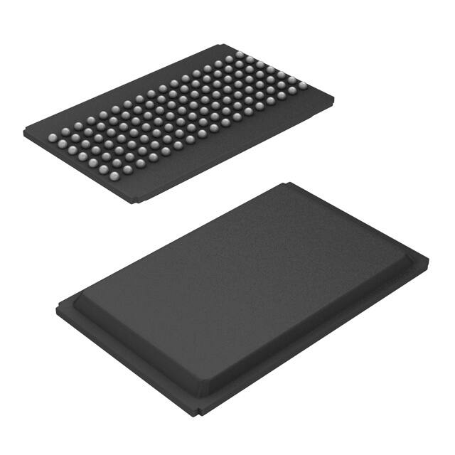
Available in non Pb-free 119 ball PBGA.
Writing the data bytes into the SRAM is accomplished when the
chip select controlling that byte is LOW and the write enable input
(WE) input is LOW. Data on the respective input/output (I/O) pins
is then written into the location specified on the address pins
(A0–A18). Asserting all of the chip selects LOW and write enable
LOW will write all 24 bits of data into the SRAM. Output enable
(OE) is ignored while in WRITE mode.
Data bytes can also be individually read from the device.
Reading a byte is accomplished when the chip select controlling
that byte is LOW and write enable (WE) HIGH while output
enable (OE) remains LOW. Under these conditions, the contents
of the memory location specified on the address pins will appear
on the specified data input/output (I/O) pins. Asserting all the chip
selects LOW will read all 24 bits of data from the SRAM.
The 24 I/O pins (I/O0–I/O23) are placed in a high-impedance
state when all the chip selects are HIGH or when the output
enable (OE) is HIGH during a READ mode. For further details,
refer to the truth table of this data sheet.
The CY7C1012AV33 is available in a standard 119-ball PBGA.
For a complete list of related documentation, click here.
Functional Block Diagram
512K x 24
ARRAY
I/O8–I/O15
I/O16–I/O23
CONTROL LOGIC
CE0, CE1, CE2
WE
OE
A10
A11
A 12
A 13
A 14
A15
A16
A17
A18
COLUMN
DECODER
I/O0–I/O7
SENSE AMPS
A0
A1
A2
A3
A4
A5
A6
A7
A8
A9
ROW DECODER
INPUT BUFFER
Cypress Semiconductor Corporation
Document Number: 38-05254 Rev. *J
•
198 Champion Court
•
San Jose, CA 95134-1709
•
408-943-2600
Revised November 18, 2014
�CY7C1012AV33
Contents
Selection Guide ................................................................ 3
Pin Configurations ........................................................... 3
Maximum Ratings ............................................................. 4
Operating Range ............................................................... 4
DC Electrical Characteristics .......................................... 4
Capacitance ...................................................................... 5
AC Test Loads and Waveforms ....................................... 5
AC Switching Characteristics ......................................... 6
Switching Waveforms ...................................................... 7
Truth Table ........................................................................ 9
Ordering Information ...................................................... 10
Ordering Code Definitions ......................................... 10
Document Number: 38-05254 Rev. *J
Package Diagram ............................................................ 11
Acronyms ........................................................................ 12
Document Conventions ................................................. 12
Units of Measure ....................................................... 12
Document History Page ................................................. 13
Sales, Solutions, and Legal Information ...................... 14
Worldwide Sales and Design Support ....................... 14
Products .................................................................... 14
PSoC® Solutions ...................................................... 14
Cypress Developer Community ................................. 14
Technical Support ..................................................... 14
Page 2 of 14
�CY7C1012AV33
Selection Guide
Description
Maximum Access Time
Maximum Operating Current
Commercial
Industrial
Commercial / Industrial
Maximum CMOS Standby Current
-8
8
300
300
50
Unit
ns
mA
mA
Pin Configurations
Figure 1. 119-ball PBGA pinout (Top View) [1, 2]
1
2
3
4
5
6
7
A
NC
A
A
A
A
A
NC
B
NC
A
A
CE0
A
A
NC
C
I/O12
NC
CE1
NC
CE2
NC
I/O0
D
I/O13
VDD
VSS
VSS
VSS
VDD
I/O1
E
I/O14
VSS
VDD
VSS
VDD
VSS
I/O2
F
I/O15
VDD
VSS
VSS
VSS
VDD
I/O3
G
I/O16
VSS
VDD
VSS
VDD
VSS
I/O4
H
I/O17
VDD
VSS
VSS
VSS
VDD
I/O5
J
NC
VSS
VDD
VSS
VDD
VSS
DNU
K
I/O18
VDD
VSS
VSS
VSS
VDD
I/O6
L
I/O19
VSS
VDD
VSS
VDD
VSS
I/O7
M
I/O20
VDD
VSS
VSS
VSS
VDD
I/O8
N
I/O21
VSS
VDD
VSS
VDD
VSS
I/O9
P
I/O22
VDD
VSS
VSS
VSS
VDD
I/O10
R
I/O23
A
NC
NC
NC
A
I/O11
T
NC
A
A
WE
A
A
NC
U
NC
A
A
OE
A
A
NC
Notes
1. NC pins are not connected on the die.
2. DNU pins have to be left floating or tied to VSS to ensure proper application.
Document Number: 38-05254 Rev. *J
Page 3 of 14
�CY7C1012AV33
Maximum Ratings
DC Voltage Applied to Outputs
in high Z State [3] ................................ –0.5 V to VCC + 0.5 V
Exceeding maximum ratings may shorten the useful life of the
device. User guidelines are not tested.
DC Input Voltage [3] ............................ –0.5 V to VCC + 0.5 V
Current into Outputs (LOW) ........................................ 20 mA
Storage Temperature ............................... –65 C to +150 C
Operating Range
Ambient Temperature with
Power Applied ......................................... –55 C to +125 C
Range
Supply Voltage on
VCC to Relative GND[3] ................................–0.5 V to +4.6 V
Ambient Temperature
VCC
0 C to +70 C
3.3 V 0.3 V
Commercial
–40 C to +85 C
Industrial
DC Electrical Characteristics
Over the Operating Range
Parameter
Description
Test Conditions [4]
-8
Unit
Min
Max
2.4
–
V
–
0.4
V
VOH
Output HIGH Voltage
VCC = Min, IOH = –4.0 mA
VOL
Output LOW Voltage
VCC = Min, IOL = 8.0 mA
VIH
Input HIGH Voltage
2.0
VCC + 0.3
V
VIL[3]
Input LOW Voltage
–0.3
0.8
V
IIX
Input Leakage Current
GND < VI < VCC
–1
+1
A
IOZ
Output Leakage Current
GND < VOUT < VCC, Output Disabled
–1
+1
A
ICC
VCC Operating Supply Current
VCC = Max,
f = fMAX = 1/tRC
Commercial
–
300
mA
Industrial
–
300
mA
–
100
mA
–
50
mA
ISB1
Automatic CE Power-down
Current – TTL Inputs
Max VCC, CE > VIH,
VIN > VIH or VIN < VIL, f = fMAX
ISB2
Automatic CE Power-down
Current – CMOS Inputs
Max VCC,
CE > VCC – 0.3 V,
VIN > VCC – 0.3 V,
or VIN < 0.3 V, f = 0
Commercial /
Industrial
Notes
3. VIL (min) = –2.0 V for pulse durations of less than 20 ns.
4. CE refers to a combination of CE0, CE1, and CE2. CE is active LOW when all three of these signals are active LOW at the same time.
Document Number: 38-05254 Rev. *J
Page 4 of 14
�CY7C1012AV33
Capacitance
Parameter [5]
Description
CIN
Input Capacitance
COUT
I/O Capacitance
Test Conditions
TA = 25 C, f = 1 MHz, VCC = 3.3 V
Max
Unit
8
pF
10
pF
AC Test Loads and Waveforms
Figure 2. AC Test Loads and Waveforms [6]
50
VTH = 1.5 V
OUTPUT
Z0 = 50
(a)
OUTPUT
30 pF* * Capacitive Load consists of all
components of the test environment.
3.3 V
GND
Rise time > 1 V/ns
R1 317
3.3 V
INCLUDING
JIG AND
SCOPE
ALL INPUT PULSES
90%
R2
351
5 pF
(b)
90%
10%
10%
(c)
Fall time: > 1 V/ns
Notes
5. Tested initially and after any design or process changes that may affect these parameters.
6. Valid SRAM operation does not occur until the power supplies have reached the minimum operating VDD (3.0 V). As soon as 1 ms (Tpower) after reaching the minimum
operating VDD, normal SRAM operation can begin including reduction in VDD to the data retention (VCCDR, 2.0 V) voltage.
Document Number: 38-05254 Rev. *J
Page 5 of 14
�CY7C1012AV33
AC Switching Characteristics
Over the Operating Range
Parameter [7]
Description
-8
Min
Max
Unit
Read Cycle
tpower[8]
VCC(typical) to the first access
1
–
ms
tRC
Read Cycle Time
8
–
ns
tAA
Address to Data Valid
–
8
ns
tOHA
Data Hold from Address Change
3
–
ns
tACE
CE1, CE2, and CE3 LOW to Data Valid
–
8
ns
tDOE
OE LOW to Data Valid
–
5
ns
1
–
ns
tLZOE
tHZOE
OE LOW to low
Z[9]
–
5
ns
tLZCE
CE1, CE2, and CE3 LOW to low
Z[9]
3
–
ns
tHZCE
CE1, CE2, or CE3 HIGH to high Z[9]
–
5
ns
power-up[10]
0
–
ns
power-down[10]
–
8
ns
tPU
OE HIGH to high
Z[9]
CE1, CE2, and CE3 LOW to
tPD
CE1, CE2, or CE3 HIGH to
tDBE
Byte Enable to Data Valid
–
5
ns
tLZBE
Byte Enable to low Z[9]
1
–
ns
–
5
ns
tHZBE
Write
Byte Disable to high
Z[9]
Cycle[11, 12]
tWC
Write Cycle Time
8
–
ns
tSCE
CE1, CE2, and CE3 LOW to Write End
6
–
ns
tAW
Address Set-up to Write End
6
–
ns
tHA
Address Hold from Write End
0
–
ns
tSA
Address Set-up to Write Start
0
–
ns
tPWE
WE Pulse Width
6
–
ns
tSD
Data Set-up to Write End
5
–
ns
tHD
Data Hold from Write End
0
–
ns
tLZWE
WE HIGH to low
Z[13]
3
–
ns
tHZWE
WE LOW to high Z[13]
–
5
ns
tBW
Byte Enable to End of Write
6
–
ns
Notes
7. Test conditions assume signal transition time of 3 ns or less, timing reference levels of 1.5 V, input pulse levels of 0 to 3.0 V, and output loading of the specified IOL/IOH
and transmission line loads. Test conditions for the read cycle use output loading as shown in part (a) of the Figure 2, unless specified otherwise.
8. This part has a voltage regulator which steps down the voltage from 3 V to 2 V internally. tpower time has to be provided initially before a read/write operation is started.
9. tHZOE, tHZCE, tHZWE, tHZBE, and tLZOE, tLZCE, tLZWE, tLZBE are specified with a load capacitance of 5 pF as in part (b) of Figure 2. Transition is measured 200 mV
from steady-state voltage.
10. These parameters are guaranteed by design and are not tested.
11. The internal write time of the memory is defined by the overlap of CE1, CE2, and CE3 LOW and WE LOW. The chip enables must be active and WE must be LOW
to initiate a write, and the transition of any of these signals can terminate the write. The input data set-up and hold timing should be referenced to the leading edge
of the signal that terminates the write.
12. The minimum write cycle time for Write Cycle No. 3 (WE controlled, OE LOW) is the sum of tHZWE and tSD.
13. tHZOE, tHZCE, tHZWE, tHZBE, and tLZOE, tLZCE, tLZWE, tLZBE are specified with a load capacitance of 5 pF as in part (b) of Figure 2 on page 5. Transition is measured
200 mV from steady-state voltage.
Document Number: 38-05254 Rev. *J
Page 6 of 14
�CY7C1012AV33
Switching Waveforms
Figure 3. Read Cycle No. 1 [14, 15]
tRC
ADDRESS
tOHA
DATA OUT
tAA
PREVIOUS DATA VALID
DATA VALID
Figure 4. Read Cycle No. 2 (OE Controlled) [15, 16, 17]
ADDRESS
tRC
CE
tACE
OE
tHZOE
tDOE
DATA OUT
tHZCE
tLZOE
HIGH IMPEDANCE
DATA VALID
tLZCE
VCC
SUPPLY
CURRENT
HIGH
IMPEDANCE
tPD
tPU
50%
50%
ICC
ISB
Figure 5. Write Cycle No. 1 (CE Controlled) [17, 18, 19]
tWC
ADDRESS
tSCE
CE
tSA
tSCE
tAW
tHA
tPWE
WE
tSD
DATA I/O
tHD
DATA VALID
Notes
14. Device is continuously selected. OE, CE = VIL.
15. WE is HIGH for read cycle.
16. Address valid prior to or coincident with CE transition LOW.
17. CE refers to a combination of CE0, CE1, and CE2. CE is active LOW when all three of these signals are active LOW at the same time.
18. Data I/O is high impedance if OE = VIH.
19. If CE goes HIGH simultaneously with WE going HIGH, the output remains in a high-impedance state.
Document Number: 38-05254 Rev. *J
Page 7 of 14
�CY7C1012AV33
Switching Waveforms (continued)
Figure 6. Write Cycle No. 2 (WE Controlled, OE HIGH During Write) [20, 21]
tWC
ADDRESS
tSCE
CE
tAW
tHA
tSA
tPWE
WE
OE
tSD
DATA I/O
tHD
DATAIN VALID
NOTE 22
tHZOE
Figure 7. Write Cycle No. 3 (WE Controlled, OE LOW) [21, 23]
tWC
ADDRESS
tSCE
CE
tAW
tSA
tHA
tPWE
WE
tSD
DATA I/O
NOTE 22
tHD
DATA VALID
tHZWE
tLZWE
Notes
20. Data I/O is high impedance if OE = VIH.
21. If CE goes HIGH simultaneously with WE going HIGH, the output remains in a high-impedance state.
22. During this period the I/Os are in the output state and input signals should not be applied.
23. CE refers to a combination of CE0, CE1, and CE2. CE is active LOW when all three of these signals are active LOW at the same time.
Document Number: 38-05254 Rev. *J
Page 8 of 14
�CY7C1012AV33
Truth Table
CE0
CE1
CE2
OE
WE
I/O0–I/O23
Mode
Power
H
H
H
X
X
High Z
Power-down
Standby (ISB)
L
H
H
L
H
I/O0–I/O7 Data Out
Read
Active (ICC)
H
L
H
L
H
I/O8–I/O15 Data Out
Read
Active (ICC)
H
H
L
L
H
I/O16–I/O23 Data Out
Read
Active (ICC)
L
L
L
L
H
Full Data Out
Read
Active (ICC)
L
H
H
X
L
I/O0–I/O7 Data In
Write
Active (ICC)
H
L
H
X
L
I/O8–I/O15 Data In
Write
Active (ICC)
H
H
L
X
L
I/O16–I/O23 Data In
Write
Active (ICC)
L
L
L
X
L
Full Data In
Write
Active (ICC)
L
L
L
H
H
High Z
Selected, Outputs Disabled
Active (ICC)
Document Number: 38-05254 Rev. *J
Page 9 of 14
�CY7C1012AV33
Ordering Information
Speed
(ns)
8
Package
Diagram
Ordering Code
CY7C1012AV33-8BGC
Package Type
51-85115 119-ball (14 × 22 × 2.4 mm) PBGA
Operating
Range
Commercial
Ordering Code Definitions
CY 7
C 1012 A
V33 - 8
BG
C
Temperature range: C = Commercial
BG = 119-ball PBGA
Speed Grade: 8 ns
V33 = 3.3 V
Process Technology: A 90 nm
Part Identifier
Technology Code: C = CMOS
Marketing Code: 7 = SRAM
Company ID: CY = Cypress
Document Number: 38-05254 Rev. *J
Page 10 of 14
�CY7C1012AV33
Package Diagram
Figure 8. 119-ball PBGA (14 × 22 × 2.4 mm) BG119 Package Outline, 51-85115
51-85115 *D
Document Number: 38-05254 Rev. *J
Page 11 of 14
�CY7C1012AV33
Acronyms
Acronym
Document Conventions
Description
Units of Measure
CMOS
Complementary Metal Oxide Semiconductor
CE
Chip Enable
°C
degree Celsius
I/O
Input/Output
MHz
megahertz
OE
Output Enable
µA
microampere
PBGA
Plastic Ball Grid Array
mA
milliampere
SRAM
Static Random Access Memory
mm
millimeter
TTL
Transistor-Transistor Logic
ms
millisecond
WE
Write Enable
mV
millivolt
mW
milliwatt
Document Number: 38-05254 Rev. *J
Symbol
Unit of Measure
ns
nanosecond
%
percent
pF
picofarad
V
volt
W
watt
Page 12 of 14
�CY7C1012AV33
Document History Page
Document Title: CY7C1012AV33, 512 K × 24 Static RAM
Document Number: 38-05254
Rev.
ECN No.
Issue Date
Orig. of
Change
**
113711
03/11/02
NSL
Description of Change
New data sheet.
*A
117057
07/31/02
DFP
Removed 15-ns bin
*B
117988
09/03/02
DFP
Added 8-ns bin
*C
118992
09/19/02
DFP
Change Cin (input capacitance) from 6 pF to 8 pF
Change Cout (output capacitance) from 8 pF to 10 pF
*D
120382
11/15/02
DFP
Final data sheet. Added note 4 to “AC Test Loads and Waveforms”
*E
492137
See ECN
NXR
Removed 12 ns speed bin from product offering
Included note #1 and 2 on page #2
Changed the description of IIX from Input Load Current to Input Leakage Current in DC Electrical Characteristics table
Updated Ordering Information Table
*F
2896044
03/19/2010
AJU
Updated Ordering Information Table
Updated Package Diagram
Added Sales, Solutions, and Legal Information
*G
3097955
11/30/2010
PRAS
*H
3086499
06/07/2011
AJU
Updated Selection Guide (Removed -10 column).
Updated DC Electrical Characteristics (Removed -10 column).
Updated AC Switching Characteristics (Removed -10 column).
Updated in new template.
*I
4212876
12/06/2013
VINI
Updated Package Diagram:
spec 51-85115 – Changed revision from *C to *D.
Updated in new template.
Completing Sunset Review.
*J
4573215
11/18/2014
VINI
Added related documentation hyperlink in page 1.
Document Number: 38-05254 Rev. *J
Added Ordering Code Definitions.
Added Acronyms and Units of Measure.
Minor edits.
Page 13 of 14
�CY7C1012AV33
Sales, Solutions, and Legal Information
Worldwide Sales and Design Support
Cypress maintains a worldwide network of offices, solution centers, manufacturer’s representatives, and distributors. To find the office
closest to you, visit us at Cypress Locations.
PSoC® Solutions
Products
Automotive
cypress.com/go/automotive
Clocks & Buffers
Interface
Lighting & Power Control
cypress.com/go/clocks
cypress.com/go/interface
cypress.com/go/powerpsoc
cypress.com/go/plc
Memory
cypress.com/go/memory
PSoC
cypress.com/go/psoc
Touch Sensing
PSoC 1 | PSoC 3 | PSoC 4 | PSoC 5LP
Cypress Developer Community
Community | Forums | Blogs | Video | Training
Technical Support
cypress.com/go/support
cypress.com/go/touch
USB Controllers
Wireless/RF
psoc.cypress.com/solutions
cypress.com/go/USB
cypress.com/go/wireless
© Cypress Semiconductor Corporation, 2002-2014. The information contained herein is subject to change without notice. Cypress Semiconductor Corporation assumes no responsibility for the use of
any circuitry other than circuitry embodied in a Cypress product. Nor does it convey or imply any license under patent or other rights. Cypress products are not warranted nor intended to be used for
medical, life support, life saving, critical control or safety applications, unless pursuant to an express written agreement with Cypress. Furthermore, Cypress does not authorize its products for use as
critical components in life-support systems where a malfunction or failure may reasonably be expected to result in significant injury to the user. The inclusion of Cypress products in life-support systems
application implies that the manufacturer assumes all risk of such use and in doing so indemnifies Cypress against all charges.
Any Source Code (software and/or firmware) is owned by Cypress Semiconductor Corporation (Cypress) and is protected by and subject to worldwide patent protection (United States and foreign),
United States copyright laws and international treaty provisions. Cypress hereby grants to licensee a personal, non-exclusive, non-transferable license to copy, use, modify, create derivative works of,
and compile the Cypress Source Code and derivative works for the sole purpose of creating custom software and or firmware in support of licensee product to be used only in conjunction with a Cypress
integrated circuit as specified in the applicable agreement. Any reproduction, modification, translation, compilation, or representation of this Source Code except as specified above is prohibited without
the express written permission of Cypress.
Disclaimer: CYPRESS MAKES NO WARRANTY OF ANY KIND, EXPRESS OR IMPLIED, WITH REGARD TO THIS MATERIAL, INCLUDING, BUT NOT LIMITED TO, THE IMPLIED WARRANTIES
OF MERCHANTABILITY AND FITNESS FOR A PARTICULAR PURPOSE. Cypress reserves the right to make changes without further notice to the materials described herein. Cypress does not
assume any liability arising out of the application or use of any product or circuit described herein. Cypress does not authorize its products for use as critical components in life-support systems where
a malfunction or failure may reasonably be expected to result in significant injury to the user. The inclusion of Cypress’ product in a life-support systems application implies that the manufacturer
assumes all risk of such use and in doing so indemnifies Cypress against all charges.
Use may be limited by and subject to the applicable Cypress software license agreement.
Document Number: 38-05254 Rev. *J
Revised November 18, 2014
All products and company names mentioned in this document may be the trademarks of their respective holders.
Page 14 of 14
�