CY7C1019BN
128K x 8 Static RAM
Features
• High speed — tAA = 12, 15 ns • CMOS for optimum speed/power • Center power/ground pinout • Automatic power-down when deselected • Easy memory expansion with CE and OE options • Functionally equivalent to CY7C1019
Functional Description
The CY7C1019BN is a high-performance CMOS static RAM organized as 131,072 words by 8 bits. Easy memory expansion is provided by an active LOW Chip Enable (CE), an active LOW Output Enable (OE), and three-state drivers. This device has an automatic power-down feature that significantly reduces power consumption when deselected. Writing to the device is accomplished by taking Chip Enable (CE) and Write Enable (WE) inputs LOW. Data on the eight I/O pins (I/O0 through I/O7) is then written into the location specified on the address pins (A0 through A16). Reading from the device is accomplished by taking Chip Enable (CE) and Output Enable (OE) LOW while forcing Write Enable (WE) HIGH. Under these conditions, the contents of the memory location specified by the address pins will appear on the I/O pins. The eight input/output pins (I/O0 through I/O7) are placed in a high-impedance state when the device is deselected (CE HIGH), the outputs are disabled (OE HIGH), or during a write operation (CE LOW, and WE LOW). The CY7C1019BN is available in standard 32-pin TSOP Type II and 400-mil-wide SOJ packages.
Logic Block Diagram
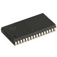
Pin Configurations
SOJ / TSOPII Top View
A0 A1 A2 A3 CE I/O0 I/O1 VCC V SS I/O2 I/O3 WE A4 A5 A6 A7 1 2 3 4 5 6 7 8 9 10 11 12 13 14 15 16 32 31 30 29 28 27 26 25 24 23 22 21 20 19 18 17 A16 A15 A14 A13 OE I/O7 I/O6 VSS VCC I/O5 I/O4 A12 A11 A10 A9 A8
I/O0
INPUT BUFFER
A0 A1 A2 A3 A4 A5 A6 A7 A8
I/O1
ROW DECODER
I/O2
SENSE AMPS 512 x 256 x 8 ARRAY
I/O3 I/O4 I/O5
CE WE OE
COLUMN DECODER
POWER DOWN
I/O6 I/O7
A9 A 10 A 11 A 12 A 13 A 14 A 15 A 16
Cypress Semiconductor Corporation Document #: 001-06425 Rev. **
•
198 Champion Court
•
San Jose, CA 95134-1709 • 408-943-2600 Revised February 1, 2006
�CY7C1019BN
Selection Guide
7C1019BN-12 Maximum Access Time Maximum Operating Current Maximum Standby Current L 12 140 10 1 7C1019BN-15 15 130 10 1 Unit ns mA mA mA
Maximum Ratings
(Above which the useful life may be impaired. For user guidelines, not tested.) Storage Temperature ................................. –65°C to +150°C Ambient Temperature with Power Applied............................................. –55°C to +125°C Supply Voltage on VCC to Relative GND[1] .... –0.5V to +7.0V DC Voltage Applied to Outputs in High Z State[1] ....................................–0.5V to VCC + 0.5V DC Input Voltage[1] .................................–0.5V to VCC + 0.5V
Current into Outputs (LOW)......................................... 20 mA Static Discharge Voltage............................................ >2001V (per MIL-STD-883, Method 3015) Latch-Up Current ..................................................... >200 mA
Operating Range
Range Commercial Industrial Ambient Temperature[2] 0°C to +70°C –40°C to +85°C VCC 5V ± 10% 5V ± 10%
Electrical Characteristics Over the Operating Range
-12 Parameter VOH VOL VIH VIL IIX IOZ ICC ISB1 Description Test Conditions Min. 2.4 0.4 2.2 –0.3 GND < VI < VCC GND < VI < VCC, Output Disabled VCC = Max., IOUT = 0 mA, f = fMAX = 1/tRC L –1 –5 VCC+ 0.3 0.8 +1 +5 140 40 20 10 L 1 2.2 –0.3 –1 –5 Max. Min. 2.4 0.4 VCC+ 0.3 0.8 +1 +5 130 40 20 10 1 mA Output HIGH Voltage VCC = Min., IOH = – 4.0 mA Output LOW Voltage VCC = Min., IOL = 8.0 mA Input HIGH Voltage Input LOW Voltage[1] Input Leakage Current Output Leakage Current VCC Operating Supply Current -15 Max. Unit V V V V µA µA mA mA
ISB2
Automatic CE Max. VCC, CE > VIH Power-Down Current VIN > VIH or VIN < VIL, f = fMAX —TTL Inputs Automatic CE Max. VCC, Power-Down Current CE > VCC – 0.3V, —CMOS Inputs VIN > VCC – 0.3V, or VIN < 0.3V, f = 0
Capacitance[3]
Parameter CIN COUT Description Input Capacitance Output Capacitance Test Conditions TA = 25°C, f = 1 MHz, VCC = 5.0V Max. 6 8 Unit pF pF
Notes: 1. VIL (min.) = –2.0V for pulse durations of less than 20 ns. 2. TA is the “Instant On” case temperature. 3. Tested initially and after any design or process changes that may affect these parameters.
Document #: 001-06425 Rev. **
Page 2 of 8
�CY7C1019BN
AC Test Loads and Waveforms
R1 480Ω R1 480Ω 5V OUTPUT 30 pF INCLUDING JIG AND SCOPE (a) R2 255 Ω 5 pF INCLUDING JIG AND SCOPE (b) R2 255Ω GND ≤ 3 ns 3.0V 90% 10% 90% 10% ≤ 3 ns ALL INPUT PULSES
5V OUTPUT
Equivalent to: THÉVENIN EQUIVALENT 167 Ω 1.73V OUTPUT
Switching Characteristics[4] Over the Operating Range
-12 Parameter Read Cycle tRC tAA tOHA tACE tDOE tLZOE tHZOE tLZCE tHZCE tPU tPD Write Cycle[7, 8] tWC tSCE tAW tHA tSA tPWE tSD tHD tLZWE tHZWE Write Cycle Time CE LOW to Write End Address Set-Up to Write End Address Hold from Write End Address Set-Up to Write Start WE Pulse Width Data Set-Up to Write End Data Hold from Write End WE HIGH to Low Z[6] WE LOW to High Z[5, 6] 12 9 8 0 0 8 6 0 3 6 15 10 10 0 0 10 8 0 3 7 ns ns ns ns ns ns ns ns ns ns Read Cycle Time Address to Data Valid Data Hold from Address Change CE LOW to Data Valid OE LOW to Data Valid OE LOW to Low Z OE HIGH to High CE HIGH to High Z[5, 6] 3 6 0 12 0 15 Z[5, 6] CE LOW to Low Z[6] CE LOW to Power-Up CE HIGH to Power-Down 0 6 3 7 3 12 6 0 7 12 12 3 15 7 15 15 ns ns ns ns ns ns ns ns ns ns ns Description Min. Max. Min. -15 Max. Unit
Notes: 4. Test conditions assume signal transition time of 3 ns or less, timing reference levels of 1.5V, input pulse levels of 0 to 3.0V, and output loading of the specified IOL/IOH and 30-pF load capacitance. 5. tHZOE, tHZCE, and tHZWE are specified with a load capacitance of 5 pF as in part (b) of AC Test Loads. Transition is measured ±500 mV from steady-state voltage. 6. At any given temperature and voltage condition, tHZCE is less than tLZCE, tHZOE is less than tLZOE, and tHZWE is less than tLZWE for any given device. 7. The internal write time of the memory is defined by the overlap of CE LOW and WE LOW. CE and WE must be LOW to initiate a write, and the transition of any of these signals can terminate the write. The input data set-up and hold timing should be referenced to the leading edge of the signal that terminates the write. 8. The minimum write cycle time for Write Cycle no. 3 (WE controlled, OE LOW) is the sum of tHZWE and tSD.
Document #: 001-06425 Rev. **
Page 3 of 8
�CY7C1019BN
Data Retention Characteristics Over the Operating Range (L Version Only)
Parameter VDR ICCDR tCDR[3] tR Description VCC for Data Retention Data Retention Current Chip Deselect to Data Retention Time Operation Recovery Time Conditions No input may exceed VCC + 0.5V VCC = VDR = 2.0V, CE > VCC – 0.3V, VIN > VCC – 0.3V or VIN < 0.3V Min. 2.0 300 0 200 Max. Unit V µA ns µs
Data Retention Waveform
DATA RETENTION MODE VCC 3.0V tCDR CE VDR > 2V 3.0V tR
Switching Waveforms
Read Cycle No. 1[9, 10]
tRC ADDRESS tAA tOHA DATA OUT PREVIOUS DATA VALID DATA VALID
Read Cycle No. 2 (OE Controlled)[10, 11]
ADDRESS tRC CE tACE OE tDOE DATA OUT VCC SUPPLY CURRENT tLZOE HIGH IMPEDANCE tLZCE tPU 50% tHZOE tHZCE DATA VALID tPD 50% ISB ICC HIGH IMPEDANCE
Notes: 9. Device is continuously selected. OE, CE = VIL. 10. WE is HIGH for read cycle. 11. Address valid prior to or coincident with CE transition LOW.
Document #: 001-06425 Rev. **
Page 4 of 8
�CY7C1019BN
Switching Waveforms (continued)
Write Cycle No. 1 (CE Controlled)[12, 13]
tWC ADDRESS tSCE CE tSA tSCE tAW tPWE WE tSD DATA I/O DATA VALID tHD tHA
Write Cycle No. 2 (WE Controlled, OE HIGH During Write)[12, 13]
tWC ADDRESS tSCE CE
tAW tSA WE tPWE
tHA
OE tSD DATA I/O NOTE 14 tHZOE
Notes: 12. Data I/O is high impedance if OE = VIH. 13. If CE goes HIGH simultaneously with WE going HIGH, the output remains in a high-impedance state. 14. During this period the I/Os are in the output state and input signals should not be applied.
tHD
DATAIN VALID
Document #: 001-06425 Rev. **
Page 5 of 8
�CY7C1019BN
Switching Waveforms (continued)
Write Cycle No. 3 (WE Controlled, OE LOW)[13]
tWC ADDRESS tSCE CE tAW tSA WE tSD DATA I/O NOTE 14 tHZWE DATA VALID tLZWE tHD tPWE tHA
Truth Table
CE H L L L OE X L X H WE X H L H High Z Data Out Data In High Z I/O0–I/O7 Power-Down Read Write Selected, Outputs Disabled Mode Power Standby (ISB) Active (ICC) Active (ICC) Active (ICC)
Ordering Information
Speed (ns) 12 Ordering Code CY7C1019BN-12VC CY7C1019BN-12ZC CY7C1019BN-12ZXC CY7C1019BN-15VC CY7C1019BN-15ZXC Package Diagram Package Type 51-85033 32-Lead 400-Mil Molded SOJ 51-85095 32-Lead TSOP Type II 51-85095 32-Lead TSOP Type II (Pb-free) 51-85033 32-Lead 400-Mil Molded SOJ 51-85095 32-Lead TSOP Type II (Pb-free) Operating Range Commercial
15
Commercial
Please contact local sales representative regarding availability of these parts
Document #: 001-06425 Rev. **
Page 6 of 8
�CY7C1019BN
Package Diagrams
32-pin (400-mil) Molded SOJ (51-85033)
51-85033-A
51-85033-*B
32-pin TSOP II (51-85095)
51-85095-**
All product or company names mentioned in this document may be the trademarks of their respective holders. Document #: 001-06425 Rev. ** Page 7 of 8
© Cypress Semiconductor Corporation, 2006. The information contained herein is subject to change without notice. Cypress Semiconductor Corporation assumes no responsibility for the use of any circuitry other than circuitry embodied in a Cypress product. Nor does it convey or imply any license under patent or other rights. Cypress products are not warranted nor intended to be used for medical, life support, life saving, critical control or safety applications, unless pursuant to an express written agreement with Cypress. Furthermore, Cypress does not authorize its products for use as critical components in life-support systems where a malfunction or failure may reasonably be expected to result in significant injury to the user. The inclusion of Cypress products in life-support systems application implies that the manufacturer assumes all risk of such use and in doing so indemnifies Cypress against all charges.
�CY7C1019BN
Document History Page
Document Title: CY7C1019BN 128K x 8 Static RAM Document Number: 001-06425 REV. ** ECN NO. 423847 Issue Date See ECN Orig. of Change NXR New Data Sheet Description of Change
Document #: 001-06425 Rev. **
Page 8 of 8
�