032
CY7C1031
CY7C1032
64K x 18 Synchronous
Cache RAM
Features
Functional Description
• Supports 66-MHz Pentium® microprocessor cache systems with zero wait states
• 64K by 18 common I/O
• Fast clock-to-output times
— 8.5 ns
• Two-bit wraparound counter supporting Pentium microprocessor and 486 burst sequence (7C1031)
• Two-bit wraparound counter supporting linear burst sequence (7C1032)
• Separate processor and controller address strobes
• Synchronous self-timed write
• Direct interface with the processor and external cache
controller
• Asynchronous output enable
• I/Os capable of 3.3V operation
• JEDEC-standard pinout
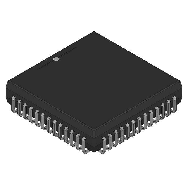
• 52-pin PLCC packaging
The CY7C1031 and CY7C1032 are 64K by 18 synchronous
cache RAMs designed to interface with high-speed microprocessors with minimum glue logic. Maximum access delay from
clock rise is 8.5 ns. A 2-bit on-chip counter captures the first
address in a burst and increments the address automatically
for the rest of the burst access.
The CY7C1031 is designed for Intel® Pentium and i486 CPUbased systems; its counter follows the burst sequence of the
Pentium and the i486 processors. The CY7C1032 is architected for processors with linear burst sequences. Burst accesses
can be initiated with the processor address strobe (ADSP) or
the cache controller address strobe (ADSC) inputs. Address
advancement is controlled by the address advancement (ADV)
input.
A synchronous self-timed write mechanism is provided to simplify the write interface. A synchronous chip select input and
an asynchronous output enable input provide easy control for
bank selection and output three-state control.
Logic Block Diagram
Pin Configuration
A15 –A0
ADDR
REG
9
9
DQ8
DQ9
VCCQ
VSSQ
DQ10
DQ11
DQ12
DQ13
VSSQ
VCCQ
DQ14
DQ15
DP1[1]
14
16
2
2
ADV
LOGIC
WH
CLK
ADSP
ADSC
CS
WH
WL
64K X 9
64K X 9
RAM ARRAY RAM ARRAY
TIMING
CONTROL
WL
9
9
OE
A8
A9
A10
7 6 5 4 3 2 1 52 51 50 49 48 47
46
45
44
43
42
41
7C1031
7C1032
40
39
38
37
36
35
34
2122 23 24 25 26 27 28 29 30 31 32 33
[1]
DP0
DQ7
DQ6
VCCQ
VSSQ
DQ5
DQ4
DQ3
DQ2
VSSQ
VCCQ
DQ1
DQ0
A5
A
4
A
3
A
2
A1
A0
GND
V CC
A
15
A14
A13
A12
A11
ADV
8
9
10
11
12
13
14
15
16
17
18
19
20
WH
WL
ADSC
ADSP
DATA IN
REGISTER
14
A6
A7
CS
16
ADV
CLK
PLCC
Top View
18
18
DQ15 – DQ0
DP1 – DP0
OE
Selection Guide
Maximum Access Time (ns)
Maximum Operating Current (mA)
Commercial
7C1031-8
7C1032-8
7C1031-10
7C1032-10
7C1031-12
7C1032-12
8.5
10
12
280
280
230
Intel and Pentium are trademarks of Intel Corporation.
Note:
1. DP0 and DP1 are functionally equivalent to DQx.
Cypress Semiconductor Corporation
Document #: 38-05278 Rev. **
•
3901 North First Street
•
San Jose
•
CA 95134 • 408-943-2600
Revised March 15, 2002
�CY7C1031
CY7C1032
Functional Description (continued)
Single Write Accesses Initiated by ADSP
This access is initiated when the following conditions are satisfied at clock rise: (1) CS is LOW and (2) ADSP is LOW.
ADSP-triggered write cycles are completed in two clock periods. The address at A0 through A15 is loaded into the address
register and address advancement logic and delivered to the
RAM core. The write signal is ignored in this cycle because the
cache tag or other external logic uses this clock period to perform address comparisons or protection checks. If the write is
allowed to proceed, the write input to the CY7C1031 and
CY7C1032 will be pulled LOW before the next clock rise.
ADSP is ignored if CS is HIGH.
If WH, WL, or both are LOW at the next clock rise, information
presented at DQ0–DQ15 and DP0–DP1 will be written into the
location specified by the address advancement logic. WL controls the writing of DQ0–DQ7 and DP0 while WH controls the
writing of DQ8–DQ15 and DP1. Because the CY7C1031 and
CY7C1032 are common-I/O devices, the output enable signal
(OE) must be deasserted before data from the CPU is delivered to DQ0–DQ15 and DP0–DP1. As a safety precaution, the
appropriate data lines are three-stated in the cycle where WH,
WL, or both are sampled LOW, regardless of the state of the
OE input.
Single Write Accesses Initiated by ADSC
This write access is initiated when the following conditions are
satisfied at rising edge of the clock: (1) CS is LOW, (2) ADSC
is LOW, and (3) WH or WL are LOW. ADSC-triggered accesses are completed in a single clock cycle.
The address at A0 through A15 is loaded into the address register and address advancement logic and delivered to the RAM
core. Information presented at DQ0–DQ15 and DP0–DP1 will
be written into the location specified by the address advancement logic. Since the CY7C1031 and the CY7C1032 are common-I/O devices, the output enable signal (OE) must be deasserted before data from the cache controller is delivered to the
data and parity lines. As a safety precaution, the appropriate
data and parity lines are three-stated in the cycle where WH
and WL are sampled LOW regardless of the state of the OE
input.
Single Read Accesses
is LOW, and (3) WH and WL are HIGH. The address at A0
through A15 is stored into the address advancement logic and
delivered to the RAM core. If the output enable (OE) signal is
asserted (LOW), data will be available at the data outputs a
maximum of 8.5 ns after clock rise. ADSP is ignored if CS is
HIGH.
Burst Sequences
The CY7C1031 provides a 2-bit wraparound counter, fed by
pins A0–A1, that implements the Intel 80486 and Pentium processor’s address burst sequence (see Table 1). Note that the
burst sequence depends on the first burst address.
Table 1. Counter Implementation for the Intel
Pentium/80486 Processor’s Sequence
First
Address
AX + 1, Ax
00
01
10
11
Second
Address
AX + 1, Ax
01
00
11
10
Third
Address
AX + 1, Ax
10
11
00
01
Fourth
Address
AX + 1, Ax
11
10
01
00
The CY7C1032 provides a two-bit wraparound counter, fed by
pins A0–A1, that implements a linear address burst sequence (see
Table 2).
Table 2. Counter Implementation for a Linear Sequence
First
Address
AX + 1, Ax
00
01
10
11
Second
Address
AX + 1, Ax
01
10
11
00
Third
Address
AX + 1, Ax
10
11
00
01
Fourth
Address
AX + 1, Ax
11
00
01
10
Application Example
Figure 1 shows a 512-Kbyte secondary cache for the Pentium
microprocessor using four CY7C1031 cache RAMs.
A single read access is initiated when the following conditions
are satisfied at clock rise: (1) CS is LOW, (2) ADSP or ADSC
Document #: 38-05278 Rev. **
Page 2 of 14
�CY7C1031
CY7C1032
512 KB
66-MHz OSC
CLK
CLK
ADR
ADR
DATA
DATA
ADS
ADSP
ADSC
PENTIUM
PROCESSOR
7C1031
ADV
WH, WL
OE
WH, WL
WH, WL
WH, WL
2
CLK
ADR
CD
CACHE
TAG
DATA
MATCH
DIRTY
VALID
2
2
2
WH1,
CLK ADSC ADV OE WH0,
WL1
WL0
ADR
DATA
ADSP
CACHE
CONTROLLER
WH2,
WL2
WH3,
WL3
INTERFACE TO
MAIN MEMORY
MATCH
DIRTY
VALID
Figure 1. Cache Using Four CY7C1031s
Pin Definitions
Signal Name
Type
# of Pins
Description
VCC
Input
1
+5V Power
VCCQ
Input
4
+5V or 3.3V (Outputs)
GND
Input
1
Ground
VSSQ
Input
4
Ground (Outputs)
CLK
Input
1
Clock
A15 – A0
Input
16
Address
ADSP
Input
1
Address Strobe from Processor
ADSC
Input
1
Address Strobe from Cache Controller
WH
Input
1
Write Enable – High Byte
WL
Input
1
Write Enable – Low Byte
ADV
Input
1
Advance
OE
Input
1
Output Enable
CS
Input
1
Chip Select
DQ15–DQ0
Input/Output
16
Regular Data
DP1–DP0
Input/Output
2
Parity Data
Document #: 38-05278 Rev. **
Page 3 of 14
�CY7C1031
CY7C1032
Pin Descriptions
Signal Name
I/O
Description
CLK
I
Clock signal. It is used to capture the address, the data to be written, and the following control
signals: ADSP, ADSC, CS, WH, WL, and ADV. It is also used to advance the on-chip auto-addressincrement logic (when the appropriate control signals have been set).
A15–A0
I
Sixteen address lines used to select one of 64K locations. They are captured in an on-chip register
on the rising edge of CLK if ADSP or ADSC is LOW. The rising edge of the clock also loads the
lower two address lines, A1–A0, into the on-chip auto-address-increment logic if ADSP or ADSC is
LOW.
ADSP
I
Address strobe from processor. This signal is sampled at the rising edge of CLK. When this input
and/or ADSC is asserted, A0–A15 will be captured in the on-chip address register. It also allows the
lower two address bits to be loaded into the on-chip auto-address-increment logic. If both ADSP
and ADSC are asserted at the rising edge of CLK, only ADSP will be recognized. The ADSP input
should be connected to the ADS output of the processor. ADSP is ignored when CS is HIGH.
ADSC
I
Address strobe from cache controller. This signal is sampled at the rising edge of CLK. When this
input and/or ADSP is asserted, A0–A15 will be captured in the on-chip address register. It also allows
the lower two address bits to be loaded into the on-chip auto-address-increment logic. The ADSC
input should not be connected to the ADS output of the processor.
WH
I
Write signal for the high-order half of the RAM array. This signal is sampled by the rising edge of
CLK. If WH is sampled as LOW, i.e., asserted, the control logic will perform a self-timed write of
DQ15–DQ8 and DP1 from the on-chip data register into the selected RAM location. There is one
exception to this. If ADSP, WH, and CS are asserted (LOW) at the rising edge of CLK, the write
signal, WH, is ignored. Note that ADSP has no effect on WH if CS is HIGH.
WL
I
Write signal for the low-order half of the RAM array. This signal is sampled by the rising edge of
CLK. If WL is sampled as LOW, i.e., asserted, the control logic will perform a self-timed write of
DQ7–DQ0 and DP0 from the on-chip data register into the selected RAM location. There is one
exception to this. If ADSP, WL, and CS are asserted (LOW) at the rising edge of CLK, the write
signal, WL, is ignored. Note that ADSP has no effect on WL if CS is HIGH.
ADV
I
Advance. This signal is sampled by the rising edge of CLK. When it is asserted, it automatically
increments the 2-bit on-chip auto-address-increment counter. In the CY7C1032, the address will
be incremented linearly. In the CY7C1031, the address will be incremented according to the Pentium/486 burst sequence. This signal is ignored if ADSP or ADSC is asserted concurrently with CS.
Note that ADSP has no effect on ADV if CS is HIGH.
CS
I
Chip select. This signal is sampled by the rising edge of CLK. If CS is HIGH and ADSC is LOW,
the SRAM is deselected. If CS is LOW and ADSC or ADSP is LOW, a new address is captured by
the address register. If CS is HIGH, ADSP is ignored.
OE
I
Output enable. This signal is an asynchronous input that controls the direction of the data I/O pins.
If OE is asserted (LOW), the data pins are outputs, and the SRAM can be read (as long as CS was
asserted when it was sampled at the beginning of the cycle). If OE is deasserted (HIGH), the data
I/O pins will be three-stated, functioning as inputs, and the SRAM can be written.
Input Signals
Bidirectional Signals
DQ15–DQ0
I/O
Sixteen bidirectional data I/O lines. DQ15–DQ8 are inputs to and outputs from the high-order half
of the RAM array, while DQ7–DQ0 are inputs to and outputs from the low-order half of the RAM
array. As inputs, they feed into an on-chip data register that is triggered by the rising edge of CLK.
As outputs, they carry the data read from the selected location in the RAM array. The direction of
the data pins is controlled by OE: when OE is HIGH, the data pins are three-stated and can be used
as inputs; when OE is LOW, the data pins are driven by the output buffers and are outputs.
DQ15–DQ8 and DQ7–DQ0 are also three-stated when WH and WL, respectively, is sampled LOW
at clock rise.
DP1–DP0
I/O
Two bidirectional data I/O lines. These operate in exactly the same manner as DQ15–DQ0, but are
named differently because their primary purpose is to store parity bits, while the DQs’ primary
purpose is to store ordinary data bits. DP1 is an input to and an output from the high-order half of
the RAM array, while DP0 is an input to and an output from the lower-order half of the RAM array.
Document #: 38-05278 Rev. **
Page 4 of 14
�CY7C1031
CY7C1032
Maximum Ratings
Current into Outputs (LOW) ........................................ 20 mA
(Above which the useful life may be impaired. For user guidelines, not tested.)
Static Discharge Voltage .......................................... >2001V
(per MIL-STD-883, Method 3015)
Storage Temperature ...................................–65°C to +150°C
Latch-Up Current.................................................... >200 mA
Ambient Temperature with
Power Applied...............................................–55°C to +125°C
Operating Range
Supply Voltage on VCC Relative to GND ............... –0.5V to +7.0V
Range
DC Voltage Applied to Outputs
in High Z State[2] ...............................................–0.5V to VCC + 0.5V
Com’l
Ambient
Temperature[3]
VCC
VCCQ
0°C to +70°C
5V ± 5%
3.0V to VCC
[2]
DC Input Voltage ...........................................–0.5V to VCC + 0.5V
Electrical Characteristics Over the Operating Range[4]
7C1031-8
7C1032-8
Parameter
Description
Test Conditions
7C1031-10
7C1032-10
7C1031-12
7C1032-12
Min.
Max.
Min.
Max.
Min.
Max.
Unit
2.4
VCCQ
2.4
VCCQ
2.4
VCCQ
V
0.4
V
VOH
Output HIGH Voltage
VCC = Min.,
IOH = –4.0 mA
VOL
Output LOW Voltage
VCC = Min.,
IOL = 8.0 mA
VIH
Input HIGH Voltage
2.2
VCC
+ 0.3V
2.2
VCC
+ 0.3V
2.2
VCC
+ 0.3V
V
VIL
Input LOW Voltage[2]
–0.3
0.8
–0.3
0.8
–0.3
0.8
V
IX
Input Load Current
GND ≤ VI ≤ VCC
–1
1
–1
1
–1
1
µA
IOZ
Output Leakage
Current
GND ≤ VI ≤ VCC,
Output Disabled
–5
5
–5
5
–5
5
µA
IOS
Output Short Circuit
Current[5]
VCC = Max., VOUT = GND
–300
–300
–300
mA
ICC
VCC Operating
Supply Current
VCC = Max.,
IOUT = 0 mA,
f = fMAX = 1/tCYC
Com’l
280
280
230
mA
ISB1
Automatic CE
Power-Down
Current—TTL Inputs
Max. VCC, CS ≥ Com’l
VIH, VIN ≥ VIH or
VIN ≤ VIL, f = fMAX
80
80
60
mA
ISB2
Automatic CE
Power-Down Current —
CMOS Inputs
Max. VCC, CS ≥ Com’l
VCC – 0.3V, VIN ≥
VCC – 0.3V or VIN ≤
0.3V, f = 0[6]
30
30
30
mA
0.4
0.4
Capacitance[7]
Parameter
CIN: Addresses
Description
Input Capacitance
CIN: Other Inputs
COUT
Output Capacitance
Test Conditions
TA = 25°C, f = 1 MHz,
VCC = 5.0V
Max.
Unit
Com’l
4.5
pF
Com’l
5
pF
Com’l
8
pF
Notes:
2. Minimum voltage equals –2.0V for pulse durations of less than 20 ns.
3. TA is the case temperature.
4. See the last page for Group A subgroup testing information.
5. Not more than one output should be shorted at one time. Duration of the short circuit should not exceed 30 seconds.
6. Inputs are disabled, clock is allowed to run at speed.
7. Tested initially and after any design or process changes that may affect these parameters.
Document #: 38-05278 Rev. **
Page 5 of 14
�CY7C1031
CY7C1032
AC Test Loads and Waveforms
R1
VCCQ
OUTPUT
ALL INPUT PULSES
OUTPUT
Z0 = 50Ω
3.0V
RL = 50Ω
VL =1.5V
GND
≤ 3 ns
≤ 3 ns
INCLUDING
JIGAND
SCOPE
(a)
90%
10%
90%
10%
R2
5 pF
(b)
[8]
Switching Characteristics Over the Operating Range[9]
7C1031-8
7C1032-8
Parameter
Description
Min.
15
Max.
[10]
7C1031-10
7C1032-10
Min.
Max.
7C1031-12
7C1032-12
Min.
Max.
Unit
tCYC
Clock Cycle Time
20
20
ns
tCH
Clock HIGH
5
8
8
ns
tCL
Clock LOW
5
8
8
ns
tAS
Address Set-Up Before CLK Rise
2.5
2.5
2.5
ns
tAH
Address Hold After CLK Rise
0.5
tCDV
Data Output Valid After CLK Rise
tDOH
Data Output Hold After CLK Rise
tADS
0.5
8.5
0.5
10
ns
12
ns
3
3
3
ns
ADSP, ADSC Set-Up Before CLK Rise
2.5
2.5
2.5
ns
tADSH
ADSP, ADSC Hold After CLK Rise
0.5
0.5
0.5
ns
tWES
WH, WL Set-Up Before CLK Rise
2.5
2.5
2.5
ns
tWEH
WH, WL Hold After CLK Rise
0.5
0.5
0.5
ns
tADVS
ADV Set-Up Before CLK Rise
2.5
2.5
2.5
ns
tADVH
ADV Hold After CLK Rise
0.5
0.5
0.5
ns
tDS
Data Input Set-Up Before CLK Rise
2.5
2.5
2.5
ns
tDH
Data Input Hold After CLK Rise
0.5
0.5
0.5
ns
tCSS
Chip Select Set-Up
2.5
2.5
2.5
ns
tCSH
Chip Select Hold After CLK Rise
0.5
tCSOZ
Chip Select Sampled to Output High Z[11]
[11]
tEOZ
OE HIGH to Output High Z
tEOV
OE LOW to Output Valid
0.5
tWEOZ
WH or WL Sampled LOW to Output High Z
tWEOV
WH or WL Sampled HIGH to Output Valid[12]
ns
6
2
6
2
7
ns
2
6
2
6
2
7
ns
6
ns
5
[11, 12]
0.5
2
5
5
6
7
ns
8.5
10
12
ns
Notes:
8. Resistor values for VCCQ = 5V are: R1 = 1179Ω and R2 = 868Ω. Resistor values for VCCQ = 3.3V are R1 = 317Ω and R2 = 348Ω.
9. Unless otherwise noted, test conditions assume signal transition time of 3 ns or less, timing reference levels of 1.5V, input pulse levels of 0 to 3.0V, and output
loading of the specified IOL/IOH and load capacitance. Shown in (a) and (b) of AC Test Loads.
10. Do not use the burst mode, if device operates at a frequency above 50 MHz.
11. tCSOZ, tEOZ, and tWEOZ are specified with a load capacitance of 5 pF as in part (b) of AC Test Loads. Transition is measured ± 500 mV from steady-state voltage.
12. At any given voltage and temperature, tWEOZ min. is less than tWEOV min.
Document #: 38-05278 Rev. **
Page 6 of 14
�CY7C1031
CY7C1032
Switching Waveforms
Single Read[13]
tCH
tCL
tCYC
CLK
tCSS
tCSH
CS
tAS
tAH
ADDRESS
tADS
[14]
tADSH
ADSP
or
ADSC
tWES
tWEH
[15]
WH, WL
tCDV
tDOH
DATA OUT
Single Write Timing: Write Initiated by ADSP
tCH
tCL
CLK
tCSS
tCSH
CS
tAS
tAH
tADS
tADSH
ADDRESS
ADSP
tWES
tWEH
[15]
WH, WL
tDS
tDH
DATA IN
DATA OUT
tEOZ
OE
Notes:
13. OE is LOW throughout this operation.
14. If ADSP is asserted while CS is HIGH, ADSP will be ignored.
15. ADSP has no effect on ADV, WL, and WH if CS is HIGH.
Document #: 38-05278 Rev. **
Page 7 of 14
�CY7C1031
CY7C1032
Switching Waveforms (continued)
Single Write Timing: Write Initiated by ADSC
tCH
tCL
CLK
tCSS
tCSH
tAS
tAH
tADS
tADSH
CS
ADDRESS
ADSC
tWES
tWEH
WH, WL
tDS
tDH
DATA IN
DATA OUT
tEOZ
OE
Burst Read Sequence with Four Accesses
CLK
tCSS
tCSH
CS
tAS
tAH
tADS
tADSH
ADDRESS
ADSP
[14]
or
ADSC
tADVS
ADV
tADVH
[15]
WH,WL
[15]
tWES
tWEH
OE
tCDV
DATA OUT
OE
Document #: 38-05278 Rev. **
tDOH
DATA0
DATA1
DATA2
DATA3
Page 8 of 14
�CY7C1031
CY7C1032
Switching Waveforms (continued)
Output (Controlled by OE)
DATA OUT
tEOZ
tEOV
OE
Write Burst Timing: Write Initiated by ADSC
CLK
tCSS
tCSH
tWES
tWEH
tADS
tADSH
tADS
tADSH
tAS
tAH
CS
WH, WL
OE
ADSP
[14]
ADSC
ADDR
tADVS
tADVH
ADV
tDS
DATA
tDH
DATA0
Document #: 38-05278 Rev. **
DATA1
DATA2
DATA3
Page 9 of 14
�CY7C1031
CY7C1032
Switching Waveforms (continued)
Write Burst Timing: Write Initiated by ADSP
CLK
tCSS
tCSH
tADS
tADSH
tAS
tAH
CS
WH, WL
[15]
OE
ADSC
ADSP
[14]
ADDR
tADVS tADVH
ADV
[15]
tDS
DATA
Document #: 38-05278 Rev. **
tDH
DATA0
DATA1
DATA2
DATA3
Page 10 of 14
�CY7C1031
CY7C1032
Switching Waveforms (continued)
Output Timing (Controlled by CS)
CLK
ADSC
tADS
tADSH
tCSS
tCSH
tADS
tADSH
tCSS
tCSH
CS
tCSOZ
tCDV
DATA OUT
Output Timing (Controlled by WH/ WL)
CLK
tADS
tADSH
tWES
tWEH
tADS
tADSH
ADSC and
ADSP
WH, WL
tWEOZ
tWEOV
DATA OUT
Document #: 38-05278 Rev. **
Page 11 of 14
�CY7C1031
CY7C1032
Truth Table
Input
CS
ADSP
ADSC
ADV
WH or WL
CLK
H
X
L
X
X
L→H
N/A
Address
Chip deselected
Operation
H
L
H
H
H
L→H
Same address as
previous cycle
Read cycle (ADSP ignored)
H
L
H
L
H
L→H
Incremented burst
address
Read cycle, in burst sequence
(ADSP ignored)
H
L
H
H
L
L→H
Same address as
previous cycle
Write cycle (ADSP ignored)
H
L
H
L
L
L→H
Incremented burst
address
Write cycle, in burst sequence
(ADSP ignored)
L
L
X
X
X
L→H
External
Read cycle, begin burst
L
H
L
X
H
L→H
External
Read cycle, begin burst
L
H
L
X
L
L→H
External
Write cycle, begin burst
X
H
H
L
L
L→H
Incremented burst
address
Write cycle, in burst sequence
X
H
H
L
H
L→H
Incremented burst
address
Read cycle, in burst sequence
X
H
H
H
L
L→H
Same address as
previous cycle
Write cycle
X
H
H
H
H
L→H
Same address as
previous cycle
Read cycle
Ordering Information
Speed
(ns)
Ordering Code
Package
Name
Package Type
Operating
Range
8
CY7C1031-8JC
J69
52-Lead Plastic Leaded Chip Carrier
Commercial
10
CY7C1031-10JC
J69
52-Lead Plastic Leaded Chip Carrier
Commercial
12
CY7C1031-12JC
J69
52-Lead Plastic Leaded Chip Carrier
Commercial
Speed
(ns)
Ordering Code
Package
Name
Package Type
Operating
Range
8
CY7C1032-8JC
J69
52-Lead Plastic Leaded Chip Carrier
Commercial
10
CY7C1032-10JC
J69
52-Lead Plastic Leaded Chip Carrier
Commercial
12
CY7C1032-12JC
J69
52-Lead Plastic Leaded Chip Carrier
Commercial
Document #: 38-05278 Rev. **
Page 12 of 14
�CY7C1031
CY7C1032
Package Diagram
52-Lead Plastic Leaded Chip Carrier J69
51-85004-A
Document #: 38-05278 Rev. **
Page 13 of 14
© Cypress Semiconductor Corporation, 2002. The information contained herein is subject to change without notice. Cypress Semiconductor Corporation assumes no responsibility for the use
of any circuitry other than circuitry embodied in a Cypress Semiconductor product. Nor does it convey or imply any license under patent or other rights. Cypress Semiconductor does not authorize
its products for use as critical components in life-support systems where a malfunction or failure may reasonably be expected to result in significant injury to the user. The inclusion of Cypress
Semiconductor products in life-support systems application implies that the manufacturer assumes all risk of such use and in doing so indemnifies Cypress Semiconductor against all charges.
�CY7C1031
CY7C1032
Document Title: CY7C1031/CY7C1032 64K x 18 Synchronous Cache RAM
Document Number: 38-05278
REV.
ECN NO.
Issue
Date
Orig. of
Change
**
114203
3/19/02
DSG
Document #: 38-05278 Rev. **
Description of Change
Change from Spec number: 38-00219 to 38-05278
Page 14 of 14
�