THIS SPEC IS OBSOLETE
Spec No: 38-05003
Spec Title: CY7C1046CV33 - 1M x 4 Static RAM
Sunset Owner: Anuj Chakrapani (AJU)
Replaced by: None
�CY7C1046CV33
1M x 4 Static RAM
Features
• High speed
— tAA = 10ns
• Low active power for 10 ns speed
— 324 mW (max.)
• 2.0V data retention
• Automatic power-down when deselected
• TTL-compatible inputs and outputs
• Easy memory expansion with CE and OE features
Functional Description[1]
The CY7C1046CV33 is a high-performance CMOS static
RAM organized as 1,048,576 words by 4 bits. Easy memory
expansion is provided by an active LOW Chip Enable (CE), an
active LOW Output Enable (OE), and three-state drivers.
Writing to the device is accomplished by taking Chip Enable
(CE) and Write Enable (WE) inputs LOW. Data on the four I/O
pins (I/O0 through I/O3) is then written into the location
specified on the address pins (A0 through A19).
Reading from the device is accomplished by taking Chip
Enable (CE) and Output Enable (OE) LOW while forcing Write
Enable (WE) HIGH. Under these conditions, the contents of
the memory location specified by the address pins will appear
on the I/O pins.
The four input/output pins (I/O0 through I/O3) are placed in a
high-impedance state when the device is deselected (CE
HIGH), the outputs are disabled (OE HIGH), or during a Write
operation (CE LOW, and WE LOW).
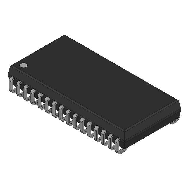
The CY7C1046CV33 is available in a standard 400-mil-wide
32-pin SOJ package with center power and ground (revolutionary) pinout.
Logic Block Diagram
Pin Configuration
SOJ
Top View
INPUT BUFFER
1M x 4
ARRAY
SENSE AMPS
I/O0
ROW DECODER
A0
A1
A2
A3
A4
A5
A6
A7
A8
A9
A10
A0
A1
A2
A3
A4
CE
I/O0
VCC
GND
I/O1
WE
A5
A6
A7
A8
A9
I/O1
I/O2
I/O3
COLUMN
DECODER
CE
POWER
DOWN
1
2
3
4
5
6
7
8
9
10
11
12
13
14
15
16
32
31
30
29
28
27
26
25
24
23
22
21
20
19
18
17
A19
A18
A17
A16
A15
OE
I/O3
GND
VCC
I/O2
A14
A13
A12
A11
A10
NC
OE
A 11
A 12
A 13
A14
A15
A16
A17
A18
A19
WE
Selection Guide
-8[2]
8
100
10
Maximum Access Time
Maximum Operating Current
Maximum CMOS Standby Current
-10
10
90
10
-12
12
85
10
-15
15
80
10
Unit
ns
mA
mA
Notes:
1. For guidelines on SRAM system design, please refer to the ‘System Design Guidelines’ Cypress application note, available on the internet at www.cypress.com.
2. Shaded areas contain advance information.
Cypress Semiconductor Corporation
Document Number: 38-05003 Rev. *B
•
3901 North First Street
•
San Jose
•
CA 95134 • 408-943-2600
Revised March 18, 2010
[+] Feedback
�CY7C1046CV33
Maximum Ratings
Current into Outputs (LOW)......................................... 20 mA
Static Discharge Voltage........................................... > 2001V
(per MIL-STD-883, Method 3015)
(Above which the useful life may be impaired. For user guidelines, not tested.)
Latch-up Current..................................................... > 200 mA
Storage Temperature ................................. –65C to +150C
Operating Range
Ambient Temperature with
Power Applied............................................. –55C to +125C
Supply Voltage on VCC to Relative GND[3] .... –0.5V to +4.6V
Range
Ambient
Temperature
VCC
DC Voltage Applied to Outputs
in High-Z State[3] ....................................–0.5V to VCC + 0.5V
Commercial
0C to +70C
3.0V – 3.6V
–40C to + 85C
3.0V – 3.6V
Industrial
DC Input Voltage[3] .................................–0.5V to VCC + 0.5V
DC Electrical Characteristics Over the Operating Range
-8[2]
Parameter
Description
Test Conditions
-10
-12
-15
Min. Max. Min. Max. Min. Max. Min. Max. Unit
VOH
Output HIGH Voltage VCC = Min., IOH = –4.0 mA
2.4
2.4
VOL
Output LOW Voltage VCC = Min., IOL = 8.0 mA
VIH
Input HIGH Voltage
2.0
VCC
+ 0.3
2.0
VCC
+ 0.3
2.0
VCC
+ 0.3
VIL
Input LOW Voltage[3]
–0.3
0.8
–0.3
0.8
–0.3
IIX
Input Load Current
GND < VI < VCC
–1
+1
–1
+1
IOZ
Output Leakage
Current
GND < VOUT < VCC,
Output Disabled
–1
+1
–1
+1
ICC
VCC Operating
Supply Current
VCC = Max.,
f = fMAX = 1/tRC
ISB1
ISB2
0.4
2.4
0.4
2.4
0.4
V
0.4
V
2.0
VCC
+ 0.3
V
0.8
–0.3
0.8
V
–1
+1
–1
+1
A
–1
+1
–1
+1
A
100
90
85
80
mA
Automatic CE
Max. VCC, CE > VIH
Power-Down Current VIN > VIH or
— TTL Inputs
VIN < VIL, f = fMAX
40
40
40
40
mA
Automatic CE
Max. VCC,
Commercial
Power-Down Current CE > VCC – 0.3V,
— CMOS Inputs
VIN > VCC – 0.3V,
or VIN < 0.3V,
f=0
10
10
10
10
mA
Capacitance[4]
Parameter
Description
CIN
Input Capacitance
COUT
I/O Capacitance
Test Conditions
TA = 25C, f = 1 MHz, VCC = 3.3V
Max.
Unit
6
pF
6
pF
Notes:
3. VIL (min.) = –2.0V for pulse durations of less than 20 ns.
4. Tested initially and after any design or process changes that may affect these parameters.
Document Number: 38-05003 Rev. *B
Page 2 of 9
[+] Feedback
�CY7C1046CV33
AC Test Loads and Waveforms[5]
8-, 10-ns devices:
12-, 15-ns devices:
Z=50
50
* CAPACITIVE LOAD CONSISTS
OF ALL COMPONENTS OF THE
TEST ENVIRONMENT
R 317
3.3V
OUTPUT
30 pF*
OUTPUT
R2
351
30 pF
1.5V
(b)
(a)
High-Z characteristics:
3.0V
GND
90%
90%
10%
Rise Time: 1 V/ns
10%
(c)
R 317
3.3V
ALL INPUT PULSES
Fall Time: 1 V/ns
OUTPUT
R2
351
5 pF
(d)
Notes:
5. AC characteristics (except High-Z) for all 8-ns and 10-ns parts are tested using the load conditions shown in Figure (a). All other speeds are tested using the
Thevenin load shown in Figure (b). High-Z characteristics are tested for all speeds using the test load shown in Figure (d).
Document Number: 38-05003 Rev. *B
Page 3 of 9
[+] Feedback
�CY7C1046CV33
AC Switching Characteristics[6] Over the Operating Range
-8[2]
Parameter
Description
Min.
-10
Max.
Min.
-12
Max.
Min.
-15
Max.
Min.
Max.
Unit
Read Cycle
tpower[7]
VCC(typical) to the first access
1
1
1
1
s
tRC
Read Cycle Time
8
10
12
15
ns
tAA
Address to Data Valid
tOHA
Data Hold from Address Change
tACE
CE LOW to Data Valid
8
10
12
15
ns
tDOE
OE LOW to Data Valid
4
5
6
7
ns
Low-Z[9]
tLZOE
OE LOW to
tHZOE
OE HIGH to High-Z[8, 9]
CE LOW to
Low-Z[9]
tHZCE
CE HIGH to
High-Z[8, 9]
tPU
CE LOW to Power-up
tPD
CE HIGH to Power-Down
tLZCE
Write
8
3
10
3
0
0
4
3
4
3
0
3
0
10
ns
7
6
ns
ns
7
0
12
ns
ns
0
6
5
8
15
3
0
5
3
0
12
3
ns
ns
15
ns
Cycle[10, 11]
tWC
Write Cycle Time
8
10
12
15
ns
tSCE
CE LOW to Write End
6
7
8
10
ns
tAW
Address Set-up to Write End
6
7
8
10
ns
tHA
Address Hold from Write End
0
0
0
0
ns
tSA
Address Set-up to Write Start
0
0
0
0
ns
tPWE
WE Pulse Width
6
7
8
10
ns
tSD
Data Set-up to Write End
4
5
6
7
ns
tHD
Data Hold from Write End
0
0
0
0
ns
3
3
3
3
ns
tLZWE
tHZWE
WE HIGH to
Low-Z[9]
WE LOW to
High-Z[8, 9]
4
5
6
7
ns
Notes:
6. Test conditions assume signal transition time of 3 ns or less, timing reference levels of 1.5V, input pulse levels of 0 to 3.0V.
7. tPOWER gives the minimum amount of time that the power supply should be at stable, typical Vcc values until the first memory access can be performed.
8. tHZOE, tHZCE, and tHZWE are specified with a load capacitance of 5 pF as in part (d) of AC Test Loads. Transition is measured 500 mV from steady-state voltage.
9. At any given temperature and voltage condition, tHZCE is less than tLZCE, tHZOE is less than tLZOE, and tHZWE is less than tLZWE for any given device.
10. The internal Write time of the memory is defined by the overlap of CE LOW, and WE LOW. CE and WE must be LOW to initiate a Write, and the transition of
either of these signals can terminate the Write. The input data set-up and hold timing should be referenced to the leading edge of the signal that terminates
the Write.
11. The minimum Write cycle time for Write Cycle no. 3 (WE controlled, OE LOW) is the sum of tHZWE and tSD.
Document Number: 38-05003 Rev. *B
Page 4 of 9
[+] Feedback
�CY7C1046CV33
Switching Waveforms
s
Read Cycle No. 1[14, 15]
tRC
ADDRESS
tOHA
DATA OUT
tAA
PREVIOUS DATA VALID
DATA VALID
Read Cycle No. 2 (OE Controlled)[15, 16]
ADDRESS
tRC
CE
tACE
OE
tHZOE
tDOE
DATA OUT
tLZOE
HIGH IMPEDANCE
tLZCE
VCC
SUPPLY
CURRENT
tHZCE
HIGH
IMPEDANCE
DATA VALID
tPD
tPU
50%
50%
ICC
ISB
Notes:
12. tr < 3 ns for the -10, -12, and -15 speeds.
13. No input may exceed VCC + 0.5V.
14. Device is continuously selected. OE, CE = VIL.
15. WE is HIGH for Read cycle.
16. Address valid prior to or coincident with CE transition LOW.
Document Number: 38-05003 Rev. *B
Page 5 of 9
[+] Feedback
�CY7C1046CV33
Switching Waveforms (continued)
Write Cycle No. 1 (CE Controlled)[17, 18]
tWC
ADDRESS
tSCE
CE
tSA
tSCE
tAW
tHA
tPWE
WE
tSD
DATA I/O
tHD
DATA VALID
Write Cycle No. 2 (WE Controlled, OE HIGH During Write)[17, 18]
tWC
ADDRESS
tSCE
CE
tAW
tSA
tHA
tPWE
WE
OE
tSD
DATA I/O
tHD
DATAIN VALID
NOTE 19
tHZOE
Notes:
17. Data I/O is high impedance if OE = VIH.
18. If CE goes HIGH simultaneously with WE going HIGH, the output remains in a high-impedance state.
19. During this period the I/Os are in the output state and input signals should not be applied.
Document Number: 38-05003 Rev. *B
Page 6 of 9
[+] Feedback
�CY7C1046CV33
Switching Waveforms (continued)
Write Cycle No. 3 (WE Controlled, OE LOW)[18]
tWC
ADDRESS
tSCE
CE
tAW
tSA
tHA
tPWE
WE
tSD
NOTE 19
DATA I/O
tHD
DATA VALID
tLZWE
tHZWE
Truth Table
CE
OE
WE
I/O0 – I/O7
Mode
Power
H
X
X
High-Z
Power-down
Standby (ISB)
L
L
H
Data Out
Read
Active (ICC)
L
X
L
Data In
Write
Active (ICC)
L
H
H
High-Z
Selected, Outputs Disabled
Active (ICC)
Ordering Information
Speed
(ns)
10
12
15
Ordering Code
Package
Name
Package Type
Operating
Range
CY7C1046CV33-10VC
V33
32-lead (400-mil) Molded SOJ
Commercial
CY7C1046CV33-10VI
V33
32-lead (400-mil) Molded SOJ
Industrial
CY7C1046CV33-12VC
V33
32-lead (400-mil) Molded SOJ
Commercial
CY7C1046CV33-12VI
V33
32-lead (400-mil) Molded SOJ
Industrial
CY7C1046CV33-15VC
V33
32-lead (400-mil) Molded SOJ
Commercial
CY7C1046CV33-15VI
V33
32-lead (400-mil) Molded SOJ
Industrial
Document Number: 38-05003 Rev. *B
Page 7 of 9
[+] Feedback
�CY7C1046CV33
Package Diagram
32-Lead (400-Mil) Molded SOJ V33
51-85033-*B
Document Number: 38-05003 Rev. *B
Page 8 of 9
[+] Feedback
�CY7C1046CV33
Document History Page
Document Title: CY7C1046CV33 1M x 4 Static RAM
Document Number: 38-05003
REV.
ECN NO.
SubmissionDate
Orig. of
Change
Description of Change
**
112570
03/06/02
HGK
New data sheet for RAM 7
*A
116478
09/16/02
CEA
Add applications foot note to data sheet, page 1.
*B
2895041
03/18/2010
AJU
Inactive part numbers; obsolete data sheet.
All product and company names mentioned in this document may be the trademarks of their respective holders.
Document Number: 38-05003 Rev. *B
Page 9 of 9
© Cypress Semiconductor Corporation, 2002-2010. The information contained herein is subject to change without notice. Cypress Semiconductor Corporation assumes no responsibility for the
use of any circuitry other than circuitry embodied in a Cypress Semiconductor product. Nor does it convey or imply any license under patent or other rights. Cypress Semiconductor does not
authorize its products for use as critical components in life-support systems where a malfunction or failure may reasonably be expected to result in significant injury to the user. The inclusion of
Cypress Semiconductor products in life-support systems application implies that the manufacturer assumes all risk of such use and in doing so indemnifies Cypress Semiconductor against all
charges.
[+] Feedback
�