CY7C1062AV25
512K x 32 Static RAM
Features
Functional Description
• High speed
The CY7C1062AV25 is a high-performance CMOS Static
RAM organized as 524,288 words by 32 bits.
— tAA = 10 ns
Writing to the device is accomplished by enabling the chip
(CE1, CE2 and CE3 LOW) and forcing the Write Enable (WE)
input LOW. If Byte Enable A (BA) is LOW, then data from I/O
pins (I/O0 through I/O7), is written into the location specified on
the address pins (A0 through A18). If Byte Enable B (BB) is
LOW, then data from I/O pins (I/O8 through I/O15) is written into
the location specified on the address pins (A0 through A18).
Likewise, BC and BD correspond with the I/O pins I/O16 to I/O23
and I/O24 to I/O31, respectively.
• Low active power
— 745 mW (max.)
• Operating voltages of 2.5 ± 0.2V
• 1.5V data retention
• Automatic power-down when deselected
• TTL-compatible inputs and outputs
• Easy memory expansion with CE1, CE2, and CE3
features
Reading from the device is accomplished by enabling the chip
(CE1, CE2, and CE3 LOW) while forcing the Output Enable
(OE) LOW and Write Enable (WE) HIGH. If the first Byte
Enable (BA) is LOW, then data from the memory location
specified by the address pins will appear on I/O0 to I/O7. If Byte
Enable B (BB) is LOW, then data from memory will appear on
I/O8 to I/O15. Similarly, Bc and BD correspond to the third and
fourth bytes. See the truth table at the back of this data sheet
for a complete description of read and write modes.
• Available in non Pb-free 119-ball pitch ball grid array
package
The input/output pins (I/O0 through I/O31) are placed in a
high-impedance state when the device is deselected (CE1,
CE2or CE3 HIGH), the outputs are disabled (OE HIGH), the
byte selects are disabled (BA-D HIGH), or during a write
operation (CE1, CE2, and CE3 LOW, and WE LOW).
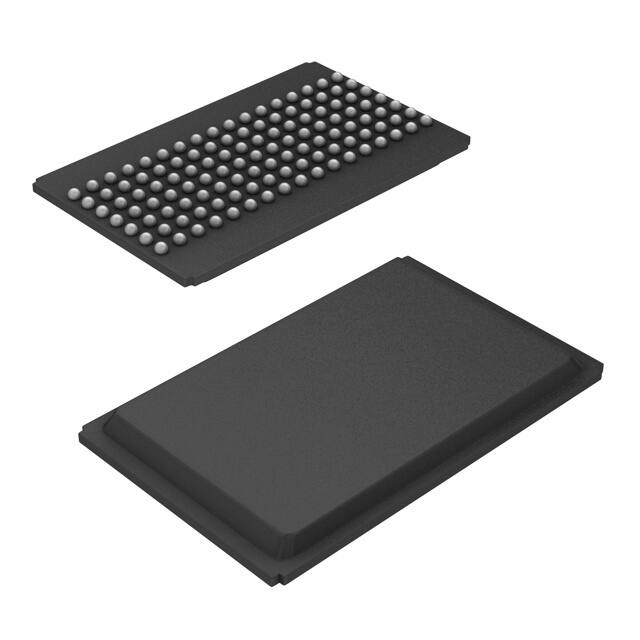
The CY7C1062AV25 is available in a 119-ball pitch ball grid
array (PBGA) package.
WE
CE1
CE2
CE3
OE
BA
BB
BC
BD
OUTPUT BUFFERS
512K x 32
ARRAY
SENSE AMPS
A0
A1
A2
A3
A4
A5
A6
A7
A8
A9
ROW DECODER
INPUT BUFFERS
CONTROL LOGIC
Logic Block Diagram
I/O0–I/O31
A 10
A 11
A 12
A 13
A 14
A 15
A 16
A 17
A 18
COLUMN
DECODER
Cypress Semiconductor Corporation
Document #: 38-05333 Rev. *A
•
198 Champion Court
•
San Jose, CA 95134-1709
•
408-943-2600
Revised July 10, 2006
�CY7C1062AV25
Selection Guide
–10
Maximum Access Time
Unit
10
ns
Maximum Operating Current
Com’l/Ind’l
275
mA
Maximum CMOS Standby Current
Com’l/Ind’l
50
mA
Pin Configuration
119-ball PBGA
(Top View)
1
2
3
4
5
6
7
A
I/O16
A
A
A
A
A
I/O0
B
C
D
E
F
G
H
J
K
L
M
N
P
I/O17
I/O18
I/O19
A
Bc
VDD
A
CE2
VSS
CE1
NC
VSS
A
CE3
VSS
A
Ba
VDD
I/O1
I/O2
I/O3
I/O20
VSS
VDD
VSS
VDD
VSS
I/O4
I/O21
VDD
VSS
VSS
VSS
VDD
I/O5
I/O22
VSS
VDD
VSS
VDD
VSS
I/O6
I/O23
NC
VDD
VSS
VSS
VDD
VSS
VSS
VSS
VDD
VDD
VSS
I/O7
DNU
I/O24
I/O25
VDD
VSS
VSS
VDD
VSS
VSS
VSS
VDD
VDD
VSS
I/O8
I/O9
I/O10
R
T
U
Document #: 38-05333 Rev. *A
I/O26
VDD
VSS
VSS
VSS
VDD
I/O27
VSS
VDD
VSS
VDD
VSS
I/O11
I/O28
VDD
VSS
VSS
VSS
VDD
I/O12
I/O29
A
Bd
NC
Bb
A
I/O13
I/O30
A
A
WE
A
A
I/O14
I/O31
A
A
OE
A
A
I/O15
Page 2 of 9
�CY7C1062AV25
Maximum Ratings
Current into Outputs (LOW)......................................... 20 mA
(Above which the useful life may be impaired. For user guidelines, not tested.)
Static Discharge Voltage............................................ >2001V
(per MIL-STD-883, Method 3015)
Storage Temperature ................................. –65°C to +150°C
Latch-up Current...................................................... >200 mA
Ambient Temperature with
Power Applied............................................. –55°C to +125°C
Operating Range
Supply Voltage on VCC Relative to GND
[1]
DC Voltage Applied to Outputs
in High-Z State[1] ....................................–0.5V to VCC + 0.5V
.... –0.5V to +3.6V
Range
Ambient
Temperature
VCC
Commercial
0°C to +70°C
2.5V ± 0.2V
DC Input Voltage[1] .................................–0.5V to VCC + 0.5V
Industrial
–40°C to +85°C
DC Electrical Characteristics Over the Operating Range
–10
Parameter
Description
Test Conditions
VOH
Output HIGH Voltage
VCC = Min., IOH = –1.0 mA
VOL
Output LOW Voltage
VCC = Min., IOL = 1.0 mA
Min.
Max.
Unit
2.0
V
0.4
V
VIH
Input HIGH Voltage
2.0
VCC + 0.3
V
VIL
Input LOW Voltage[1]
–0.3
0.8
V
IIX
Input Leakage Current
GND < VI < VCC
–1
+1
µA
IOZ
Output Leakage Current
GND < VOUT < VCC, Output Disabled
–1
+1
µA
ICC
VCC Operating
Supply Current
VCC = Max., f = fMAX = 1/tRC
Com’l/Ind’l
275
mA
ISB1
Automatic CE Power-down
Current—TTL Inputs
Max. VCC, CE > VIH, VIN > VIH or
VIN < VIL, f = fMAX
Com’l/Ind’l
100
mA
ISB2
Automatic CE Power-down
Current —CMOS Inputs
Max. VCC, CE > VCC – 0.2V,
Com’l/Ind’l
VIN > VCC – 0.2V, or VIN < 0.2V, f = 0
50
mA
Capacitance[2]
Parameter
Description
CIN
Input Capacitance
COUT
I/O Capacitance
Test Conditions
TA = 25°C, f = 1 MHz, VCC = 2.5V
Max.
Unit
8
pF
10
pF
AC Test Loads and Waveforms[3]
50Ω
VTH = VDD/2
OUTPUT
Z0 = 50Ω
(a)
2.5V
Including OUTPUT
Jig and
Scope
30 pF
Including all Components
R1 317Ω of Test Equipment
5 pF
(b)
R2
351Ω
ALL INPUT PULSES
2.3V
90%
90%
10%
10%
GND
Fall time:
> 1 V/ns
Rise time > 1 V/ns
THÉVENIN EQUIVALENT
167Ω
OUTPUT
1.73V
(c)
Notes:
1. VIL (min.) = –2.0V for pulse durations of less than 20 ns.
2. Tested initially and after any design or process changes that may affect these parameters.
3. Valid SRAM operation does not occur until the power supplies have reached the minimum operating VDD (2.3V). As soon as 1ms (Tpower) after reaching the
minimum operating VDD, normal SRAM operation can begin including reduction in VDD to the data retention (VCCDR, 1.5V) voltage.
Document #: 38-05333 Rev. *A
Page 3 of 9
�CY7C1062AV25
AC Switching Characteristics Over the Operating Range[4]
–10
Parameter
Description
Min.
Max.
Unit
Read Cycle
tpower
VCC (typical) to the first access[5]
1
ms
tRC
Read Cycle Time
10
ns
tAA
Address to Data Valid
tOHA
Data Hold from Address Change
tACE
CE1, CE2, or CE3 LOW to Data Valid
10
ns
tDOE
OE LOW to Data Valid
5
ns
tLZOE
OE LOW to Low-Z
10
[6]
OE HIGH to High-Z
tLZCE
CE1, CE2, or CE3 LOW to Low-Z[6]
CE1, CE2, or CE3 HIGH to
CE1, CE2, or CE3 LOW to
Power-up[7]
tPD
CE1, CE2, or CE3 HIGH to
Power-down[7]
tDBE
Byte Enable to Data Valid
tPU
tLZBE
tHZBE
Byte Enable to
Low-Z[6]
Byte Disable to
High-Z[6]
ns
5
High-Z[6]
tHZCE
ns
1
[6]
tHZOE
Write
3
ns
3
ns
ns
5
0
ns
ns
10
ns
5
ns
1
ns
5
ns
Cycle[8, 9]
tWC
Write Cycle Time
10
ns
tSCE
CE1, CE2, or CE3 LOW to Write End
7
ns
tAW
Address Set-up to Write End
7
ns
tHA
Address Hold from Write End
0
ns
tSA
Address Set-up to Write Start
0
ns
tPWE
WE Pulse Width
7
ns
tSD
Data Set-up to Write End
5.5
ns
tHD
Data Hold from Write End
0
ns
tLZWE
WE HIGH to Low-Z[6]
3
ns
tHZWE
WE LOW to High-Z
[6]
tBW
Byte Enable to End of Write
5
7
ns
ns
Notes:
4. Test conditions assume signal transition time of 3 ns or less, timing reference levels of 1.1V, input pulse levels of 0 to 2.3V, and output loading of the specified
IOL/IOH and transmission line loads. Test conditions for the read cycle use output loading as shown in (a) of AC Test Loads, unless specified otherwise.
5. This part has a voltage regulator that steps down the voltage from 2.3V to 2V internally. tpower time has to be provided initially before a read/write operation is
started.
6. tHZOE, tHZCE, tHZWE, tHZBE, and tLZOE, tLZCE, tLZWE, and tLZBE are specified with a load capacitance of 5 pF as in (b) of AC Test Loads. Transition is measured
± 200 mV from steady-state voltage.
7. These parameters are guaranteed by design and are not tested.
8. The internal write time of the memory is defined by the overlap of CE1 LOW, CE 2 HIGH, CE3 LOW, and WE LOW. The chip enables must be active and WE
must be LOW to initiate a write, and the transition of any of these signals can terminate the write. The input data set-up and hold timing should be referenced
to the leading edge of the signal that terminates the write.
9. The minimum write cycle time for Write Cycle No. 3 (WE controlled, OE LOW) is the sum of tHZWE and tSD.
Document #: 38-05333 Rev. *A
Page 4 of 9
�CY7C1062AV25
Data Retention Waveform
DATA RETENTION MODE
2.3V
VCC
2.3V
VDR > 1.5V
tR
tCDR
CE
Switching Waveforms
Read Cycle No. 1[11,12]
tRC
ADDRESS
tAA
tOHA
DATA OUT
PREVIOUS DATA VALID
DATA VALID
Read Cycle No. 2 (OE Controlled)[11,13]
ADDRESS
tRC
CE1, CE3
CE2
tACE
OE
tHZOE
tDOE
tLZOE
BA, BB, BC , BD
tHZCE
tDBE
tLZBE
DATA OUT
HIGH IMPEDANCE
tHZBE
DATA VALID
tLZCE
VCC
SUPPLY
CURRENT
HIGH
IMPEDANCE
tPD
tPU
50%
IICC
CC
50%
ISB
Notes:
10. Full device operation requires linear VCC ramp from VDR to VCC(min.) > 100 µs or stable at VCC(min.) > 100 µs
11. Device is continuously selected. OE, CE, BA, BB, BC, BD= VIL.
12. WE is HIGH for read cycle.
13. Address valid prior to or coincident with CE transition LOW.
Document #: 38-05333 Rev. *A
Page 5 of 9
�CY7C1062AV25
Switching Waveforms
Write Cycle No. 1 (CE Controlled)[14,15,16]
tWC
ADDRESS
CE
tSA
tSCE
tAW
tHA
tPWE
WE
tBW
BA, BB, BC , BD
tSD
tHD
DATAI/O
Write Cycle No. 2 (BLE or BHE Controlled)[14,15,16]
tWC
ADDRESS
tSA
tBW
BA, BB, BC , BD
tAW
tHA
tPWE
WE
tSCE
CE
tSD
tHD
DATAI/O
Notes:
14. CE indicates a combination of all three chip enables. When ACTIVE LOW, CE indicates the CE1, CE2 and CE3 are LOW.
15. Data I/O is high-impedance if OE or BA, BB, BC, BD = VIH.
16. If CE goes HIGH simultaneously with WE going HIGH, the output remains in a high-impedance state.
Document #: 38-05333 Rev. *A
Page 6 of 9
�CY7C1062AV25
Switching Waveforms
Write Cycle No. 3 (WE Controlled, OE LOW)
tWC
ADDRESS
tSCE
CE
tAW
tHA
tSA
tPWE
WE
tBW
BA, BB, BC, BD
tHZWE
tSD
tHD
DATA I/O
tLZWE
Truth Table
CE1 CE2 CE3
I/O0–
I/O7
I/O8–
I/O15
I/O16–
I/O23
I/O24–
I/O31
OE
WE
BA
BB
Bc
BD
X
X
X
X
X
High-Z
High-Z
High-Z
High-Z
Power Down
Mode
(ISB)
Power
H
H
H
X
L
H
L
X
X
X
X
X
X
High-Z
High-Z
High-Z
High-Z
Power Down
(ISB)
L
L
L
L
H
L
L
L
L
Data Out
Data Out
Data Out
Data Out
Read All Bits
(ICC)
L
L
L
L
H
L
H
H
H
Data Out
High-Z
High-Z
High-Z
Read Byte A
Bits Only
(ICC)
L
L
L
L
H
H
L
H
H
High-Z
Data Out
High-Z
High-Z
Read Byte B
Bits Only
(ICC)
L
L
L
L
H
H
H
L
H
High-Z
High-Z
Data Out
High-Z
Read Byte C
Bits Only
(ICC)
L
L
L
L
H
H
H
H
L
High-Z
High-Z
High-Z
Data Out
Read Byte D
Bits Only
(ICC)
L
L
L
X
L
L
L
L
L
Data In
Data In
Data In
Data In
Write All Bits
(ICC)
L
L
L
X
L
L
H
H
H
Data In
High-Z
High-Z
High-Z
Write Byte A
Bits Only
(ICC)
L
L
L
X
L
H
L
H
H
High-Z
Data In
High-Z
High-Z
Write Byte B
Bits Only
(ICC)
L
L
L
X
L
H
H
L
H
High-Z
High-Z
Data In
High-Z
Write Byte C
Bits Only
(ICC)
L
L
L
X
L
H
H
H
L
High-Z
High-Z
High-Z
Data In
Write Byte D
Bits Only
(ICC)
L
L
L
H
H
X
X
X
X
High-Z
High-Z
High-Z
High-Z
Selected,
Outputs
Disabled
(ICC)
Document #: 38-05333 Rev. *A
Page 7 of 9
�CY7C1062AV25
Ordering Information
Speed
(ns)
10
Ordering Code
CY7C1062AV25-10BGC
CY7C1062AV25-10BGI
Package
Diagram
51-85115
Operating
Range
Commercial
Industrial
Package Type
119-ball Plastic Ball Grid Array (14 x 22 x 2.4 mm)
Package Diagram
119-ball PBGA (14 x 22 x 2.4 mm) (51-85115)
51-85115-*B
All product and company names mentioned in this document may be the trademarks of their respective holders.
Document #: 38-05333 Rev. *A
Page 8 of 9
�CY7C1062AV25
Document History Page
Document Title: CY7C1062AV25 512K x 32 Static RAM
Document Number: 38-05333
REV.
ECN NO.
Issue
Date
Orig. of
Change
Description of Change
**
119626
01/29/03
DFP
New Data Sheet
*A
493565
See ECN
NXR
Converted from Preliminary to Final
Removed -8 and -10 speed bins
Changed the description of IIX from Input Load Current to Input Leakage
Current in DC Electrical Characteristics table
Updated the ordering information table
Document #: 38-05333 Rev. *A
Page 9 of 9
�


 工商网监
湘ICP备2023018690号
工商网监
湘ICP备2023018690号
