CY7C1069DV33-10BVXIKA 数据手册
THIS SPEC IS OBSOLETE
Spec No:
38-05478
Spec Title:
CY7C1069DV33, 16-MBIT (2M X 8) STATIC RAM
Replaced by:
None
�CY7C1069DV33
16-Mbit (2M × 8) Static RAM
16-Mbit (2M × 8) Static RAM
Features
Functional Description
■
High speed
❐ tAA = 10 ns
The CY7C1069DV33 is a high performance CMOS Static RAM
organized as 2,097,152 words by 8 bits.
■
Low active power
❐ ICC = 175 mA at 100 MHz
■
Low complementary metal oxide semiconductor (CMOS)
standby power
❐ ISB2 = 25 mA
To write to the device, take Chip Enables (CE1 LOW and CE2
HIGH) and Write Enable (WE) input LOW. Data on the eight I/O
pins (I/O0 through I/O7) is then written into the location specified
on the address pins (A0 through A20).
■
Operating voltages of 3.3 ± 0.3 V
■
2.0 V data retention
■
Automatic power-down when deselected
■
Transistor-transistor logic (TTL) compatible inputs and outputs
■
Easy memory expansion with CE1 and CE2 features
■
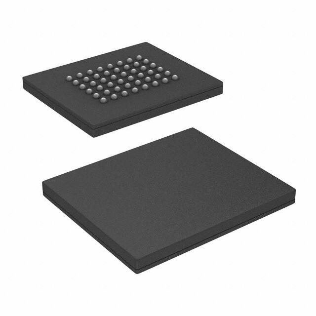
Available in Pb-free 54-pin thin small outline package (TSOP)
Type II and 48-ball very fine-pitch ball grid array (VFBGA)
packages.
To read from the device, take Chip Enables (CE1 LOW and CE2
HIGH) and Output Enable (OE) LOW while forcing the Write
Enable (WE) HIGH. Under these conditions, the contents of the
memory location specified by the address pins will appear on the
I/O pins. See Truth Table on page 10 for a complete description
of Read and Write modes.
The input and output pins (I/O0 through I/O7) are placed in a high
impedance state when the device is deselected (CE1 HIGH or
CE2 LOW), the outputs are disabled (OE HIGH), or during a write
operation (CE1 LOW, CE2 HIGH, and WE LOW).
The CY7C1069DV33 is available in a 54-pin TSOP II package
with center power and ground (revolutionary) pinout, and a
48-ball very fine-pitch ball grid array (VFBGA) package.
For a complete list of related documentation, click here.
Logic Block Diagram
2M x 8
ARRAY
SENSE AMPS
A0
A1
A2
A3
A4
A5
A6
A7
A8
A9
ROW DECODER
INPUT BUFFER
I/O0 – I/O7
WE
CE2
OE
COLUMN
DECODER
A10
A11
A 12
A 13
A 14
A15
A16
A17
A18
A19
A20
CE1
Cypress Semiconductor Corporation
Document Number: 38-05478 Rev. *J
•
198 Champion Court
•
San Jose, CA 95134-1709
•
408-943-2600
Revised November 22, 2016
�CY7C1069DV33
Contents
Selection Guide ................................................................ 3
Pin Configurations ........................................................... 3
Maximum Ratings ............................................................. 4
Operating Range ............................................................... 4
DC Electrical Characteristics .......................................... 4
Capacitance ...................................................................... 5
Thermal Resistance .......................................................... 5
AC Test Loads and Waveforms ....................................... 5
Data Retention Characteristics ....................................... 6
Data Retention Waveform ................................................ 6
AC Switching Characteristics ......................................... 7
Switching Waveforms ...................................................... 8
Truth Table ...................................................................... 10
Document Number: 38-05478 Rev. *J
Ordering Information ...................................................... 10
Ordering Code Definitions ......................................... 10
Package Diagrams .......................................................... 11
Acronyms ........................................................................ 13
Document Conventions ................................................. 13
Units of Measure ....................................................... 13
Document History Page ................................................. 14
Sales, Solutions, and Legal Information ...................... 15
Worldwide Sales and Design Support ....................... 15
Products .................................................................... 15
PSoC®Solutions ....................................................... 15
Cypress Developer Community ................................. 15
Technical Support ..................................................... 15
Page 2 of 15
�CY7C1069DV33
Selection Guide
-10
Unit
Maximum access time
10
ns
Maximum operating current
175
mA
Maximum CMOS standby current
25
mA
Pin Configurations
Figure 1. 54-pin TSOP II pinout (Top View) [1]
NC
VCC
NC
I/O6
VSS
I/O7
A4
A3
A2
A1
A0
NC
CE1
VCC
WE
CE2
A19
A18
A17
A16
A15
I/O0
VCC
I/O1
NC
VSS
NC
1
2
3
4
5
6
7
8
9
10
11
12
13
14
15
16
17
18
19
20
21
22
23
24
25
26
27
45
44
NC
VSS
NC
I/O5
VCC
I/O4
A5
A6
A7
A8
A9
43
42
41
40
39
38
37
36
35
34
33
32
31
30
29
28
NC
OE
VSS
NC
A20
A10
A11
A12
A13
A14
I/O3
VSS
I/O2
NC
VCC
NC
54
53
52
51
50
49
48
47
46
Figure 2. 48-ball VFBGA pinout (Top View) [1]
1
2
3
4
5
6
NC
OE
A0
A1
A2
CE2
A
NC
NC
A3
A4
CE1
NC
B
I/O0
NC
A5
A6
NC
I/O4
C
VSS
I/O1
A17
A7
I/O5
VCC
D
VCC
I/O2
A18
A16
I/O6
VSS
E
I/O3
NC
A14
A15
NC
I/O7
F
NC
NC
A12
A13
WE
NC
G
A19
A8
A9
A10
A11
A20
H
Note
1. NC pins are not connected on the die.
Document Number: 38-05478 Rev. *J
Page 3 of 15
�CY7C1069DV33
DC input voltage [2] ............................. –0.5 V to VCC + 0.5 V
Maximum Ratings
Exceeding maximum ratings may shorten the useful life of the
device. These user guidelines are not tested.
Storage temperature ................................ –65 C to +150 C
Ambient temperature
with power applied ................................... –55 C to +125 C
Current into outputs (LOW) ........................................ 20 mA
Static discharge voltage
(MIL-STD-883, method 3015) ................................. > 2001 V
Latch-up current .................................................... > 200 mA
Operating Range
Supply voltage
on VCC relative to GND [2] ...........................–0.5 V to +4.6 V
DC voltage applied to outputs
in High Z state [2] ................................ –0.5 V to VCC + 0.5 V
Range
Ambient Temperature
VCC
Industrial
–40 C to +85 C
3.3 V 0.3 V
DC Electrical Characteristics
Over the Operating Range
Parameter
Description
Test Conditions
-10
Unit
Min
Max
2.4
–
V
VOH
Output HIGH voltage
Min VCC, IOH = –4.0 mA
VOL
Output LOW voltage
Min VCC, IOL = 8.0 mA
–
0.4
V
VIH
Input HIGH voltage
–
2.0
VCC + 0.3
V
–
–0.3
0.8
V
+1
A
[2]
VIL
Input LOW voltage
IIX
Input leakage current
GND < VIN < VCC
–1
IOZ
Output leakage current
GND < VOUT < VCC, Output disabled
–1
+1
A
ICC
VCC operating supply current
VCC = Max, f = fMAX = 1/tRC, IOUT = 0 mA,
CMOS levels
–
175
mA
ISB1
Automatic CE power-down
current – TTL inputs
Max VCC, CE1 > VIH, CE2 < VIL,
VIN > VIH or VIN < VIL, f = fMAX
–
30
mA
ISB2
Automatic CE power-down
current – CMOS inputs
Max VCC, CE1 > VCC – 0.3 V, CE2 < 0.3 V,
VIN > VCC – 0.3 V or VIN < 0.3 V, f = 0
–
25
mA
Note
2. VIL(min) = –2.0 V and VIH(max) = VCC + 2 V for pulse durations of less than 20 ns.
Document Number: 38-05478 Rev. *J
Page 4 of 15
�CY7C1069DV33
Capacitance
Parameter [3]
Description
CIN
Input capacitance
COUT
IO capacitance
Test Conditions
TSOP II
VFBGA
Unit
6
8
pF
8
10
pF
TSOP II
VFBGA
Unit
76.15
28.37
C/W
14.15
5.79
C/W
High Z characteristics
3.3 V
R1 317
TA = 25 C, f = 1 MHz, VCC = 3.3 V
Thermal Resistance
Parameter [3]
Description
JA
Thermal resistance
(junction to ambient)
JC
Thermal resistance
(junction to case)
Test Conditions
Still air, soldered on a 3 × 4.5 inch, four
layer printed circuit board
AC Test Loads and Waveforms
Figure 3. AC Test Loads and Waveforms [4]
50
VTH = 1.5 V
OUTPUT
Z0 = 50
OUTPUT
30 pF*
5 pF*
(a)
* Capacitive load consists
of all components of the
test environment
3.0 V
GND
Rise Time > 1 V/ns
ALL INPUT PULSES
90%
90%
10%
10%
(c)
R2
351
INCLUDING
JIG AND
SCOPE
(b)
Fall Time:
> 1 V/ns
Notes
3. Tested initially and after any design or process changes that may affect these parameters.
4. Valid SRAM operation does not occur until the power supplies have reached the minimum operating VDD (3.0 V). 100 s (tpower) after reaching the minimum operating
VDD, normal SRAM operation begins including reduction in VDD to the data retention (VCCDR, 2.0 V) voltage.
Document Number: 38-05478 Rev. *J
Page 5 of 15
�CY7C1069DV33
Data Retention Characteristics
Over the Operating Range
Parameter
Description
Conditions
VDR
VCC for data retention
ICCDR
Data retention current
tCDR [5]
Chip deselect to data retention
time
tR [6]
Operation recovery time
VCC = 2 V, CE1 > VCC – 0.2 V, CE2 < 0.2 V,
VIN > VCC – 0.2 V or VIN < 0.2 V
Min
Max
Unit
2
–
V
25
mA
0
–
ns
tRC
–
ns
–
Data Retention Waveform
Figure 4. Data Retention Waveform
DATA RETENTION MODE
VCC
3.0 V
VDR > 2 V
tCDR
3.0 V
tR
CE
Notes
5. Tested initially and after any design or process changes that may affect these parameters.
6. Full device operation requires linear VCC ramp from VDR to VCC(min) > 50 s or stable at VCC(min) > 50 s.
Document Number: 38-05478 Rev. *J
Page 6 of 15
�CY7C1069DV33
AC Switching Characteristics
Over the Operating Range
Parameter [7]
Description
-10
Min
Max
Unit
Read Cycle
tpower
VCC(typical) to the first access [8]
100
–
s
tRC
Read cycle time
10
–
ns
tAA
Address to data valid
–
10
ns
tOHA
Data hold from address change
3
–
ns
tACE
CE1 LOW/CE2 HIGH to data valid
–
10
ns
tDOE
OE LOW to data valid
–
5
ns
1
–
ns
–
5
ns
3
–
ns
–
5
ns
0
–
ns
–
10
ns
tLZOE
OE LOW to low Z
[9]
[9]
tHZOE
OE HIGH to high Z
tLZCE
CE1 LOW/CE2 HIGH to low Z [9]
tHZCE
tPU
tPD
CE1 HIGH/CE2 LOW to high Z
[9]
CE1 LOW/CE2 HIGH to power-up
[10]
CE1 HIGH/CE2 LOW to power-down
[10]
Write Cycle [11, 12]
tWC
Write cycle time
10
–
ns
tSCE
CE1 LOW/CE2 HIGH to write end
7
–
ns
tAW
Address setup to write end
7
–
ns
tHA
Address hold from write end
0
–
ns
tSA
Address setup to write start
0
–
ns
tPWE
WE pulse width
7
–
ns
tSD
Data setup to write end
5.5
–
ns
tHD
Data hold from write end
0
–
ns
WE HIGH to low Z
[9]
3
–
ns
WE LOW to high Z
[9]
–
5
ns
tLZWE
tHZWE
Notes
7. Test conditions assume signal transition time of 3 ns or less, timing reference levels of 1.5 V, and input pulse levels of 0 to 3.0 V. Test conditions for the read cycle use
output loading shown in (a) of Figure 3 on page 5, unless specified otherwise.
8. tPOWER gives the minimum amount of time that the power supply is at typical VCC values until the first memory access is performed.
9. tHZOE, tHZCE, tHZWE, tLZOE, tLZCE, and tLZWE are specified with a load capacitance of 5 pF as in (b) of Figure 3 on page 5. Transition is measured 200 mV from steady state voltage.
10. These parameters are guaranteed by design and are not tested.
11. The internal write time of the memory is defined by the overlap of WE, CE1 = VIL, and CE2 = VIH. CE1 and WE are LOW along with CE2 HIGH to initiate a write, and the
transition of any of these signals can terminate. The input data setup and hold timing should be referenced to the edge of the signal that terminates the write.
12. The minimum write cycle time for Write Cycle No. 2 (WE Controlled, OE LOW) is the sum of tHZWE and tSD.
Document Number: 38-05478 Rev. *J
Page 7 of 15
�CY7C1069DV33
Switching Waveforms
Figure 5. Read Cycle No. 1 (Address Transition Controlled) [13, 14]
tRC
RC
ADDRESS
tOHA
DATA I/O
tAA
PREVIOUS DATA VALID
DATA OUT VALID
Figure 6. Read Cycle No. 2 (OE Controlled) [14, 15]
ADDRESS
tRC
CE1
CE2
tACE
OE
tHZOE
tDOE
tHZCE
tLZOE
DATA I/O
HIGH IMPEDANCE
tLZCE
VCC
SUPPLY
CURRENT
HIGH
IMPEDANCE
DATA OUT VALID
tPD
tPU
50%
50%
ICC
ISB
Notes
13. The device is continuously selected. CE1 = VIL, and CE2 = VIH.
14. WE is HIGH for read cycle.
15. Address valid before or similar to CE1 transition LOW and CE2 transition HIGH.
Document Number: 38-05478 Rev. *J
Page 8 of 15
�CY7C1069DV33
Switching Waveforms (continued)
Figure 7. Write Cycle No. 1 (CE Controlled) [16, 17, 18]
tWC
ADDRESS
tSA
CE
tSCE
tAW
tHA
tPWE
WE
tSD
tHD
DATA IN VALID
DATA IO
Figure 8. Write Cycle No. 2 (WE Controlled, OE LOW) [16, 17, 18, 19]
tWC
ADDRESS
tSCE
CE
tAW
tHA
tSA
tPWE
WE
tHZWE
DATA I/O
tSD
tHD
DATA IN VALID
tLZWE
Notes
16. CE is a shorthand combination of both CE1 and CE2 combined. It is active LOW.
17. Data I/O is high impedance if OE = VIH.
18. If CE goes HIGH simultaneously with WE going HIGH, the output remains in a high impedance state.
19. The minimum write cycle time is the sum of tHZWE and tSD.
Document Number: 38-05478 Rev. *J
Page 9 of 15
�CY7C1069DV33
Truth Table
CE1
CE2
OE
WE
I/O0–I/O7
Mode
Power
H
X
X
X
High Z
Power-down
Standby (ISB)
X
L
X
X
High Z
Power-down
Standby (ISB)
L
H
L
H
Data out
Read all bits
Active (ICC)
L
H
X
L
Data in
Write all bits
Active (ICC)
L
H
H
H
High Z
Selected, outputs disabled
Active (ICC)
Ordering Information
Speed
(ns)
10
Ordering Code
Package
Diagram
Package Type
CY7C1069DV33-10ZSXI
51-85160 54-pin TSOP II (Pb-free)
CY7C1069DV33-10BVXI
51-85178 48-ball VFBGA (Pb-free)
Operating
Range
Industrial
Ordering Code Definitions
CY 7 C 1 06 9
D V33 - 10 XX X
I
Temperature Range:
I = Industrial
Pb-free
Package Type: XX = ZS or BV
ZS = 54-pin TSOP II
BV = 48-ball VFBGA
Speed: 10 ns
Voltage Range: V33 = 3 V to 3.6 V
Process Technology: D = C9, 90 nm
Data Width: 9 = × 8-bits
Density: 06 = 16-Mbit density
Family Code: 1 = Fast Asynchronous SRAM family
Technology Code: C = CMOS
Marketing Code: 7 = SRAM
Company ID: CY = Cypress
Document Number: 38-05478 Rev. *J
Page 10 of 15
�CY7C1069DV33
Package Diagrams
Figure 9. 54-pin TSOP Type II (22.4 × 11.84 × 1.0 mm) Z54-II Package Outline, 51-85160
51-85160 *E
Document Number: 38-05478 Rev. *J
Page 11 of 15
�CY7C1069DV33
Package Diagrams (continued)
Figure 10. 48-ball VFBGA (8 × 9.5 × 1.0 mm) VCG048/BZ48B Package Outline, 51-85178
2X
0.10 C
E1
E
B
6
5
4
3
2
A1 CORNER
(datum B)
1
7
A1 CORNER
A
6
B
SD
C
D
D
E
D1
(datum A)
F
G
H
eD
0.10 C 2X
eE
6
A
TOP VIEW
SE
BOTTOM VIEW
0.25 C
A1
0.10 C
C
48XØb
DETAIL A
A
5
Ø0.05 M C A B
Ø0.25 M C
DETAIL A
SIDE VIEW
NOTES:
1. ALL DIMENSIONS ARE IN MILLIMETERS.
DIMENSIONS
SYMBOL
MIN.
NOM.
MAX.
2. SOLDER BALL POSITION DESIGNATION PER JEP95, SECTION 3, SPP-020.
A
-
-
1.00
3. "e" REPRESENTS THE SOLDER BALL GRID PITCH.
A1
0.16
0.21
0.26
4. SYMBOL "MD" IS THE BALL MATRIX SIZE IN THE "D" DIRECTION.
D
9.50 BSC
E
8.00 BSC
D1
5.25 BSC
E1
3.75 BSC
MD
N IS THE NUMBER OF POPULATED SOLDER BALL POSITIONS FOR MATRIX
SIZE MD X ME.
5. DIMENSION "b" IS MEASURED AT THE MAXIMUM BALL DIAMETER IN A
PLANE PARALLEL TO DATUM C.
8
ME
6
N
48
b
SYMBOL "ME" IS THE BALL MATRIX SIZE IN THE "E" DIRECTION.
0.25
0.30
eD
0.75 BSC
eE
0.75 BSC
SD
0.38
SE
0.38
6. "SD" AND "SE" ARE MEASURED WITH RESPECT TO DATUMS A AND B AND
DEFINE THE POSITION OF THE CENTER SOLDER BALL IN THE OUTER ROW.
0.35
WHEN THERE IS AN ODD NUMBER OF SOLDER BALLS IN THE OUTER ROW,
"SD" OR "SE" = 0.
WHEN THERE IS AN EVEN NUMBER OF SOLDER BALLS IN THE OUTER ROW,
"SD" = eD/2 AND "SE" = eE/2.
7. A1 CORNER TO BE IDENTIFIED BY CHAMFER, LASER OR INK MARK
METALIZED MARK, INDENTATION OR OTHER MEANS.
8. "+" INDICATES THE THEORETICAL CENTER OF DEPOPULATED SOLDER
BALLS.
51-85178 *D
Document Number: 38-05478 Rev. *J
Page 12 of 15
�CY7C1069DV33
Acronyms
Acronym
Document Conventions
Description
Units of Measure
CE
chip enable
CMOS
complementary metal oxide semiconductor
°C
degree Celsius
I/O
input/output
MHz
megahertz
OE
output enable
A
microampere
SRAM
static random access memory
s
microsecond
VFBGA
very fine-pitch ball grid array
mA
milliampere
TSOP
thin small outline package
ns
nanosecond
TTL
transistor-transistor logic
ohm
WE
write enable
%
percent
pF
picofarad
V
volt
W
watt
Document Number: 38-05478 Rev. *J
Symbol
Unit of Measure
Page 13 of 15
�CY7C1069DV33
Document History Page
Document Title: CY7C1069DV33, 16-Mbit (2M × 8) Static RAM
Document Number: 38-05478
Rev.
ECN No.
Issue Date
Orig. of
Change
**
201560
See ECN
SWI
Advance datasheet for C9 IPP
*A
233748
See ECN
RKF
Modified AC, DC parameters as per EROS (Specification 01-2165)
Pb-free Offering in the Ordering Information
*B
469420
See ECN
NXR
Changed status from Advance Information to Preliminary.
Removed -8 and -12 speed bins from product offering
Removed Commercial Operating Range
Changed 2G Ball of FBGA and pin 40 of TSOPII from DNU to NC
Included the Maximum ratings for Static Discharge Voltage and Latch Up
Current on page 3
Changed ICC(Max) from 220 mA to 100 mA
Changed ISB1(Max) from 70 mA to 30 mA
Changed ISB2(Max) from 40 mA to 25 mA
Specified the Overshoot specification in footnote 1
Added Data Retention Characteristics table on page 5
Updated the 48-pin FBGA package
Updated the Ordering Information table.
*C
499604
See ECN
NXR
Added note 1 for NC pins
Updated Test Condition for ICC in DC Electrical Characteristics table
Updated the 48-ball FBGA Package
*D
1462585
See ECN
VKN /
AESA
Changed status from Preliminary to Final.
Updated DC Electrical Characteristics:
Changed maximum value of ICC parameter from 125 mA to 175 mA.
Updated Thermal Resistance.
*E
3109063
12/13/2010
AJU
*F
3147335
01/19/2011
PRAS
Added Acronyms and Units of Measure.
Updated to new template.
*G
3417274
10/21/2011
TAVA
Updated Features.
Updated DC Electrical Characteristics.
Updated Switching Waveforms.
*H
4575167
11/19/2014
TAVA
Updated Functional Description:
Added “For a complete list of related documentation, click here.” at the end.
Updated Package Diagrams:
spec 51-85160 – Changed revision from *C to *E.
spec 51-85178 – Changed revision from *A to *C.
*I
5319084
06/22/2016
NILE
Updated Thermal Resistance:
Changed value of JA parameter corresponding to 54-pin TSOP II package
from 24.18 C/W to 76.15 C/W.
Changed value of JC parameter corresponding to 54-pin TSOP II package
from 5.40 C/W to 14.15 C/W.
Updated Switching Waveforms:
Added Note 19 and referred the same note in Figure 10.
Updated Package Diagrams:
spec 51-85178 – Changed revision from *C to *D.
Updated to new template.
*J
5529532
11/22/2016
VINI
Obsolete document.
Completing Sunset Review.
Document Number: 38-05478 Rev. *J
Description of Change
Added Ordering Code Definitions.
Updated Package Diagrams.
Page 14 of 15
�CY7C1069DV33
Sales, Solutions, and Legal Information
Worldwide Sales and Design Support
Cypress maintains a worldwide network of offices, solution centers, manufacturer’s representatives, and distributors. To find the office
closest to you, visit us at Cypress Locations.
PSoC®Solutions
Products
ARM® Cortex® Microcontrollers
Automotive
cypress.com/arm
cypress.com/automotive
Clocks & Buffers
cypress.com/clocks
Interface
Lighting & Power Control
cypress.com/interface
cypress.com/powerpsoc
Memory
PSoC
Touch Sensing
USB Controllers
Wireless/RF
cypress.com/memory
PSoC 1 | PSoC 3 | PSoC 4 | PSoC 5LP
Cypress Developer Community
Forums | Projects | Video | Blogs | Training | Components
Technical Support
cypress.com/support
cypress.com/psoc
cypress.com/touch
cypress.com/usb
cypress.com/wireless
© Cypress Semiconductor Corporation, 2004-2016. This document is the property of Cypress Semiconductor Corporation and its subsidiaries, including Spansion LLC ("Cypress"). This document,
including any software or firmware included or referenced in this document ("Software"), is owned by Cypress under the intellectual property laws and treaties of the United States and other countries
worldwide. Cypress reserves all rights under such laws and treaties and does not, except as specifically stated in this paragraph, grant any license under its patents, copyrights, trademarks, or other
intellectual property rights. If the Software is not accompanied by a license agreement and you do not otherwise have a written agreement with Cypress governing the use of the Software, then Cypress
hereby grants you a personal, non-exclusive, nontransferable license (without the right to sublicense) (1) under its copyright rights in the Software (a) for Software provided in source code form, to
modify and reproduce the Software solely for use with Cypress hardware products, only internally within your organization, and (b) to distribute the Software in binary code form externally to end users
(either directly or indirectly through resellers and distributors), solely for use on Cypress hardware product units, and (2) under those claims of Cypress's patents that are infringed by the Software (as
provided by Cypress, unmodified) to make, use, distribute, and import the Software solely for use with Cypress hardware products. Any other use, reproduction, modification, translation, or compilation
of the Software is prohibited.
TO THE EXTENT PERMITTED BY APPLICABLE LAW, CYPRESS MAKES NO WARRANTY OF ANY KIND, EXPRESS OR IMPLIED, WITH REGARD TO THIS DOCUMENT OR ANY SOFTWARE
OR ACCOMPANYING HARDWARE, INCLUDING, BUT NOT LIMITED TO, THE IMPLIED WARRANTIES OF MERCHANTABILITY AND FITNESS FOR A PARTICULAR PURPOSE. To the extent
permitted by applicable law, Cypress reserves the right to make changes to this document without further notice. Cypress does not assume any liability arising out of the application or use of any
product or circuit described in this document. Any information provided in this document, including any sample design information or programming code, is provided only for reference purposes. It is
the responsibility of the user of this document to properly design, program, and test the functionality and safety of any application made of this information and any resulting product. Cypress products
are not designed, intended, or authorized for use as critical components in systems designed or intended for the operation of weapons, weapons systems, nuclear installations, life-support devices or
systems, other medical devices or systems (including resuscitation equipment and surgical implants), pollution control or hazardous substances management, or other uses where the failure of the
device or system could cause personal injury, death, or property damage ("Unintended Uses"). A critical component is any component of a device or system whose failure to perform can be reasonably
expected to cause the failure of the device or system, or to affect its safety or effectiveness. Cypress is not liable, in whole or in part, and you shall and hereby do release Cypress from any claim,
damage, or other liability arising from or related to all Unintended Uses of Cypress products. You shall indemnify and hold Cypress harmless from and against all claims, costs, damages, and other
liabilities, including claims for personal injury or death, arising from or related to any Unintended Uses of Cypress products.
Cypress, the Cypress logo, Spansion, the Spansion logo, and combinations thereof, PSoC, CapSense, EZ-USB, F-RAM, and Traveo are trademarks or registered trademarks of Cypress in the United
States and other countries. For a more complete list of Cypress trademarks, visit cypress.com. Other names and brands may be claimed as property of their respective owners.
Document Number: 38-05478 Rev. *J
Revised November 22, 2016
Page 15 of 15
�