CY7C1069G
CY7C1069GE
16-Mbit (2M words × 8 bit) Static RAM
with Error-Correcting Code (ECC)
16-Mbit (2M words × 8 bit) Static RAM with Error-Correcting Code (ECC)
Features
processor in the case of an ECC error-detection and correction
event.
■
High speed
❐ tAA = 10 ns
■
Embedded error-correcting code (ECC) for single-bit error
correction
■
Low active and standby currents
❐ ICC = 90 mA typical at 100 MHz
❐ ISB2 = 20 mA typical
■
Operating voltage range: 1.65 V to 2.2 V, 2.2 V to 3.6 V, 4.5 V
to 5.5 V
■
1.0-V data retention
■
Transistor-transistor logic (TTL) compatible inputs and outputs
■
ERR pin to indicate 1-bit error detection and correction
■
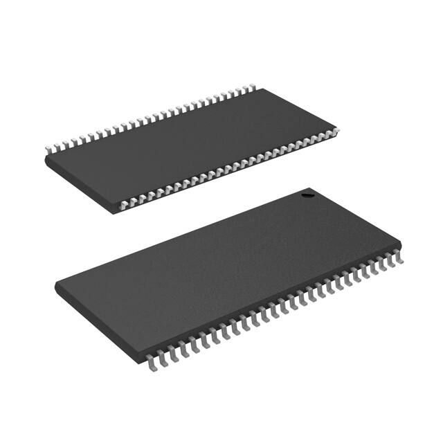
Available in Pb-free 54-pin TSOP II, and 48-ball VFBGA
packages
Functional Description
The CY7C1069G and CY7C1069GE are dual chip enable
high-performance CMOS fast static RAM devices with
embedded ECC. The CY7C1069G device is available in
standard pin configurations. The CY7C1069GE device includes
a single bit error indication pin (ERR) that signals the host
To write to the device, take Chip Enables (CE1 LOW and CE2
HIGH) and Write Enable (WE) input LOW. Data on the eight I/O
pins (I/O0 through I/O7) is then written into the location specified
on the address pins (A0 through A20).
To read from the device, take Chip Enables (CE1 LOW and CE2
HIGH) and Output Enable (OE) LOW while forcing the Write
Enable (WE) HIGH. Under these conditions, the contents of the
memory location specified by the address pins will appear on the
I/O pins. See Truth Table – CY7C1069G/CY7C1069GE on page
14 for a complete description of Read and Write modes. The
input and output pins (I/O0 through I/O7) are placed in a high
impedance state when the device is deselected (CE1 HIGH or
CE2 LOW), the outputs are disabled (OE HIGH), or during a write
operation (CE1 LOW, CE2 HIGH, and WE LOW).
On CY7C1069GE devices, the detection and correction of a
single-bit error in the accessed location is indicated by the
assertion of the ERR output (ERR = High) [1].
All I/Os (I/O0 through I/O7) are placed in a high impedance state
when the device is deselected (CE1 HIGH or CE2 LOW), and
control signals are de-asserted (CE1 / CE2, OE, WE).
CY7C1069G and CY7C1069GE devices are available in a
54-pin TSOP II package with center power and ground
(revolutionary) pinout, and in a 48-ball VFBGA package.
For a complete list of related documentation, here.
Note
1. Automatic write back on error detection feature is not supported in this device.
Cypress Semiconductor Corporation
Document Number: 001-81539 Rev. *J
•
198 Champion Court
•
San Jose, CA 95134-1709
•
408-943-2600
Revised December 5, 2017
�CY7C1069G
CY7C1069GE
Logic Block Diagram – CY7C1069G
2M x 8
RAM ARRAY
SENSE
AMPLIFIERS
ROW DECODER
A0
A1
A2
A3
A4
A5
A6
A7
A8
A9
ECC DECODER
DATAIN
DRIVERS
ECC ENCODER
I/O0‐I/O7
COLUMN
DECODER
A10
A11
A12
A13
A14
A15
A16
A17
A18
A19
A20
WE
OE
CE2
CE1
Logic Block Diagram – CY7C1069GE
2M x 8
RAM ARRAY
SENSE
AMPLIFIERS
ROW DECODER
A0
A1
A2
A3
A4
A5
A6
A7
A8
A9
I/O0‐I/O7
ERR
WE
OE
CE2
CE1
A10
A11
A12
A13
A14
A15
A16
A17
A18
A19
A20
COLUMN
DECODER
ECC DECODER
DATAIN
DRIVERS
ECC ENCODER
Document Number: 001-81539 Rev. *J
Page 2 of 20
�CY7C1069G
CY7C1069GE
Contents
Pin Configurations ........................................................... 4
Product Portfolio .............................................................. 6
Maximum Ratings ............................................................. 7
Operating Range ............................................................... 7
DC Electrical Characteristics .......................................... 7
Capacitance ...................................................................... 8
Thermal Resistance .......................................................... 8
AC Test Loads and Waveforms ....................................... 8
Data Retention Characteristics ....................................... 9
Data Retention Waveform ................................................ 9
AC Switching Characteristics ....................................... 10
Switching Waveforms .................................................... 11
Truth Table – CY7C1069G/CY7C1069GE ...................... 14
ERR Output – CY7C1069GE .......................................... 14
Document Number: 001-81539 Rev. *J
Ordering Information ...................................................... 15
Ordering Code Definitions ......................................... 15
Package Diagrams .......................................................... 16
Acronyms ........................................................................ 18
Document Conventions ................................................. 18
Units of Measure ....................................................... 18
Document History Page ................................................. 19
Sales, Solutions, and Legal Information ...................... 20
Worldwide Sales and Design Support ....................... 20
Products .................................................................... 20
PSoC®Solutions ....................................................... 20
Cypress Developer Community ................................. 20
Technical Support ..................................................... 20
Page 3 of 20
�CY7C1069G
CY7C1069GE
Pin Configurations
Figure 1. 54-pin TSOP II pinout (Top View) – CY7C1069G [2]
NC
VCC
NC
I/O6
VSS
I/O7
A4
A3
A2
A1
A0
NC
CE1
VCC
WE
CE2
A19
A18
A17
A16
A15
I/O0
VCC
I/O1
NC
VSS
NC
1
2
3
4
5
6
7
8
9
10
11
12
13
14
15
16
17
18
19
20
21
22
23
24
25
26
27
45
44
NC
VSS
NC
I/O5
VCC
I/O4
A5
A6
A7
A8
A9
43
42
41
40
39
38
37
36
35
34
33
32
31
30
29
28
NC
OE
VSS
NC
A20
A10
A11
A12
A13
A14
I/O3
VSS
I/O2
NC
VCC
NC
54
53
52
51
50
49
48
47
46
Figure 2. 54-pin TSOP II pinout (Top View) – CY7C1069GE [2, 3]
Note
2. NC pins are not connected on the die.
3. ERR is an Output pin. If not used, this pin should be left floating.
Document Number: 001-81539 Rev. *J
Page 4 of 20
�CY7C1069G
CY7C1069GE
Pin Configurations (continued)
Figure 3. 48-ball VFBGA pinout (Top View) – CY7C1069G [4]
1
2
3
4
5
6
NC
OE
A0
A1
A2
CE2
A
NC
NC
A3
A4
CE1
NC
B
I/O0
NC
A5
A6
NC
I/O4
C
VSS
I/O1
A17
A7
I/O5
VCC
D
VCC
I/O2
A18
A16
I/O6
VSS
E
I/O3
NC
A14
A15
NC
I/O7
F
NC
NC
A12
A13
WE
NC
G
A19
A8
A9
A10
A11
A20
H
Figure 4. 48-ball VFBGA pinout (Top View) – CY7C1069GE [4, 5]
Note
4. NC pins are not connected on the die.
5. ERR is an Output pin. If not used, this pin should be left floating.
Document Number: 001-81539 Rev. *J
Page 5 of 20
�CY7C1069G
CY7C1069GE
Product Portfolio
Power Dissipation
Product
Features and Options
(see the Pin
Configurations section)
Range
VCC Range (V) Speed
(ns)
Operating ICC, (mA)
f = fmax
Typ [6]
CY7C1069G18
Dual-chip enable
Industrial
Standby, ISB2 (mA)
Max
Typ [6]
Max
20
30
1.65 V–2.2 V
15
70
80
CY7C1069G30
2.2 V–3.6 V
10
90
110
CY7C1069G
4.5 V–5.5 V
10
90
110
CY7C1069GE18 Dual-chip enable and ERR
output
CY7C1069GE30
1.65 V–2.2 V
15
70
80
2.2 V–3.6 V
10
90
110
CY7C1069GE
4.5 V–5.5 V
10
90
110
Notes
6. Typical values are included for reference only and are not guaranteed or tested. Typical values are measured at VCC = 1.8 V (for VCC range of 1.65 V–2.2 V), VCC = 3 V
(for VCC range of 2.2 V–3.6 V), and VCC = 5 V (for VCC range of 4.5 V–5.5 V), TA = 25 °C.
Document Number: 001-81539 Rev. *J
Page 6 of 20
�CY7C1069G
CY7C1069GE
DC input voltage [7] ............................. –0.5 V to VCC + 0.5 V
Maximum Ratings
Exceeding maximum ratings may impair the useful life of the
device. These user guidelines are not tested.
Storage temperature ................................ –65 C to +150 C
Ambient temperature
with power applied ................................... –55 C to +125 C
Current into outputs (LOW) ........................................ 20 mA
Static Discharge Voltage
(MIL-STD-883, Method 3015) ................................. > 2001 V
Latch up current ..................................................... > 140 mA
Operating Range
Supply voltage
on VCC relative to GND ...............................–0.5 V to +6.0 V
DC voltage applied to outputs
in High Z State [7] ................................ –0.5 V to VCC + 0.5 V
Grade
Ambient Temperature
VCC
Industrial
–40 C to +85 C
1.65 V to 2.2 V,
2.2 V to 3.6 V,
4.5 V to 5.5 V
DC Electrical Characteristics
Over the Operating Range of –40 C to 85 C
Parameter
VOH
Description
Output HIGH
voltage
VIH
VIL
Output LOW
voltage
Input HIGH
voltage
Input LOW
voltage [7]
10 ns / 15 ns
Min
Typ [8]
Max
1.65 V to 2.2 V VCC = Min, IOH = –0.1 mA
2.2 V to 2.7 V VCC = Min, IOH = –1.0 mA
1.4
–
–
2.0
–
–
2.7 V to 3.0 V
VCC = Min, IOH = –4.0 mA
2.2
–
–
3.0 V to 3.6 V
VCC = Min, IOH = –4.0 mA
2.4
–
–
4.5 V to 5.5 V
VCC = Min, IOH = –4.0 mA
2.4
–
–
4.5 V to 5.5 V
VOL
Test Conditions
VCC = Min, IOH = –0.1 mA
VCC – 0.4
[9]
Unit
V
–
–
1.65 V to 2.2 V VCC = Min, IOL = 0.1 mA
2.2 V to 2.7 V VCC = Min, IOL = 2 mA
–
–
0.2
–
–
0.4
2.7 V to 3.6 V
VCC = Min, IOL = 8 mA
–
–
0.4
4.5 V to 5.5 V
VCC = Min, IOL = 8 mA
–
–
0.4
1.65 V to 2.2 V –
1.4
–
VCC + 0.2
2.2 V to 2.7 V
–
2.0
–
VCC + 0.3
2.7 V to 3.6 V
–
2.0
–
VCC + 0.3
4.5 V to 5.5 V
–
2.0
–
VCC + 0.5
1.65 V to 2.2 V –
–0.2
–
0.4
2.2 V to 2.7 V
–
–0.3
–
0.6
2.7 V to 3.6 V
–
–0.3
–
0.8
4.5 V to 5.5 V
–
–0.5
–
0.8
V
V
V
IIX
Input leakage current
GND < VIN < VCC
–1.0
–
+1.0
A
IOZ
Output leakage current
GND < VOUT < VCC, Output disabled
–1.0
–
+1.0
A
ICC
Operating supply current
VCC = Max, IOUT = 0 mA, f = 100 MHz
CMOS levels
f = 66.7 MHz
–
90.0
110.0
mA
–
70.0
80.0
ISB1
Automatic CE power down
current – TTL inputs
Max VCC, CE > VIH [10],
VIN > VIH or VIN < VIL, f = fMAX
–
–
40.0
mA
ISB2
Automatic CE power down
current – CMOS inputs
Max VCC, CE > VCC – 0.2 V [10],
VIN > VCC – 0.2 V or VIN < 0.2 V, f = 0
–
20.0 [8]
30.0
mA
Notes
7. VIL(min) = –2.0 V and VIH(max) = VCC + 2 V for pulse durations of less than 20 ns.
8. Typical values are included for reference only and are not guaranteed or tested. Typical values are measured at VCC = 1.8 V (for VCC range of 1.65 V–2.2 V), VCC = 3 V
(for VCC range of 2.2 V–3.6 V), and VCC = 5 V (for VCC range of 4.5 V–5.5 V), TA = 25 °C.
9. This parameter is guaranteed by design and is not tested.
10. For all dual chip enable devices, CE is the logical combination of CE1 and CE2. When CE1 is LOW and CE2 is HIGH, CE is LOW; when CE1 is HIGH or CE2 is LOW,
CE is HIGH.
Document Number: 001-81539 Rev. *J
Page 7 of 20
�CY7C1069G
CY7C1069GE
Capacitance
Parameter [11]
Description
CIN
Input capacitance
COUT
I/O capacitance
Test Conditions
54-pin TSOP II 48-ball VFBGA Unit
TA = 25 C, f = 1 MHz, VCC = VCC(typ)
10
10
pF
10
10
pF
Thermal Resistance
Parameter [11]
Description
JA
Thermal resistance
(junction to ambient)
JC
Thermal resistance
(junction to case)
Test Conditions
54-pin TSOP II 48-ball VFBGA Unit
Still air, soldered on a 3 × 4.5 inch,
four-layer printed circuit board
93.63
31.50
C/W
21.58
15.75
C/W
AC Test Loads and Waveforms
Figure 5. AC Test Loads and Waveforms [12]
High-Z Characteristics:
VCC
50
Output
VTH
Z0 = 50
Output
30 pF*
* Including
JIG and
Scope
(b)
All Input Pulses
VHIGH
GND
R2
5 pF*
(a)
* Capacitive load consists
of all components of the
test environment
R1
90%
90%
10%
Rise Time:
> 1 V/ns
10%
Fall Time:
> 1 V/ns
(c)
Parameters
1.8 V
3.0 V
5.0 V
Unit
R1
1667
317
317
R2
1538
351
351
VTH
0.9
1.5
1.5
V
VHIGH
1.8
3
3
V
Notes
11. Tested initially and after any design or process changes that may affect these parameters.
12. Full device AC operation assumes a 100-µs ramp time from 0 to VCC(min) and 100-µs wait time after VCC stabilization.
Document Number: 001-81539 Rev. *J
Page 8 of 20
�CY7C1069G
CY7C1069GE
Data Retention Characteristics
Over the Operating Range of –40 C to 85 C
Parameter
VDR
Description
Conditions
VCC for data retention
–
[13]
Min
Max
Unit
1.0
–
V
ICCDR
Data retention current
VCC = VDR, CE > VCC – 0.2 V
,
VIN > VCC – 0.2 V or VIN < 0.2 V
–
30.0
mA
tCDR[14]
Chip deselect to data retention
time
–
0
–
ns
tR[14, 15]
Operation recovery time
VCC > 2.2 V
10.0
–
ns
VCC < 2.2 V
15.0
–
ns
Data Retention Waveform
Figure 6. Data Retention Waveform [13]
VCC
VCC(min)
tCDR
DATA RETENTION MODE
VDR = 1.0 V
VCC(min)
tR
CE
Notes
13. For all dual chip enable devices, CE is the logical combination of CE1 and CE2. When CE1 is LOW and CE2 is HIGH, CE is LOW; when CE1 is HIGH or CE2 is LOW,
CE is HIGH.
14. This parameter is guaranteed by design and is not tested.
15. Full device operation requires linear VCC ramp from VDR to VCC(min.) > 100 s or stable at VCC(min.) > 100 s.
Document Number: 001-81539 Rev. *J
Page 9 of 20
�CY7C1069G
CY7C1069GE
AC Switching Characteristics
Over the Operating Range of –40 C to 85 C
Parameter [16]
Description
10 ns
15 ns
Min
Max
Min
Max
Unit
Read Cycle
tPOWER
VCC stable to first access [17, 18]
100.0
–
100.0
–
s
tRC
Read cycle time
10.0
–
15.0
–
ns
tAA
Address to data / ERR valid
–
10.0
–
15.0
ns
tOHA
Data / ERR hold from address change
3.0
–
3.0
–
ns
tACE
CE LOW to data / ERR valid [19]
–
10.0
–
15.0
ns
tDOE
OE LOW to data / ERR valid
–
5.0
–
8.0
ns
0
–
1.0
–
ns
tLZOE
OE LOW to low Z
[20, 21, 22]
[20, 21, 22]
tHZOE
OE HIGH to high Z
tLZCE
CE LOW to low Z [19, 20, 21, 22]
tHZCE
tPU
tPD
CE HIGH to high Z
–
5.0
–
8.0
ns
3.0
–
3.0
–
ns
[19, 20, 21, 22]
–
5.0
–
8.0
ns
[18, 19]
0
–
0
–
ns
–
10.0
–
15.0
ns
10.0
–
15.0
–
ns
7.0
–
12.0
–
ns
CE LOW to power-up
CE HIGH to power-down
[18, 19]
Write Cycle [23, 24]
tWC
Write cycle time
[19]
tSCE
CE LOW to write end
tAW
Address setup to write end
7.0
–
12.0
–
ns
tHA
Address hold from write end
0
–
0
–
ns
tSA
Address setup to write start
0
–
0
–
ns
tPWE
WE pulse width
7.0
–
12.0
–
ns
tSD
Data setup to write end
5.0
–
8.0
–
ns
tHD
Data hold from write end
0
–
0
–
ns
WE HIGH to low Z
[20, 21, 22]
3.0
–
3.0
–
ns
WE LOW to high Z
[20, 21, 22]
–
5.0
–
8.0
ns
tLZWE
tHZWE
Notes
16. Test conditions assume signal transition time (rise/fall) of 3 ns or less, timing reference levels of 1.5 V (for VCC > 3 V) and VCC/2 (for VCC < 3 V), and input pulse levels
of 0 to 3 V (for VCC > 3 V) and 0 to VCC (for VCC < 3V). Test conditions for the read cycle use output loading shown in part (a) of Figure 5 on page 8, unless specified otherwise.
17. tPOWER gives minimum amount of time that the power supply is at stable VCC until first memory access is performed.
18. These parameters are guaranteed by design and are not tested.
19. For all dual chip enable devices, CE is the logical combination of CE1 and CE2. When CE1 is LOW and CE2 is HIGH, CE is LOW; when CE1 is HIGH or CE2 is LOW,
CE is HIGH.
20. tHZOE, tHZCE, tHZWE, tLZOE, tLZCE, and tLZWE are specified with a load capacitance of 5 pF as in (b) of Figure 5 on page 8. Transition is measured 200 mV from steady state voltage.
21. At any temperature and voltage condition, tHZCE is less than tLZCE, tHZBE is less than tLZBE, tHZOE is less than tLZOE, and tHZWE is less than tLZWE for any device.
22. Tested initially and after any design or process changes that may affect these parameters.
23. The internal write time of the memory is defined by the overlap of WE = VIL, CE = VIL. These signals must be LOW to initiate a write, and the HIGH transition of any
of these signals can terminate the operation. The input data setup and hold timing should be referenced to the edge of the signal that terminates the write.
24. The minimum write pulse width for write cycle No.2 (WE Controlled, OE LOW) should be sum of tHZWE and tSD.
Document Number: 001-81539 Rev. *J
Page 10 of 20
�CY7C1069G
CY7C1069GE
Switching Waveforms
Figure 7. Read Cycle No. 1 of CY7C1069G (Address Transition Controlled) [25, 26]
tRC
ADDRESS
tAA
tOHA
DATA I/O
PREVIOUS DATAOUT
VALID
DATAOUT VALID
Figure 8. Read Cycle No. 2 of CY7C1069GE (Address Transition Controlled) [25, 26]
tRC
ADDRESS
tAA
tOHA
DATA I/O
PREVIOUS DATAOUT
VALID
DATAOUT VALID
tAA
tOHA
ERR
PREVIOUS ERR VALID
ERR VALID
Notes
25. The device is continuously selected, OE = VIL, CE = VIL.
26. WE is HIGH for read cycle.
Document Number: 001-81539 Rev. *J
Page 11 of 20
�CY7C1069G
CY7C1069GE
Switching Waveforms (continued)
Figure 9. Read Cycle No. 3 (OE Controlled, WE HIGH) [27, 28, 29]
ADDRESS
tRC
CE
tPD
t HZCE
tACE
OE
t HZOE
tDOE
t LZOE
DATA I/O
HIGH IMPEDANCE
DATAOUT VALID
HIGH
IMPEDANCE
t LZCE
VCC
SUPPLY
CURRENT
tPU
ISB
Notes
27. For all dual chip enable devices, CE is the logical combination of CE1 and CE2. When CE1 is LOW and CE2 is HIGH, CE is LOW; when CE1 is HIGH or CE2 is LOW,
CE is HIGH.
28. WE is HIGH for read cycle.
29. Address valid prior to or coincident with CE LOW transition.
Document Number: 001-81539 Rev. *J
Page 12 of 20
�CY7C1069G
CY7C1069GE
Switching Waveforms (continued)
Figure 10. Write Cycle No. 1 (CE Controlled) [30, 31, 32]
tWC
ADDRESS
tSA
tSCE
CE
tAW
tHA
t PWE
WE
OE
t HZOE
DATA I/O
tHD
tSD
DATAIN VALID
Note 33
Figure 11. Write Cycle No. 2 (WE Controlled, OE Low) [30, 31, 32, 34]
tWC
ADDRESS
tSCE
CE
tSA
tAW
tHA
t PWE
WE
t HZWE
DATA I/O
Note 33
tSD
t LZWE
tHD
DATAIN VALID
Notes
30. For all dual chip enable devices, CE is the logical combination of CE1 and CE2. When CE1 is LOW and CE2 is HIGH, CE is LOW; when CE1 is HIGH or CE2 is LOW,
CE is HIGH.
31. The internal write time of the memory is defined by the overlap of WE = VIL, CE = VIL. These signals must be LOW to initiate a write, and the HIGH transition of any
of these signals can terminate the operation. The input data setup and hold timing should be referenced to the edge of the signal that terminates the write.
32. Data I/O is in high impedance state if CE = VIH, or OE = VIH.
33. During this time I/O are in output put state. Do not apply input signals.
34. The minimum write cycle width should be sum of tHZWE and tSD,
Document Number: 001-81539 Rev. *J
Page 13 of 20
�CY7C1069G
CY7C1069GE
Truth Table – CY7C1069G/CY7C1069GE
CE1
H
X
CE2
X
[35]
OE
X
[35]
X
[35]
WE
I/O0–I/O7
Mode
Power
X
[35]
High Z
Power-down
Standby (ISB)
X
[35]
High Z
Power-down
Standby (ISB)
[35]
L
L
H
L
H
Data out
Read all bits
Active (ICC)
L
H
[35]
L
Data in
Write all bits
Active (ICC)
L
H
H
H
High Z
Selected, outputs disabled
Active (ICC)
X
ERR Output – CY7C1069GE
Output [36]
Mode
0
Read Operation, no single bit error in the stored data.
1
Read Operation, single bit error detected and corrected.
High Z
Device deselected or Outputs disabled or Write Operation
Note
35. The input voltage levels on these pins should be either at VIH or VIL.
36. ERR is an Output pin.If not used, this pin should be left floating.
Document Number: 001-81539 Rev. *J
Page 14 of 20
�CY7C1069G
CY7C1069GE
Ordering Information
Speed
(ns)
10
Voltage
Range
Package
Diagram
Ordering Code
2.2 V–3.6 V CY7C1069G30-10BVXI
Package Type
(All Pb-free)
ERR Pin /
Ball
Operating
Range
Industrial
51-85150 48-ball VFBGA
No
CY7C1069G30-10BVXIT
51-85150 48-ball VFBGA, Tape and Reel
No
CY7C1069G30-10ZSXI
51-85160 54-pin TSOP II
No
CY7C1069G30-10ZSXIT
51-85160 54-pin TSOP II, Tape and Reel
No
CY7C1069GE30-10ZSXI
51-85160 54-pin TSOP II
Yes
CY7C1069GE30-10ZSXIT
51-85160 54-pin TSOP II, Tape and Reel
Yes
51-85150 48-ball VFBGA
No
CY7C1069G-10BVXIT
51-85150 48-ball VFBGA, Tape and Reel
No
CY7C1069G-10ZSXI
51-85160 54-pin TSOP II
No
CY7C1069G-10ZSXIT
51-85160 54-pin TSOP II, Tape and Reel
No
4.5 V–5.5 V CY7C1069G-10BVXI
Ordering Code Definitions
CY 7 C 1 06 9
G
E
XX - XX XX X
I
X
X = blank or T
blank = Bulk; T = Tape and Reel
Temperature Range:
I = Industrial
Pb-free
Package Type: XX = BV or ZS
BV = 48-ball VFBGA; ZS = 54-pin TSOP II
Speed: XX = 10 ns or 15 ns
Voltage Range:
18 = 1.65 V–2.2 V; 30 = 2.2 V–3.6 V; no character = 4.5 V–5.5 V
X = blank or E
blank = without ERR output;
E = with ERR output, single bit error indication
Process Technology: G = ULL65, 65 nm
Data Width: 9 = × 8-bits
Density: 06 = 16-Mbit
Family Code: 1 = Fast Asynchronous SRAM family
Technology Code: C = CMOS
Marketing Code: 7 = SRAM
Company ID: CY = Cypress
Document Number: 001-81539 Rev. *J
Page 15 of 20
�CY7C1069G
CY7C1069GE
Package Diagrams
Figure 12. 54-pin TSOP II (22.4 × 11.84 × 1.0 mm) Z54-II Package Outline, 51-85160
51-85160 *E
Document Number: 001-81539 Rev. *J
Page 16 of 20
�CY7C1069G
CY7C1069GE
Package Diagrams (continued)
Figure 13. 48-ball VFBGA (6 × 8 × 1.0 mm) BV48/BZ48 Package Outline, 51-85150
51-85150 *H
Document Number: 001-81539 Rev. *J
Page 17 of 20
�CY7C1069G
CY7C1069GE
Acronyms
Acronym
Document Conventions
Description
Units of Measure
CE
Chip Enable
CMOS
Complementary Metal Oxide Semiconductor
°C
degree Celsius
I/O
Input/Output
MHz
megahertz
OE
Output Enable
A
microampere
SRAM
Static Random Access Memory
s
microsecond
TSOP
Thin Small Outline Package
mA
milliampere
TTL
Transistor-Transistor Logic
mm
millimeter
VFBGA
Very Fine-Pitch Ball Grid Array
ns
nanosecond
WE
Write Enable
ohm
%
percent
pF
picofarad
V
volt
W
watt
Document Number: 001-81539 Rev. *J
Symbol
Unit of Measure
Page 18 of 20
�CY7C1069G
CY7C1069GE
Document History Page
Document Title: CY7C1069G/CY7C1069GE, 16-Mbit (2M words × 8 bit) Static RAM with Error-Correcting Code (ECC)
Document Number: 001-81539
Rev.
ECN No.
Orig. of
Change
Submission
Date
*H
4800609
NILE
07/31/2015
Changed status from Preliminary to Final.
*I
5436514
NILE
09/14/2016
Updated Maximum Ratings:
Updated Note 7 (Replaced “2 ns” with “20 ns”).
Updated DC Electrical Characteristics:
Removed Operating Range “2.7 V to 3.6 V” and all values corresponding to
VOH parameter.
Included Operating Ranges “2.7 V to 3.0 V” and “3.0 V to 3.6 V” and all values
corresponding to VOH parameter.
Changed minimum value of VIH parameter from 2.2 V to 2 V corresponding
to Operating Range “4.5 V to 5.5 V”.
Updated Ordering Information:
Updated part numbers.
Updated to new template.
*J
5984763
AESATMP9
12/05/2017
Updated logo and copyright.
Document Number: 001-81539 Rev. *J
Description of Change
Page 19 of 20
�CY7C1069G
CY7C1069GE
Sales, Solutions, and Legal Information
Worldwide Sales and Design Support
Cypress maintains a worldwide network of offices, solution centers, manufacturer’s representatives, and distributors. To find the office
closest to you, visit us at Cypress Locations.
PSoC®Solutions
Products
ARM® Cortex® Microcontrollers
Automotive
cypress.com/arm
cypress.com/automotive
Clocks & Buffers
Interface
cypress.com/clocks
cypress.com/interface
Internet of Things
Memory
cypress.com/iot
cypress.com/memory
Microcontrollers
cypress.com/mcu
PSoC
cypress.com/psoc
Power Management ICs
Touch Sensing
USB Controllers
Wireless Connectivity
PSoC 1 | PSoC 3 | PSoC 4 | PSoC 5LP | PSoC 6
Cypress Developer Community
Forums | WICED IOT Forums | Projects | Video | Blogs |
Training | Components
Technical Support
cypress.com/support
cypress.com/pmic
cypress.com/touch
cypress.com/usb
cypress.com/wireless
© Cypress Semiconductor Corporation, 2012-2017. This document is the property of Cypress Semiconductor Corporation and its subsidiaries, including Spansion LLC ("Cypress"). This document,
including any software or firmware included or referenced in this document ("Software"), is owned by Cypress under the intellectual property laws and treaties of the United States and other countries
worldwide. Cypress reserves all rights under such laws and treaties and does not, except as specifically stated in this paragraph, grant any license under its patents, copyrights, trademarks, or other
intellectual property rights. If the Software is not accompanied by a license agreement and you do not otherwise have a written agreement with Cypress governing the use of the Software, then Cypress
hereby grants you a personal, non-exclusive, nontransferable license (without the right to sublicense) (1) under its copyright rights in the Software (a) for Software provided in source code form, to
modify and reproduce the Software solely for use with Cypress hardware products, only internally within your organization, and (b) to distribute the Software in binary code form externally to end users
(either directly or indirectly through resellers and distributors), solely for use on Cypress hardware product units, and (2) under those claims of Cypress's patents that are infringed by the Software (as
provided by Cypress, unmodified) to make, use, distribute, and import the Software solely for use with Cypress hardware products. Any other use, reproduction, modification, translation, or compilation
of the Software is prohibited.
TO THE EXTENT PERMITTED BY APPLICABLE LAW, CYPRESS MAKES NO WARRANTY OF ANY KIND, EXPRESS OR IMPLIED, WITH REGARD TO THIS DOCUMENT OR ANY SOFTWARE
OR ACCOMPANYING HARDWARE, INCLUDING, BUT NOT LIMITED TO, THE IMPLIED WARRANTIES OF MERCHANTABILITY AND FITNESS FOR A PARTICULAR PURPOSE. To the extent
permitted by applicable law, Cypress reserves the right to make changes to this document without further notice. Cypress does not assume any liability arising out of the application or use of any
product or circuit described in this document. Any information provided in this document, including any sample design information or programming code, is provided only for reference purposes. It is
the responsibility of the user of this document to properly design, program, and test the functionality and safety of any application made of this information and any resulting product. Cypress products
are not designed, intended, or authorized for use as critical components in systems designed or intended for the operation of weapons, weapons systems, nuclear installations, life-support devices or
systems, other medical devices or systems (including resuscitation equipment and surgical implants), pollution control or hazardous substances management, or other uses where the failure of the
device or system could cause personal injury, death, or property damage ("Unintended Uses"). A critical component is any component of a device or system whose failure to perform can be reasonably
expected to cause the failure of the device or system, or to affect its safety or effectiveness. Cypress is not liable, in whole or in part, and you shall and hereby do release Cypress from any claim,
damage, or other liability arising from or related to all Unintended Uses of Cypress products. You shall indemnify and hold Cypress harmless from and against all claims, costs, damages, and other
liabilities, including claims for personal injury or death, arising from or related to any Unintended Uses of Cypress products.
Cypress, the Cypress logo, Spansion, the Spansion logo, and combinations thereof, WICED, PSoC, CapSense, EZ-USB, F-RAM, and Traveo are trademarks or registered trademarks of Cypress in
the United States and other countries. For a more complete list of Cypress trademarks, visit cypress.com. Other names and brands may be claimed as property of their respective owners.
Document Number: 001-81539 Rev. *J
Revised December 5, 2017
Page 20 of 20
�


 工商网监
湘ICP备2023018690号
工商网监
湘ICP备2023018690号
