CY7C135, CY7C135A
CY7C1342
4K x 8 Dual-Port Static RAM and 4K x 8
Dual-Port SRAM with Semaphores
Features
Functional Description
■
True dual-ported memory cells, which allow simultaneous
reads of the same memory location
■
4K x 8 organization
■
0.65 micron CMOS for optimum speed and power
■
High speed access: 15 ns
■
Low operating power: ICC = 160 mA (max)
The CY7C135/135A[1] and CY7C1342 are high speed CMOS 4K
x 8 dual-port static RAMs. The CY7C1342 includes semaphores
that provide a means to allocate portions of the dual-port RAM
or any shared resource. Two ports are provided permitting
independent, asynchronous access for reads and writes to any
location in memory. Application areas include interprocessor/multiprocessor
designs,
communications
status
buffering, and dual-port video/graphics memory.
■
Fully asynchronous operation
■
Automatic power down
■
Semaphores included on the 7C1342 to permit software
handshaking between ports
■
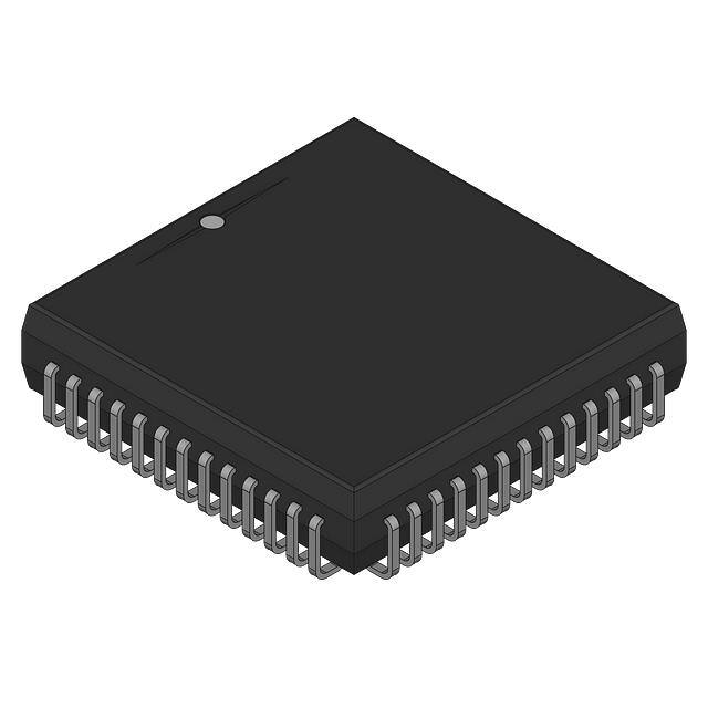
Available in 52-pin PLCC
■
Pb-free packages available
Each port has independent control pins: chip enable (CE), read
or write enable (R/W), and output enable (OE). The
CY7C135/135A is suited for those systems that do not require
on-chip arbitration or are intolerant of wait states. Therefore, the
user must be aware that simultaneous access to a location is
possible. Semaphores are offered on the CY7C1342 to assist in
arbitrating between ports. The semaphore logic is comprised of
eight shared latches. Only one side can control the latch
(semaphore) at any time. Control of a semaphore indicates that
a shared resource is in use. An automatic power down feature is
controlled independently on each port by a chip enable (CE) pin
or SEM pin (CY7C1342 only).
The CY7C135/135A and CY7C1342 are available in 52-pin
PLCC.
Logic Block Diagram
R/WL
R/WR
CEL
OEL
CER
OER
I/O7L
I/O
CONTROL
I/O0L
I/O7R
I/O
CONTROL
I/O0R
A11L
A11R
ADDRESS
DECODER
A0L
CEL
MEMORY
ARRAY
SEMAPHORE
ARBITRATION
(7C1342 only)
OEL
ADDRESS
DECODER
A0R
CER
OER
R/WL
R/WR
(7C1342 only)
(7C1342 only) SEML
SEMR
Note
1. CY7C135 and CY7C135A are functionally identical
Cypress Semiconductor Corporation
Document #: 38-06038 Rev. *D
•
198 Champion Court
•
San Jose, CA 95134-1709
•
408-943-2600
Revised December 09, 2008
[+] Feedback
�CY7C135, CY7C135A
CY7C1342
Selection Guide
Parameter
Maximum Access Time
7C135-15
7C1342-15
15
7C135-20
7C1342-20
20
7C135/135A-25
7C1342-25
25
7C135-35
7C1342-35
35
7C135-55
7C1342-55
55
Unit
220
60
190
50
180
40
160
30
160
30
mA
mA
Maximum Operating Current Commercial
Maximum Standby Current for Commercial
ISB1
ns
Pin Configurations
7 6 5 4 3 2 1 52 51 50 49 48 47
46
45
44
43
42
41
7C1342
40
39
38
37
36
35
34
21 22 23 24 25 26 27 28 29 30 31 32 33
OER
A0R
A1R
A2R
A3R
A4R
A5R
A6R
A7R
A8R
A9R
NC
I/O7R
NC
GND
I/O0R
I/O1R
I/O2R
I/O3R
I/O4R
I/O5R
I/O6R
8
9
10
11
12
13
14
15
16
17
18
19
20
CER
R/WR
SEMR
A11R
A10R
A0L
OEL
A10L
A11L
A6R
A7R
A8R
A9R
NC
I/O7R
A1L
A2L
A3L
A4L
A5L
A6L
A7L
A8L
A9L
I/O0L
I/O1L
I/O2L
I/O3L
I/O 4L
I/O 5L
I/O 6L
I/O 7L
OER
A0R
A1R
A2R
A3R
A4R
A5R
SEM L
R/W
L
CEL
VCC
Figure 2. Pin Diagram - CY7C1342 (Top View)
CER
R/WR
N/C
A11R
A10R
7 6 5 4 3 2 1 52 51 50 49 48 47
46
45
44
43
42
41
7C135/135A
40
39
38
37
36
35
34
21 22 23 24 25 26 27 28 29 30 31 32 33
NC
GND
I/O0R
I/O1R
I/O2R
I/O3R
I/O4R
I/O5R
I/O6R
8
9
10
11
12
13
14
15
16
17
18
19
20
I/O4L
I/O5L
I/O6L
I/O7L
A1L
A2L
A3L
A4L
A5L
A6L
A7L
A8L
A9L
I/O0L
I/O1L
I/O2L
I/O3L
A11L
N/C
R/W
L
CEL
VCC
A0L
OEL
A10L
Figure 1. Pin Diagram - CY7C135/135A (Top View)
Pin Definitions
Left Port
Right Port
Description
A0L–11L
A0R–11R
Address Lines
CEL
CER
Chip Enable
OEL
OER
Output Enable
R/WL
R/WR
Read/Write Enable
SEML
(CY7C1342
only)
SEMR
(CY7C1342
only)
Semaphore Enable. When asserted LOW, allows access to eight semaphores. The three least
significant bits of the address lines determines which semaphore to write or read. The I/O0 pin
is used when writing to a semaphore. Semaphores are requested by writing a 0 into the
respective location.
Document #: 38-06038 Rev. *D
Page 2 of 12
[+] Feedback
�CY7C135, CY7C135A
CY7C1342
DC Input Voltage[3] .........................................–3.0V to +7.0V
Maximum Ratings[2]
Exceeding maximum ratings may shorten the useful life of the
device. User guidelines are not tested.
Storage Temperature .................................. –65°C to+150°C
Ambient Temperature with
Power Applied ............................................. –55°C to+125°C
Static Discharge Voltage........................................... > 2001V
(per MIL-STD-883, Method 3015)
Latch Up Current .................................................... > 200 mA
Operating Range
Supply Voltage to Ground Potential
(Pin 48 to Pin 24)............................................ –0.5V to+7.0V
Range
Ambient
Temperature
VCC
Commercial
0°C to +70°C
5V ± 10%
Industrial
–40°C to +85°C
5V ± 10%
DC Voltage Applied to Outputs
in High Z State ................................................ –0.5V to+7.0V
Electrical Characteristics Over the Operating Range
Parameter
Description
Test Conditions
7C135-15
7C1342-15
7C135-20
7C1342-20
7C135-25
7C135A-25
7C1342-25 Unit
Min
Min
Min
Max
2.4
Max
Output HIGH Voltage
VCC = Min., IOH = –4.0 mA
VOL
Output LOW Voltage
VCC = Min., IOL = 4.0 mA
VIH
Input HIGH Voltage
VIL
Input LOW Voltage
0.8
V
IIX
Input Load Current
GND ≤ VI ≤ VCC
–10
+10
–10
+10
–10
+10
μA
IOZ
Output Leakage Current
Outputs Disabled,
GND ≤ VO ≤ VCC
–10
+10
–10
+10
–10
+10
μA
ICC
Operating Current
VCC = Max.,
IOUT = 0 mA
Com’l
180
mA
0.4
2.2
2.2
CEL and CER ≥ VIH,
f = fMAX[4]
Com’l
ISB2
Standby Current
(One Port TTL Level)
CEL and CER ≥ VIH,
f = fMAX[4]
Com’l
190
Standby Current
(One Port CMOS Level)
Com’l
V
60
50
40
130
120
110
mA
50
mA
120
15
15
Ind.
Ind.
V
190
Ind.
Com’l
0.4
0.8
Ind.
Standby Current
Both Ports CE and CER ≥ VCC –
(Both Ports CMOS Levels) 0.2V,
VIN ≥ VCC – 0.2V
or VIN ≤ 0.2V, f = 0[4]
One Port CEL or
CER ≥ VCC – 0.2V,
VIN ≥VCC – 0.2V or
VIN ≤ 0.2V,
Active Port Outputs,
f = fMAX[4]
220
V
2.2
Ind.
Standby Current
(Both Ports TTL Levels)
ISB4
2.4
0.4
0.8
ISB1
ISB3
2.4
Max
VOH
15
mA
30
125
115
100
mA
115
Notes
2. The voltage on any input or I/O pin cannot exceed the power pin during power up.
3. Pulse width < 20 ns.
4. fMAX = 1/tRC = All inputs cycling at f = 1/tRC (except output enable). f = 0 means no address or control lines change. This applies only to inputs at CMOS level standby
ISB3.
Document #: 38-06038 Rev. *D
Page 3 of 12
[+] Feedback
�CY7C135, CY7C135A
CY7C1342
Electrical Characteristics Over the Operating Range (continued)
Parameter
Description
Test Conditions
VOH
Output HIGH Voltage
VCC = Min., IOH = –4.0 mA
VOL
Output LOW Voltage
VCC = Min., IOL = 4.0 mA
7C135-35
7C1342-35
7C135-55
7C1342-55
Min
Min
Max
2.4
2.4
0.4
2.2
VIH
Unit
Max
V
0.4
V
0.8
V
2.2
Input LOW Voltage
IIX
Input Load Current
GND ≤ VI ≤ VCC
–10
+10
–10
+10
μA
IOZ
Output Leakage Current
Outputs Disabled, GND ≤ VO ≤ VCC
–10
+10
–10
+10
μA
ICC
Operating Current
mA
ISB1
ISB2
0.8
V
VIL
VCC = Max., IOUT = 0 mA
Com’l
160
160
VCC = Max., IOUT = 0 mA
Ind.
180
180
Com’l
30
30
Ind.
40
40
Com’l
100
100
Ind.
110
110
Com’l
15
15
Ind.
30
30
Com’l
90
90
Ind.
100
100
Standby Current
(Both Ports TTL Levels)
CEL and CER ≥ VIH, f = fMAX[4]
Standby Current
(One Port TTL Level)
CEL and CER ≥ VIH, f = fMAX
[4]
Standby Current
Both Ports CE and CER ≥ VCC – 0.2V,
(Both Ports CMOS Levels) VIN ≥ VCC – 0.2V
or VIN ≤ 0.2V, f = 0[4]
ISB3
One Port CEL or CER ≥ VCC – 0.2V,
VIN ≥ VCC – 0.2V or VIN ≤ 0.2V,
Active Port Outputs, f = fMAX[4]
Standby Current
(One Port CMOS Level)
ISB4
mA
mA
mA
mA
Capacitance[5]
Parameter
Description
CIN
Input Capacitance
COUT
Output Capacitance
Test Conditions
TA = 25°C, f = 1 MHz,
VCC = 5.0V
Max.
Unit
10
pF
10
pF
Figure 3. AC Test Loads and Waveforms
5V
R1 = 893Ω
C = 30 pF
RTH = 250Ω
RTH = 250Ω
OUTPUT
OUTPUT
OUTPUT
C = 5 pF
C = 30 pF
R1 = 347Ω
VTH = 1.4V
(a) Normal Load (Load 1)
(b) Thévenin Equivalent (Load 1)
VX
(c) Three-State Delay (Load 3)
ALL INPUT PULSES
3.0V
GND
10%
90%
≤ 3 ns
90%
10%
≤ 3 ns
Note
5. Tested initially and after any design or process changes that may affect these parameters.
Document #: 38-06038 Rev. *D
Page 4 of 12
[+] Feedback
�CY7C135, CY7C135A
CY7C1342
Switching Characteristics Over the Operating Range[6]
Parameter
Description
7C135-15
7C1342-15
7C135-20
7C1342-20
7C135-25
7C135A-25
7C1342-25
7C135-35
7C1342-35
7C135-55
7C1342-55
Min
Min
Min
Min
Min
Max
Max
Max
Max
Unit
Max
Read Cycle
tRC
Read Cycle Time
tAA
Address to Data Valid
tOHA
Output Hold From Address Change
tACE
CE LOW to Data Valid
tDOE
OE LOW to Data Valid
tLZOE[7,8,9]
OE Low to Low Z
tHZOE[7,8,9]
OE HIGH to High Z
tLZCE[7,8,9]
tHZCE[7,8,9]
tPU[9]
tPD[9]
CE LOW to Low Z
15
3
3
3
3
3
10
0
13
25
3
20
15
25
20
25
ns
ns
ns
25
0
35
ns
ns
3
0
ns
ns
55
20
3
0
20
3
3
15
ns
55
35
15
3
0
15
3
3
13
55
35
25
13
3
10
35
25
20
10
3
CE HIGH to Power Down
25
20
15
CE HIGH to High Z
CE LOW to Power Up
20
15
ns
ns
55
ns
Write Cycle
tWC
Write Cycle Time
15
20
25
35
55
ns
tSCE
CE LOW to Write End
12
15
20
30
50
ns
tAW
Address Setup to Write End
12
15
20
30
50
ns
tHA
Address Hold from Write End
2
2
2
2
2
ns
tSA
Address Setup to Write Start
0
0
0
0
0
ns
tPWE
Write Pulse Width
12
15
20
25
50
ns
tSD
Data Setup to Write End
10
13
15
15
25
ns
Data Hold from Write End
0
0
0
0
0
ns
tHD
[8,9]
R/W LOW to High Z
tLZWE[8,9]
R/W HIGH to Low Z
tWDD[10]
tDDD[10]
Write Pulse to Data Delay
30
40
50
60
70
ns
Write Data Valid to Read Data Valid
25
30
30
35
40
ns
tHZWE
10
3
13
3
15
3
20
3
25
3
ns
ns
[11]
Semaphore Timing
tSOP
SEM Flag Update Pulse
(OE or SEM)
10
10
10
15
15
ns
tSWRD
SEM Flag Write to Read Time
5
5
5
5
5
ns
tSPS
SEM Flag Contention Window
5
5
5
5
5
ns
Notes
6. Test conditions assume signal transition time of 3 ns or less, timing reference levels of 1.5V, input pulse levels of 0 to 3.0V, and output loading of the specified IOL/IOH
and 30 pF load capacitance.
7. At any given temperature and voltage condition for any given device, tHZCE is less than tLZCE and tHZOE is less than tLZOE.
8. Test conditions used are Load 3.
9. This parameter is guaranteed but not tested.
10. For information on port-to-port delay through RAM cells from writing port to reading port, refer to Figure 6.
11. Semaphore timing applies only to CY7C1342.
Document #: 38-06038 Rev. *D
Page 5 of 12
[+] Feedback
�CY7C135, CY7C135A
CY7C1342
Switching Waveforms
Figure 4. Read Cycle No. 1[12,13]
Either Port Address Access
tRC
ADDRESS
tAA
tOHA
DATA OUT
PREVIOUS DATA VALID
DATA VALID
Figure 5. Read Cycle No. 2[12,14]
Either Port CE/OE Access
SEM
[11]
or CE
tHZCE
tACE
OE
tLZOE
tHZOE
tDOE
tLZCE
DATA VALID
DATA OUT
tPU
tPD
ICC
ISB
Figure 6. Read Timing with Port-to-Port[15]
twc
ADDRESSR
MATCH
t
R/WR
PWE
t
DATAINR
ADDRESSL
t
SD
HD
VALID
MATCH
tDDD
DATAOUTL
VALID
tWDD
Notes
12. R/W is HIGH for read cycle.
13. Device is continuously selected, CE = VIL and OE = VIL.
14. Address valid prior to or coincident with CE transition LOW.
15. CEL = CER =LOW; R/WL = HIGH
Document #: 38-06038 Rev. *D
Page 6 of 12
[+] Feedback
�CY7C135, CY7C135A
CY7C1342
Switching Waveforms (continued)
Figure 7. Write Cycle No. 1: OE Three-States Data I/Os (Either Port)[16, 17, 18]
tWC
ADDRESS
tSCE
[11]
SEM
OR CE
tAW
tHA
tPWE
R/W
tSA
tSD
DATAIN
tHD
DATA VALID
OE
t
tHZOE
LZOE
HIGH IMPEDANCE
DATAOUT
Figure 8. Write Cycle No. 2: R/W Three-States Data I/Os (Either Port)[17, 19]
tWC
ADDRESS
tHA
tSCE
[11]
SEM
OR CE
tSA
tAW
tPWE
R/W
tSD
DATA VALID
DATAIN
tHZWE
DATAOUT
tHD
tLZWE
HIGH IMPEDANCE
Notes
16. The internal write time of the memory is defined by the overlap of CE or SEM LOW and R/W LOW. Both signals must be LOW to initiate a write and either signal
can terminate a write by going HIGH. The data input setup and hold timing should be referenced to the rising edge of the signal that terminates the write.
17. R/W must be HIGH during all address transactions.
18. If OE is LOW during a R/W controlled write cycle, the write pulse width must be the larger of tPWE or (tHZWE + tSD) to allow the I/O drivers to turn off and data
to be placed on the bus for the required tSD. If OE is HIGH during a R/W controlled write cycle (as in this example), this requirement does not apply and the
write pulse can be as short as the specified tPWE.
19. Data I/O pins enter high impedance when OE is held LOW during write.
Document #: 38-06038 Rev. *D
Page 7 of 12
[+] Feedback
�CY7C135, CY7C135A
CY7C1342
Switching Waveforms (continued)
Figure 9. Semaphore Read After Write Timing, Either Side (CY7C1342 only)[20]
tAA
A0–A2
VALID ADDRESS
VALID ADDRESS
tAW
SEM
tACE
tHA
tSCE
tOHA
tSOP
tSD
I/O0
DATAINVALID
tSA
DATAOUT VALID
tHD
tPWE
R/W
tDOE
tSWRD
tSOP
OE
WRITE CYCLE
READ CYCLE
Figure 10. Timing Diagram of Semaphore Contention (CY7C1342 Only)[21, 22, 23]
A0L–A2L
MATCH
R/WL
SEML
tSPS
A0R–A2R
MATCH
R/WR
SEMR
Notes
20. CE = HIGH for the duration of the above timing (both write and read cycle).
21. I/O0R = I/O0L = LOW (request semaphore); CER = CEL = HIGH.
22. Semaphores are reset (available to both ports) at cycle start.
23. If tSPS is violated, it is guaranteed that only one side gains access to the semaphore.
Document #: 38-06038 Rev. *D
Page 8 of 12
[+] Feedback
�CY7C135, CY7C135A
CY7C1342
Architecture
The CY7C135/135A consists of an array of 4K words of 8 bits
each of dual-port RAM cells, I/O and address lines, and control
signals (CE, OE, R/W). Two semaphore control pins exist for the
CY7C1342 (SEML/R).
Functional Description
Write Operation
Data must be set up for a duration of tSD before the rising edge
of R/W to guarantee a valid write. Because there is no on-chip
arbitration, the user must be sure that a specific location is not
accessed simultaneously by both ports or erroneous data could
result. A write operation is controlled by either the OE pin (see
Figure 7) or the R/W pin (see Figure 8). Data can be written
tHZOE after the OE is deasserted or tHZWE after the falling edge
of R/W. Required inputs for write operations are summarized in
Table 1.
If a location is being written to by one port and the opposite port
attempts to read the same location, a port-to-port flowthrough
delay is met before the data is valid on the output. Data is valid
on the port wishing to read the location tDDD after the data is
presented on the writing port.
now only be modified by the side showing a zero (the left port in
this case). If the left port now relinquishes control by writing a one
to the semaphore, the semaphore is set to one for both sides.
However, if the right port had requested the semaphore (written
a zero) while the left port had control, the right port would immediately own the semaphore. Table 2 shows sample semaphore
operations.
When reading a semaphore, all eight data lines output the
semaphore value. The read value is latched in an output register
to prevent the semaphore from changing state during a write
from the other port. If both ports request a semaphore control by
writing a 0 to a semaphore within tSPS of each other, it is
guaranteed that only one side gains access to the semaphore.
Initialization of the semaphore is not automatic and must be reset
during initialization program during power up. All semaphores on
both sides should have a one written into them at initialization
from both sides to assure that they are free when needed.
Table 1. Non-Contending Read/Write
Inputs
Outputs
Operation
CE
R/W
OE
SEM
H
X
X
H
H
H
L
L
Data Out
Read Semaphore
Read Operation
X
X
H
X
High Z
I/O Lines Disabled
When reading the device, the user must assert both the OE and
CE pins. Data is available tACE after CE or tDOE after OE are
asserted. If the user of the CY7C1342 wishes to access a
semaphore, the SEM pin must be asserted instead of the CE pin.
Required inputs for read operations are summarized in Table 1.
H
L
X
L
Data In
Write to Semaphore
L
H
L
H
Data Out
Read
L
L
X
H
Data In
Write
L
X
X
L
Semaphore Operation
The CY7C1342 provides eight semaphore latches, which are
separate from the dual port memory locations. Semaphores are
used to reserve resources which are shared between the two
ports. The state of the semaphore indicates that a resource is in
use. For example, if the left port wants to request a given
resource, it sets a latch by writing a zero to a semaphore location.
The left port then verifies its success in setting the latch by
reading it. After writing to the semaphore, SEM or OE must be
deasserted for tSOP before attempting to read the semaphore.
The semaphore value is available tSWRD + tDOE after the rising
edge of the semaphore write. If the left port was successful
(reads a zero), it assumes control over the shared resource,
otherwise (reads a one) it assumes the right port has control and
continues to poll the semaphore. When the right side has relinquished control of the semaphore (by writing a one), the left side
succeeds in gaining control of the semaphore. If the left side no
longer requires the semaphore, a one is written to cancel its
request.
I/O0 – I/O7
High Z
Power Down
Illegal Condition
Table 2. Semaphore Operation Example
Function
I/O0-7 I/O0-7
Left Right
Status
No action
1
1
Semaphore free
Left port writes
semaphore
0
1
Left port obtains
semaphore
Right port writes 0 to
semaphore
0
1
Right side is denied
access
Left port writes 1 to
semaphore
1
0
Right port is granted
access to Semaphore
Left port writes 0 to
semaphore
1
0
No change. Left port is
denied access
Right port writes 1 to
semaphore
0
1
Left port obtains
semaphore
Left port writes 1 to
semaphore
1
1
No port accessing
semaphore address
Semaphores are accessed by asserting SEM LOW. The SEM
pin functions as a chip enable for the semaphore latches. CE
must remain HIGH during SEM LOW. A0–2 represents the
semaphore address. OE and R/W are used in the same manner
as a normal memory access. When writing or reading a
semaphore, the other address pins have no effect.
Right port writes 0 to
semaphore
1
0
Right port obtains
semaphore
Right port writes 1 to
semaphore
1
1
No port accessing
semaphore
Left port writes 0 to
semaphore
0
1
Left port obtains
semaphore
When writing to the semaphore, only I/O0 is used. If a 0 is written
to the left port of an unused semaphore, a one appears at the
same semaphore address on the right port. That semaphore can
Left port writes 1 to
semaphore
1
1
No port accessing
semaphore
Document #: 38-06038 Rev. *D
Page 9 of 12
[+] Feedback
�CY7C135, CY7C135A
CY7C1342
NORMALIZED SUPPLY CURRENT
vs. AMBIENT TEMPERATURE
1.2
ISB
NORMALIZED ICC, ISB
1.2
1.0
0.8
0.6
0.4
ICC
1.0
ISB3
0.8
0.6
VCC = 5.0V
VIN = 5.0V
0.4
0.2
0.2
0.0
4.0
ICC
4.5
5.0
5.5
0.6
–55
6.0
SUPPLY VOLTAGE (V)
NORMALIZED ACCESS TIME
vs. AMBIENT TEMPERATURE
NORMALIZED ACCESS TIME
vs. SUPPLY VOLTAGE
1.2
1.10
NORMALIZED tAA
NORMALIZED tAA
TA = 25°C
1.05
1.00
1.1
1.0
VCC = 5.0V
0.9
0.95
4.0
4.5
5.0
5.5
0.8
–55
6.0
25
AMBIENT TEMPERATURE (°C)
TYPICAL POWER-ON CURRENT
vs. SUPPLY VOLTAGE
TYPICAL ACCESS TIME CHANGE
vs. OUTPUT LOADING
DELTA tAA (ns)
NORMALIZED tPC
15.0
10.0
0.50
VCC = 4.5V
TA = 25°C
5.0
0.25
0
0.0
0
1.0
2.0
3.0
4.0
SUPPLY VOLTAGE (V)
Document #: 38-06038 Rev. *D
5.0
100
80
VCC = 5.0V
TA = 25°C
60
40
20
0
0
0
200
400
600
800 1000
CAPACITANCE (pF)
1.0
2.0
3.0
4.0 5.0
OUTPUT VOLTAGE (V)
OUTPUT SINK CURRENT
vs. OUTPUT VOLTAGE
100
90
80
70
VCC = 5.0V
TA = 25°C
60
50
0.0
1.0
2.0
3.0
4.0
5.0
OUTPUT VOLTAGE (V)
1.25
20.0
0.75
120
125
SUPPLY VOLTAGE (V)
1.0
140
25
125
AMBIENT TEMPERATURE (°C)
OUTPUT SINK CURRENT (mA)
NORMALIZED ICC, ISB
1.4
OUTPUT SOURCE CURRENT
vs. OUTPUT VOLTAGE
NORMALIZED ICC
NORMALIZED SUPPLY CURRENT
vs. SUPPLY VOLTAGE
OUTPUT SOURCE CURRENT (mA)
Typical DC and AC Characteristics
NORMALIZED ICC vs. CYCLE TIME
VCC = 5.0V
TA = 25°C
VIN = 5.0V
1.0
0.75
0.50
10
20
30
40
50
CYCLE FREQUENCY (MHz)
Page 10 of 12
[+] Feedback
�CY7C135, CY7C135A
CY7C1342
Ordering Information
4K x8 Dual-Port SRAM
Speed
(ns)
Ordering Code
Package
Name
Operating
Range
Package Type
15
CY7C135–15JC
J69
52-Pin Plastic Leaded Chip Carrier
CY7C135-15JXC
J69
52-Pin Pb-Free Plastic Leaded Chip Carrier
20
CY7C135–20JC
J69
52-Pin Plastic Leaded Chip Carrier
Commercial
25
CY7C135–25JC
J69
52-Pin Plastic Leaded Chip Carrier
Commercial
CY7C135-25JXC
J69
52-Pin Pb-Free Plastic Leaded Chip Carrier
CY7C135A–25JI
J69
52-Pin Plastic Leaded Chip Carrier
CY7C135–25JXI
J69
52-Pin Pb-Free Plastic Leaded Chip Carrier
CY7C135–35JC
J69
52-Pin Plastic Leaded Chip Carrier
Commercial
CY7C135–35JI
J69
52-Pin Plastic Leaded Chip Carrier
Industrial
CY7C135–55JC
J69
52-Pin Plastic Leaded Chip Carrier
Commercial
CY7C135–55JI
J69
52-Pin Plastic Leaded Chip Carrier
Industrial
35
55
Commercial
Industrial
Package Diagram
Figure 11. 52-Pin Pb-Free Plastic Leaded Chip Carrier J69
51-85004-*A
Document #: 38-06038 Rev. *D
Page 11 of 12
[+] Feedback
�CY7C135, CY7C135A
CY7C1342
Document History Page
Document Title: CY7C135/CY7C135A/CY7C1342 4K x 8 Dual Port Static RAM and 4K x 8 Dual Port SRAM with Semaphores
Document Number: 38-06038
Rev.
ECN No.
Orig. of
Change
Submission
Date
**
110181
SZV
10/21/01
Change from Spec number: 38-00541 to 38-06038
*A
122288
RBI
12/27/02
Power up requirements added to Maximum Ratings Information
*B
236763
YDT
SEE ECN
Removed cross information from features section
*C
393413
YIM
See ECN
Added Pb-Free Logo
Added Pb-Free parts to ordering information:
CY7C135-15JXC, CY7C135-25JXC
*D
2623540
VKN/PYRS
12/17/08
Added CY7C135A parts
Removed CY7C1342 from the ordering information table
Description of Change
Sales, Solutions, and Legal Information
Worldwide Sales and Design Support
Cypress maintains a worldwide network of offices, solution centers, manufacturer’s representatives, and distributors. To find the office
closest to you, visit us at cypress.com/sales.
Products
PSoC
Clocks & Buffers
PSoC Solutions
psoc.cypress.com
clocks.cypress.com
General
Low Power/Low Voltage
psoc.cypress.com/solutions
psoc.cypress.com/low-power
Wireless
wireless.cypress.com
Precision Analog
Memories
memory.cypress.com
LCD Drive
psoc.cypress.com/lcd-drive
CAN 2.0b
psoc.cypress.com/can
USB
psoc.cypress.com/usb
Image Sensors
image.cypress.com
psoc.cypress.com/precision-analog
© Cypress Semiconductor Corporation, 2001-2008. The information contained herein is subject to change without notice. Cypress Semiconductor Corporation assumes no responsibility for the use of
any circuitry other than circuitry embodied in a Cypress product. Nor does it convey or imply any license under patent or other rights. Cypress products are not warranted nor intended to be used for
medical, life support, life saving, critical control or safety applications, unless pursuant to an express written agreement with Cypress. Furthermore, Cypress does not authorize its products for use as
critical components in life-support systems where a malfunction or failure may reasonably be expected to result in significant injury to the user. The inclusion of Cypress products in life-support systems
application implies that the manufacturer assumes all risk of such use and in doing so indemnifies Cypress against all charges.
Any Source Code (software and/or firmware) is owned by Cypress Semiconductor Corporation (Cypress) and is protected by and subject to worldwide patent protection (United States and foreign),
United States copyright laws and international treaty provisions. Cypress hereby grants to licensee a personal, non-exclusive, non-transferable license to copy, use, modify, create derivative works of,
and compile the Cypress Source Code and derivative works for the sole purpose of creating custom software and or firmware in support of licensee product to be used only in conjunction with a Cypress
integrated circuit as specified in the applicable agreement. Any reproduction, modification, translation, compilation, or representation of this Source Code except as specified above is prohibited without
the express written permission of Cypress.
Disclaimer: CYPRESS MAKES NO WARRANTY OF ANY KIND, EXPRESS OR IMPLIED, WITH REGARD TO THIS MATERIAL, INCLUDING, BUT NOT LIMITED TO, THE IMPLIED WARRANTIES
OF MERCHANTABILITY AND FITNESS FOR A PARTICULAR PURPOSE. Cypress reserves the right to make changes without further notice to the materials described herein. Cypress does not
assume any liability arising out of the application or use of any product or circuit described herein. Cypress does not authorize its products for use as critical components in life-support systems where
a malfunction or failure may reasonably be expected to result in significant injury to the user. The inclusion of Cypress’ product in a life-support systems application implies that the manufacturer
assumes all risk of such use and in doing so indemnifies Cypress against all charges.
Use may be limited by and subject to the applicable Cypress software license agreement.
Document #: 38-06038 Rev. *D
Revised December 09, 2008
Page 12 of 12
All products and company names mentioned in this document may be the trademarks of their respective holders.
[+] Feedback
�