353B
PRELIMINARY
CY7C1353B
256Kx18 Flow-Through SRAM with NoBL™ Architecture
Features
• Pin compatible and functionally equivalent to ZBT™ devices MCM63Z819 and MT55L256L18F • Supports 117-MHz bus operations with zero wait states — Data is transferred on every clock • Internally self-timed output buffer control to eliminate the need to use OE • Registered inputs for flow-through operation • Byte Write capability • 256K x 18 common I/O architecture • Single 3.3V power supply • Fast clock-to-output times — 7.5 ns (for 117- MHz device) — 8.5 ns (for 100-MHz device) — 11.0 ns (for 66-MHz device) — 12. 0 ns (for 50-MHz device) — 14.0 ns (for 40-MHz device) • Clock Enable (CEN) pin to suspend operation • Synchronous self-timed writes • Asynchronous Output Enable • JEDEC-standard 100 TQFP package • Burst Capability—linear or interleaved burst order • Low standby power
Functional Description
The CY7C1353B is a 3.3V, 256K by 18 Synchronous Flow-Through Burst SRAM designed specifically to support unlimited true back-to-back Read/Write operations without the insertion of wait states. The CY7C1353B is equipped with the advanced No Bus Latency™ (NoBL™) logic required to enable consecutive Read/Write operations with data being transferred on every clock cycle. This feature dramatically improves the throughput of data through the SRAM, especially in systems that require frequent Write-Read transitions. The CY7C1353B is pin/functionally compatible to ZBT SRAMs MCM63Z819 and MT55L256L18F. All synchronous inputs pass through input registers controlled by the rising edge of the clock. The clock input is qualified by the Clock Enable (CEN) signal, which when deasserted suspends operation and extends the previous clock cycle. Maximum access delay from the clock rise is 7.5 ns (117-MHz device). Write operations are controlled by the four Byte Write Select (BWS[1:0]) and a Write Enable (WE) input. All writes are conducted with on-chip synchronous self-timed write circuitry. Three synchronous Chip Enables (CE1, CE2, CE3) and an asynchronous Output Enable (OE) provide for easy bank selection and output three-state control. In order to avoid bus contention, the output drivers are synchronously three-stated during the data portion of a write sequence.
Logic Block Diagram
CLK CE ADV/LD A[17:0] CEN CE1 CE 2 CE 3 WE BWS [1:0] Mode 18 CONTROL and WRITE LOGIC 256KX18 MEMORY ARRAY 18 DQ[15:0] DP[1:0] D Data-In REG. Q 18 18
18
OE
Selection Guide
7C1353B-117 Maximum Access Time (ns) Maximum Operating Current (mA) Commercial Maximum CMOS Standby Current (mA) Commercial 7.5 375 5 7C1353B-100 8.5 350 5 7C1353B-66 7C1353B-50 7C1353B-40 11.0 250 5 12.0 200 5 14.0 175 5
NoBL and No Bus Latency are trademarks of Cypress Semiconductor Corporation. ZBT is a trademark of Integrated Device Technology.
Cypress Semiconductor Corporation Document #: 38-05266 Rev. **
•
3901 North First Street
•
San Jose
•
CA 95134 • 408-943-2600 Revised March 13, 2002
�PRELIMINARY
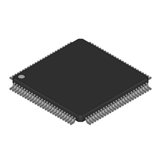
Pin Configurations 100-Pin TQFP
BWS1 BWS0 CE1 CE2 CE3 VDD VSS CEN CLK WE ADV/LD OE NC NC NC A6 A7 NC A8 A9 81 80 79 78 77 76 75 74 73 72 71 70 69 68 67 66 65 64 63 62 61 60 59 58 57 56 55 54 53 52 51 43 44 45 46 47 48 49 50
CY7C1353B
100
99
98
97
96
95
94
93
92
91
90
89
88
87
86
85
84
83
NC NC NC VDDQ VSS NC NC DQ8 DQ9 VSS VDDQ DQ10 DQ11 VSS VDD VDD VSS DQ12 DQ13 VDDQ VSS DQ14 DQ15 DP1 NC VSS VDDQ NC NC NC
1 2 3 4 5 6 7 8 9 10 11 12 13 14 15 16 17 18 19 20 21 22 23 24 25 26 27 28 29 30 31 32 33 34 35 36 37 38
82
CY7C1353B
A17 NC NC VDDQ VSS NC DP0 DQ7 DQ6 VSS VDDQ DQ5 DQ4 VSS VSS VDD VSS DQ3 DQ2 VDDQ VSS DQ1 DQ0 NC NC VSS VDDQ NC NC NC
39
40
41
42
A11
A12
A13
VSS
DNU
VDD
MODE
DNU
DNU
Document #: 38-05266 Rev. **
DNU
A10
A14
A15
A16
A5
A4
A3
A2
A1
A0
Page 2 of 15
�PRELIMINARY
Pin Configurations (continued)
119-Ball BGA 1 A B C D E F G H J K L M N P R T U VDDQ NC NC DQc DQc VDDQ DQc DQc VDDQ DQd DQd VDDQ DQd DQd NC NC VDDQ 2 A CE2 A DQPc DQc DQc DQc DQc VDD DQd DQd DQd DQd DQPd A NC TMS 3 A A A VSS VSS VSS BWc VSS NC VSS BWd VSS VSS VSS MODE A TDI 4 ADSP ADSC VDD NC CE1 OE ADV GW VDD CLK NC BWE A1 A0 VDD A TCK 5 A A A VSS VSS VSS BWb VSS NC VSS BWa VSS VSS VSS VDD A TDO 6 A CE3 A DQPb DQb DQb DQb DQb VDD DQa DQa DQa DQa DQPa A NC NC 7 VDDQ NC NC DQb DQb VDDQ DQb DQb VDDQ DQa DQa VDDQ DQa DQa NC ZZ VDDQ
CY7C1353B
ó
Introduction
Pin Definitions
Pin Number 80, 50−44, 81−82, 99– 100, 32−37 94, 93 Name A[17:0] I/O InputSynchronous InputSynchronous InputSynchronous InputSynchronous Description Address Inputs used to select one of the 262,144 address locations. Sampled at the rising edge of the CLK. Byte Write Select Inputs, active LOW. Qualified with WE to conduct writes to the SRAM. Sampled on the rising edge of CLK. BWS0 controls DQ[7:0] and DP0, BWS1 controls DQ[15:8] and DP1. See Write Cycle Description table for details. Write Enable Input, active LOW. Sampled on the rising edge of CLK if CEN is active LOW. This signal must be asserted LOW to initiate a write sequence. Advance/Load Input used to advance the on-chip address counter or load a new address. When HIGH (and CEN is asserted LOW) the internal burst counter is advanced. When LOW, a new address can be loaded into the device for an access. After being deselected, ADV/LD should be driven LOW in order to load a new address. Clock Input. Used to capture all synchronous inputs to the device. CLK is qualified with CEN. CLK is only recognized if CEN is active LOW. Chip Enable 1 Input, active LOW. Sampled on the rising edge of CLK. Used in conjunction with CE2, and CE3 to select/deselect the device. Chip Enable 2 Input, active HIGH. Sampled on the rising edge of CLK. Used in conjunction with CE1 and CE3 to select/deselect the device. Chip Enable 3 Input, active LOW. Sampled on the rising edge of CLK. Used in conjunction with CE and CE2 to select/deselect the device.
BWS[1:0]
88 85
WE ADV/LD
89 98 97 92
CLK CE1 CE2 CE3
Input-Clock InputSynchronous InputSynchronous InputSynchronous
Document #: 38-05266 Rev. **
Page 3 of 15
�PRELIMINARY
Pin Definitions (continued)
Pin Number 86 Name OE I/O InputAsynchronous
CY7C1353B
87
CEN
InputSynchronous
23−22, DQ[15:0] 19−18, 13−12, 9−8, 73−72, 69−68, 63−62, 59−58
I/OSynchronous
24, 74
DP[1:0]
I/OSynchronous Input Strap pin
31
Mode
15, 16, 41, 65, 91 4, 11, 20, 27, 54, 61, 70, 77 5, 10, 14, 17, 21, 26, 40, 55, 60, 64, 66−67, 71, 76, 90 1−3, 6−7, 25, 28−30,51−53, 56−57, 75, 78−79, 95−96 83, 84
VDD VDDQ VSS
Power Supply I/O Power Supply Ground
Description Output Enable, active LOW. Combined with the synchronous logic block inside the device to control the direction of the I/O pins. When LOW, the I/O pins are allowed to behave as outputs. When deasserted HIGH, I/O pins are three-stated, and act as input data pins. OE is masked during the data portion of a write sequence, during the first clock when emerging from a deselected state, when the device has been deselected. Clock Enable Input, active LOW. When asserted LOW the Clock signal is recognized by the SRAM. When deasserted HIGH the Clock signal is masked. Since deasserting CEN does not deselect the device, CEN can be used to extend the previous cycle when required. Bidirectional Data I/O Lines. As inputs, they feed into an on-chip data register that is triggered by the rising edge of CLK. As outputs, they deliver the data contained in the memory location specified by A[17:0] during the previous clock rise of the read cycle. The direction of the pins is controlled by OE and the internal control logic. When OE is asserted LOW, the pins can behave as outputs. When HIGH, DQ[15:0] are placed in a three-state condition. The outputs are automatically three-stated during the data portion of a write sequence, during the first clock when emerging from a deselected state, and when the device is deselected, regardless of the state of OE. Bidirectional Data Parity I/O Lines. Functionally, these signals are identical to DQ[15:0]. During write sequences, DP0 is controlled by BWS0 and DP1 is controlled by BWS1. Mode Input. Selects the burst order of the device. Tied HIGH selects the interleaved burst order. Pulled LOW selects the linear burst order. MODE should not change states during operation. When left floating MODE will default HIGH, to an interleaved burst order. Power supply inputs to the core of the device. Should be connected to 3.3V power supply. Power supply for the I/O circuitry. Should be connected to a 3.3V power supply. Ground for the device. Should be connected to ground of the system.
NC
-
No Connects. These pins are not connected to the internal device.
NC
-
38, 39, 42, 43 DNU Functional Overview
No Connects. Reserved for address inputs for depth expansion. Pin 83 will be used for 512K depth and pin 84 will be used for 1-Mb depth. Do Not Use Pins. These pins should be left floating or tied to VSS. tus of the Write Enable (WE). BWS[1:0] can be used to conduct byte write operations. Write operations are qualified by the Write Enable (WE). All writes are simplified with on-chip synchronous self-timed write circuitry. Three synchronous Chip Enables (CE1, CE2, CE3) and an asynchronous Output Enable (OE) simplify depth expansion. All operations (Reads, Writes, and Deselects) are pipelined. ADV/LD should be driven LOW once the device has been deselected in order to load a new address for the next operation. Single Read Accesses A read access is initiated when the following conditions are satisfied at clock rise: (1) CEN is asserted LOW, (2) CE1, CE2, Page 4 of 15
The CY7C1353B is a synchronous flow-through burst SRAM designed specifically to eliminate wait states during Write-Read transitions. All synchronous inputs pass through input registers controlled by the rising edge of the clock. The clock signal is qualified with the Clock Enable input signal (CEN). If CEN is HIGH, the clock signal is not recognized and all internal states are maintained. All synchronous operations are qualified with CEN. Maximum access delay from the clock rise (tCDV) is 7.5 ns (117-MHz device). Accesses can be initiated by asserting all three Chip Enables (CE1, CE2, CE3) active at the rising edge of the clock. If Clock Enable (CEN) is active LOW and ADV/LD is asserted LOW, the address presented to the device will be latched. The access can either be a read or write operation, depending on the staDocument #: 38-05266 Rev. **
�PRELIMINARY
and CE3 are ALL asserted active, (3) the Write Enable input signal WE is deasserted HIGH, and 4) ADV/LD is asserted LOW. The address presented to the address inputs (A[17:0]) is latched into the Address Register and presented to the memory core and control logic. The control logic determines that a read access is in progress and allows the requested data to propagate to the output buffers. The data is available within 7.5 ns (117-MHz device) provided OE is active LOW. After the first clock of the read access the output buffers are controlled by OE and the internal control logic. OE must be driven LOW in order for the device to drive out the requested data. On the subsequent clock, another operation (Read/Write/Deselect) can be initiated. When the SRAM is deselected at clock rise by one of the chip enable signals, its output will be three-stated immediately. Burst Read Accesses The CY7C1353B has an on-chip burst counter that allows the user the ability to supply a single address and conduct up to four Reads without reasserting the address inputs. ADV/LD must be driven LOW in order to load a new address into the SRAM, as described in the Single Read Access section above. The sequence of the burst counter is determined by the MODE input signal. A LOW input on MODE selects a linear burst mode, a HIGH selects an interleaved burst sequence. Both burst counters use A0 and A1 in the burst sequence, and will wrap around when incremented sufficiently. A HIGH input on ADV/LD will increment the internal burst counter regardless of the state of chip enable inputs or WE. WE is latched at the beginning of a burst cycle. Therefore, the type of access (Read or Write) is maintained throughout the burst sequence. Single Write Accesses Write access are initiated when the following conditions are satisfied at clock rise: (1) CEN is asserted LOW, (2) CE1, CE2, and CE3 are ALL asserted active, and (3) the write signal WE is asserted LOW. The address presented to A[17:0] is loaded into the Address Register. The write signals are latched into the Control Logic block. The data lines are automatically
CY7C1353B
three-stated regardless of the state of the OE input signal. This allows the external logic to present the data on DQ[15:0] and DP[1:0]. On the next clock rise the data presented to DQ[15:0] and DP[1:0] (or a subset for byte write operations, see Write Cycle Description table for details) inputs is latched into the device and the write is complete. Additional accesses (Read/Write/Deselect) can be initiated on this cycle. The data written during the Write operation is controlled by BWS[1:0] signals. The CY7C1353B provides byte write capability that is described in the Write Cycle Description table. Asserting the Write Enable input (WE) with the selected Byte Write Select (BWS[1:0]) input will selectively write to only the desired bytes. Bytes not selected during a byte write operation will remain unaltered. A synchronous self-timed write mechanism has been provided to simplify the write operations. Byte write capability has been included in order to greatly simplify Read/Modify/Write sequences, which can be reduced to simple byte write operations. Because the CY7C1353B is a common I/O device, data should not be driven into the device while the outputs are active. The Output Enable (OE) can be deasserted HIGH before presenting data to the DQ[15:0] and DP[1:0] inputs. Doing so will three-state the output drivers. As a safety precaution, DQ[15:0] and DP[1:0].are automatically three-stated during the data portion of a write cycle, regardless of the state of OE. Burst Write Accesses The CY7C1353B has an on-chip burst counter that allows the user the ability to supply a single address and conduct up to four Write operations without reasserting the address inputs. ADV/LD must be driven LOW in order to load the initial address, as described in the Single Write Access section above. When ADV/LD is driven HIGH on the subsequent clock rise, the Chip Enables (CE1, CE2, and CE3) and WE inputs are ignored and the burst counter is incremented. The correct BWS[1:0] inputs must be driven in each cycle of the burst write in order to write the correct bytes of data.
Document #: 38-05266 Rev. **
Page 5 of 15
�PRELIMINARY
Cycle Description Truth Table[1, 2, 3, 4, 5, 6]
Operation Deselected Suspend Begin Read Begin Write Burst READ Operation Address used External External External Internal CE 1 X 0 0 X CEN 0 1 0 0 0 ADV/ LD L X 0 0 1 WE X X 1 0 X BWSx X X X Valid X CLK L-H L-H L-H L-H L-H
CY7C1353B
Comments I/Os three-state following next recognized clock. Clock Ignored, all operations suspended. Address Latched. Address Latched, data presented two valid clocks later. Burst Read Operation. Previous access was a Read operation. Addresses incremented internally in conjunction with the state of Mode. Burst Write Operation. Previous access was a Write operation. Addresses incremented internally in conjunction with the state of Mode. Bytes written are determined by BWS[1:0].
Burst WRITE Operation
Internal
X
0
1
X
Valid
L-H
Interleaved Burst Sequence
First Address Ax+1, Ax 00 01 10 11 Second Address Ax+1, Ax 01 00 11 10 Third Address Ax+1, Ax 10 11 00 01 Fourth Address Ax+1, Ax 11 10 01 00
Linear Burst Sequence
First Address Ax+1, Ax 00 01 10 11 Second Address Ax+1, Ax 01 10 11 00 Third Address Ax+1, Ax 10 11 00 01 Fourth Address Ax+1, Ax 11 00 01 10
Write Cycle Description[1, 2]
Function Read Write - No bytes written Write Byte 0 - (DQ[7:0] and DP0) Write Byte 1 - (DQ[15:8] and DP1) Write All Bytes WE 1 0 0 0 0 BWS1 X 1 1 0 0 BWS0 X 1 0 1 0
Notes: 1. X = “Don't Care,” 1 = Logic HIGH, 0 = Logic LOW, CE stands for ALL Chip Enables active. BWSx = 0 signifies at least one Byte Write Select is active, BWSx = Valid signifies that the desired byte write selects are asserted, see Write Cycle Description table for details. 2. Write is defined by WE and BWS[1:0]. See Write Cycle Description table for details. 3. The DQ and DP pins are controlled by the current cycle and the OE signal. 4. CEN=1 inserts wait states. 5. Device will power-up deselected and the I/Os in a three-state condition, regardless of OE. 6. OE assumed LOW.
Document #: 38-05266 Rev. **
Page 6 of 15
�PRELIMINARY
Maximum Ratings
(Above which the useful life may be impaired. For user guidelines, not tested.) Storage Temperature ..................................... −65°C to +150°C Ambient Temperature with Power Applied .................................................. −55°C to +125°C Supply Voltage on VDD Relative to GND ......... −0.5V to +4.6V DC Voltage Applied to Outputs in High Z State[7] ..................................... −0.5V to VDDQ + 0.5V DC Input Voltage[7] .................................. −0.5V to VDDQ + 0.5V
CY7C1353B
Current into Outputs (LOW) ........................................ 20 mA Static Discharge Voltage .......................................... >2001V (per MIL-STD-883, Method 3015) Latch-Up Current.................................................... >200 mA
Operating Range
Range Com’l Ambient Temperature[8] 0°C to +70°C VDD/VDDQ 3.3V ±5%
Electrical Characteristics Over the Operating Range
Parameter VDD VDDQ VOH VOL VIH VIL IX IOZ ICC Description Power Supply Voltage I/O Supply Voltage Output HIGH Voltage Output LOW Voltage Input HIGH Voltage Input LOW Voltage Input Load Current Input Current of MODE Output Leakage Current VDD Operating Supply GND ≤ VI ≤ VDDQ, Output Disabled VDD = Max., IOUT = 0 mA, f = fMAX = 1/tCYC 8.5-ns cycle, 117 MHz 10-ns cycle, 100 MHz 15-ns cycle, 66 MHz 20-ns cycle, 50 MHz 25-ns cycle, 40 MHz ISB1 Automatic CE Power-Down Current—TTL Inputs Max. VDD, Device Deselected, VIN ≥ VIH or VIN ≤ VIL f = fMAX = 1/tCYC 8.5-ns cycle, 117 MHz 10-ns cycle, 100 MHz 15-ns cycle, 66 MHz 20-ns cycle, 50 MHz 25-ns cycle, 40 MHz ISB2 Automatic CE Power-Down Current—CMOS Inputs Automatic CE Power-Down Current—CMOS Inputs Max. VDD, Device Deselected, VIN ≤ 0.3V or VIN > VDDQ − 0.3V, f=0 Max. VDD, Device Deselected, or VIN ≤ 0.3V or VIN > VDDQ − 0.3V f = fMAX = 1/tCYC All speed grades
[7]
Test Conditions
Min. 3.135 3.135
Max. 3.465 3.465 0.4
Unit V V V V V V mA mA mA mA mA mA mA mA mA mA mA mA mA mA
VDD = Min., IOH = –4.0 mA VDD = Min., IOL = 8.0 mA
[9]
2.4 2.0 −0.3 VDD +0.3V 0.8 5 30 5 375 350 250 200 175 90 80 60 40 30 5
[9]
GND ≤ VI ≤ VDDQ
−5 −30 −5
ISB3
8.5-ns cycle, 117 MHz 10-ns cycle, 100 MHz 15-ns cycle, 66 MHz 20-ns cycle, 50 MHz 25-ns cycle, 40 MHz
80 70 50 40 30
mA mA mA mA mA
Notes: 7. Minimum voltage equals −2.0V for pulse duration less than 20 ns. 8. TA is the case temperature. 9. The load used for VOH and VOL testing is shown in figure (b) of the AC Test Loads.
Document #: 38-05266 Rev. **
Page 7 of 15
�PRELIMINARY
Capacitance[10]
Parameter CIN CCLK CI/O Description Input Capacitance Clock Input Capacitance Input/Output Capacitance Test Conditions TA = 25°C, f = 1 MHz, VDD = 3.3V VDDQ = 3.3V Max. 4 4 4
CY7C1353B
Unit pF pF pF
AC Test Loads and Waveforms
R=317Ω ALL INPUT PULSES 3.0V 5 pF INCLUDING JIG AND SCOPE R=351Ω GND
[11]
OUTPUT Z0 =50Ω RL =50Ω VL = 1.5V
3.3V OUTPUT
(a)
(b)
Thermal Resistance
Description Thermal Resistance (Junction to Ambient) Thermal Resistance (Junction to Case) Test Conditions Still Air, soldered on a 4.25 x 1.125 inch, 4-layer printed circuit board. Symbol ΘJA ΘJC TQFP Typ. 28 4 Units °C/W °C/W Notes 10 10
Notes: 10. Tested initially and after any design or process change that may affect these parameters. 11. Unless otherwise noted, test conditions assume signal transition time of 2 ns or less, timing reference levels of 1.5V, input pulse levels of 0 to 3.0V, and output loading shown in (a) of AC Test Loads.
Document #: 38-05266 Rev. **
Page 8 of 15
�PRELIMINARY
Switching Characteristics Over the Operating Range[11, 12, 13]
-117 Parameter tCYC FMAX tCH tCL tAS tAH tCDV tDOH tCENS tCENH tWES tWEH tALS tALH tDS tDH tCES tCEH tCHZ tCLZ tEOHZ tEOLZ tEOV Description Clock Cycle Time Maximum Operating Frequency Clock HIGH Clock LOW Address Set-Up Before CLK Rise Address Hold After CLK Rise Data Output Valid After CLK Rise Data Output Hold After CLK Rise CEN Set-Up Before CLK Rise CEN Hold After CLK Rise WE, BWS[1:0] Set-Up Before CLK Rise WE, BWS[1:0] Hold After CLK Rise ADV/LD Set-Up Before CLK Rise ADV/LD Hold after CLK Rise Data Input Set-Up Before CLK Rise Data Input Hold After CLK Rise Chip Select Set-Up Chip Select Hold After CLK Rise Clock to High-Z Clock to Low-Z
13, 14] [10, 12, 13, 14]
CY7C1353B
-100 Min. 10 Max.
-66 Min. 15.0 Max.
-50 Min. 20.0 66 50 6.0 6.0 2.0 1.0 11 12.0 1.5 2.0 1.0 2.0 1.0 2.0 1.0 2.0 1.0 2.0 1.0 5.0 1.5 3.0 6.0 7.0 0 6.0 7.0 0 5.0 1.5 2.5 1.0 2.5 1.0 2.5 1.0 2.5 1.0 2.5 1.0 1.5 3.0 7.0 7.0 2.5 1.0 Max.
-40 Min. 25.0 40 Max. Unit ns MHz ns ns ns ns 14.0 ns ns ns ns ns ns ns ns ns ns ns ns 5.0 ns ns 8.0 ns ns 8.0 ns
Min. 8.5
Max.
117 1.9 1.9 2.0 0.5 7.5 1.5 2.0 0.5 2.0 0.5 2.0 0.5 2.0 0.5 2.0 0.5 1.5 3.0 4.2 0 4.2 0 4.2 1.5 2.0 0.5 2.0 0.5 2.0 0.5 2.0 0.5 2.0 0.5 1.5 3.0 1.9 1.9 2.0 0.5
100 5.0 5.0 2.0 0.5 8.5 1.5 2.0 0.5 2.0 0.5 2.0 0.5 2.0 0.5 2.0 0.5 5.0 1.5 3.0 5.0 0 5.0
[10, 12, 13, 14] [10, 12,
OE HIGH to Output High-Z
OE LOW to Output Low-Z[10, 12, 13,
14]
OE LOW to Output Valid[12]
Note: 12. tCHZ, tCLZ, tOEV, tEOLZ, and tEOHZ are specified with AC test conditions shown in part (a) of AC Test Loads. Transition is measured ± 200 mV from steady-state voltage. 13. At any given voltage and temperature, tEOHZ is less than tEOLZ and tCHZ is less than tCLZ to eliminate bus contention between SRAMs when sharing the same data bus. These specifications do not imply a bus contention condition, but reflect parameters guaranteed over worst case user conditions. Device is designed to achieve High-Z prior to Low-Z under the same system conditions. 14. This parameter is sampled and not 100% tested.
Document #: 38-05266 Rev. **
Page 9 of 15
�PRELIMINARY
CY7C1353B
Switching Waveforms
Read/Write Waveforms
DESELECT Write Read
DESELECT
CLK
tCENS tCENH tCH tCL tCYC tCENS tCENH
CEN
tAS
ADDRESS
RA1
WA2
RA3
RA4
WA5
RA6
RA7
tAH
WE
tWS tWH tCES
tCEH
CE
tCHZ D2 In Q3 Out tDOH tCHZ Q4 Out D5 In Q6 Out Q7 Out
tCLZ
tDOH Q1 Out tCDV
DataIn/Out
Device originally deselected
WE is the combination of WE & BWSx to define a Write Cycle (see Write Cycle Description table). CE is the combination of CE1, CE2, and CE3. All Chip Selects need to be active in order to select the device. Any Chip Select can deselect the device. RAx stands for Read Address X, WAx stands for Write Address X, Dx stands for Data-in X, Qx stands for Data-out X.
= DON’T CARE
= UNDEFINED
Document #: 38-05266 Rev. **
Page 10 of 15
DESELECT
Suspend
Read
Read
Write
Read
Read
�PRELIMINARY
Switching Waveforms
Begin Read Burst Read Burst Read
CY7C1353B
Burst Sequences
Burst Read
Begin Read
Begin Write
Burst Write
CLK
tALS tALH tCH tCL tCYC
ADV/LD
tAS tAH
ADDRESS
RA1
WA2
Burst Write
Burst Write
RA3
WE
tWS tWH tWS tWH
BWS[1:0]
tCES tCEH
CE
tDOH Q1 1a Out tCDV Q1+1 Out Q1+2 Out tCHZ Q1+3 Out tDS tDH D2 In D2+1 In D2+2 In tCLZ D2+3 In Q3 Out Q3+1 Out
tCLZ
DataIn/Out
tCDV Device originally deselected
The combination of WE & BWS[1:0] defines a write cycle (see Write Cycle Description table). CE is the combination of CE1, CE2, and CE3. All Chip Enables need to be active in order to select the device. Any Chip Enable can deselect the device. RAx stands for Read Address X, WAx stands for Write Address X, Dx stands for Data-in for location X, Qx stands for Data-out for location X. CEN held LOW. During burst writes, byte writes can be conducted by asserting the appropriate BWS[1:0] input signals. Burst order determined by the state of the MODE input. CEN held LOW. OE held LOW. = DON’T CARE = UNDEFINED
Document #: 38-05266 Rev. **
Burst Read
Page 11 of 15
Burst Read
�PRELIMINARY
Switching Waveforms
OE Timing
CY7C1353B
OE
tEOHZ tEOV
I/O’s
Three-state
tEOLZ
Ordering Information
Speed (MHz) 117 100 66 Ordering Code CY7C1353B-117AC CY7C1353B-100AC CY7C1353B-66AC CY7C1353B-66BGC 50 CY7C1353B-50AC CY7C1353B-50BGC 40 CY7C1353B-40AC Package Name A101 A101 A101 BG119 A101 BG119 A101 Package Type 100-Lead 14 x 20 x 1.4 mm Thin Quad Flat Pack 100-Lead 14 x 20 x 1.4 mm Thin Quad Flat Pack 100-Lead 14 x 20 x 1.4 mm Thin Quad Flat Pack 119-Lead FBGA (14 x 22 x 2.4 mm) 100-Lead 14 x 20 x 1.4 mm Thin Quad Flat Pack 119-Lead FBGA (14 x 22 x 2.4 mm) 100-Lead 14 x 20 x 1.4 mm Thin Quad Flat Pack Operating Range Commercial Commercial Commercial Commercial Commercial Commercial Commercial
Shaded areas contain advance information.
Document #: 38-05266 Rev. **
Page 12 of 15
�PRELIMINARY
CY7C1353B
Package Diagrams
100-Pin Thin Plastic Quad Flatpack (14 x 20 x 1.4 mm) A101
51-85050-A
Document #: 38-05266 Rev. **
Page 13 of 15
�PRELIMINARY
Package Diagrams (continued)
CY7C1353B
119-Lead PBGA (14 x 22 x 2.4 mm) BG119
51-85115-*A
Document #: 38-05266 Rev. **
Page 14 of 15
© Cypress Semiconductor Corporation, 2002. The information contained herein is subject to change without notice. Cypress Semiconductor Corporation assumes no responsibility for the use of any circuitry other than circuitry embodied in a Cypress Semiconductor product. Nor does it convey or imply any license under patent or other rights. Cypress Semiconductor does not authorize its products for use as critical components in life-support systems where a malfunction or failure may reasonably be expected to result in significant injury to the user. The inclusion of Cypress Semiconductor products in life-support systems application implies that the manufacturer assumes all risk of such use and in doing so indemnifies Cypress Semiconductor against all charges.
�PRELIMINARY
CY7C1353B
Document Title: CY7C1353B 256Kx18 Flow-Through SRAM with NoBL™ Architecture Document Number: 38-05266 REV. ** ECN NO. 114137 Issue Date 03/18/02 Orig. of Change DSG Description of Change Change from Spec number: 38-00950 to 38-05266
Document #: 38-05266 Rev. **
Page 15 of 15
�