327
CY7C1359A/GVT71256T18
256K x 18 Synchronous-Pipelined Cache Tag RAM
Features
•
•
•
•
•
•
•
•
•
•
•
•
•
•
•
•
•
•
•
Fast match times: 3.5, 3.8, 4.0 and 4.5 ns
Fast clock speed: 166, 150, 133, and 100 MHz
Fast OE access times: 3.5, 3.8, 4.0 and 5.0 ns
Pipelined data comparator
Data input register load control by DEN
Optimal for depth expansion (one cycle chip deselect
to eliminate bus contention)
3.3V –5% and +10% core power supply
2.5V or 3.3V I/O supply
5V tolerant inputs except I/Os
Clamp diodes to VSS at all inputs and outputs
Common data inputs and data outputs
JTAG boundary scan
Byte Write Enable and Global Write control
Three chip enables for depth expansion and address
pipeline
Address, data, and control registers
Internally self-timed Write Cycle
Burst control pins (interleaved or linear burst sequence)
Automatic power-down for portable applications
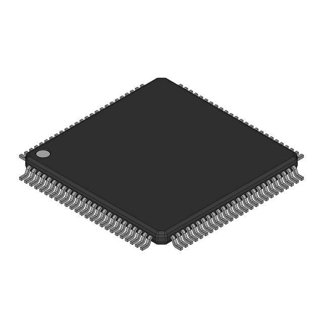
Low-profile JEDEC standard 100-pin TQFP package
Functional Description
The Cypress Synchronous Burst SRAM family employs
high-speed, low power CMOS designs using advanced triple-layer polysilicon, double-layer metal technology. Each
memory cell consists of four transistors and two high valued
resistors.
All synchronous inputs are gated by registers controlled by a
positive-edge-triggered Clock Input (CLK). The synchronous
inputs include all addresses, all data inputs, address-pipelining Chip Enable (CE), depth-expansion Chip Enables (CE2
and CE2), Burst Control Inputs (ADSC, ADSP, and ADV), Write
Enables (WEL, WEH, and BWE), Global Write (GW), and Data
Input Enable (DEN).
Asynchronous inputs include the Burst Mode Control (MODE),
the Output Enable (OE) and the Match Output Enable (MOE).
The data outputs (Q) and Match Output (MATCH), enabled by
OE and MOE respectively, are also asynchronous.
Addresses and chip enables are registered with either Address Status Processor (ADSP) or Address status Controller
(ADSC) input pins. Subsequent burst addresses can be internally generated as controlled by the Burst Advance pin (ADV).
Data inputs are registered with Data Input Enable (DEN) and
chip enable pins (CE, CE2, and CE2). The outputs of the data
input registers are compared with data in the memory array
and a match signal is generated. The match output is gated
into a pipeline register and released to the match output pin at
the next rising edge of Clock (CLK).
Address, data inputs, and write controls are registered on-chip
to initiate self-timed WRITE cycle. WRITE cycles can be one
to two bytes wide as controlled by the write control inputs. Individual byte write allows individual byte to be written. WEL
controls DQ1–DQ9. WEH controls DQ10–DQ18. WEL and
WEH can be active only with BWE being LOW. GW being LOW
causes all bytes to be written.
The CY7C1359C/GVT71256T18 operates from a +3.3V power supply with output power supply being +2.5V or +3.3V. All
inputs and outputs are LVTTL compatible. The device is ideally
suited for address tag RAM for up to 8 MB secondary cache.
Selection Guide
7C1359A-166
71256T36-6
7C1359A-150
71256T36-6.7
7C1359A-133
71256T36-7.5
7C1359A-100
71256T36-10
Maximum Access Time (ns)
3.5
3.8
4.0
4.5
Maximum Operating Current (mA)
310
275
250
190
Maximum CMOS Standby Current (mA)
20
20
20
20
Cypress Semiconductor Corporation
Document #: 38-05120 Rev. *A
•
3901 North First Street
•
San Jose
•
CA 95134 • 408-943-2600
Revised January 19, 2003
�CY7C1359A/GVT71256T18
Functional Block Diagram—256Kx18[1]
HIGHER BYTE
WRITE
WEH#
BWE#
D
Q
D
Q
LOWER BYTE
WRITE
D
Q
CE#
lo byte write
GW#
ENABLE
CE2
Latch
D
Q
D
Q
hi byte write
WEL#
CE2#
ZZ
Power Down Logic
OE#
D
ADSP#
Q
MATCH
MOE#
Compare
Input
Register
DEN#
Latch
CLK
16
Address
Register
CLR
ADV#
A1-A0
Binary
Counter
& Logic
OUTPUT
REGISTER
D
Q
Output Buffers
ADSC#
256K x 9 x 2
SRAM Array
A
DQ1DQ18
MODE
Note:
1. The Functional Block Diagram illustrates simplified device operation. See Truth Table, pin descriptions and timing diagrams for detailed information.
Document #: 38-05120 Rev. *A
Page 2 of 24
�CY7C1359A/GVT71256T18
Pin Configurations
100
99
98
97
96
95
94
93
92
91
90
89
88
87
86
85
84
83
82
81
A
A
CE
CE2
NC
NC
WEH
WEL
CE2
VCC
VSS
CLK
GW
BWE
OE
ADSC
ADSP
ADV
A
A
100-Pin TQFP
Top View
NC
NC
NC
CY7C1359A/GVT71256T18
80
79
78
77
76
75
74
73
72
71
70
69
68
67
66
65
64
63
62
61
60
59
58
57
56
55
54
53
52
51
A
NC
NC
VCCQ
VSSQ
NC
DQ9
DQ8
DQ7
VSSQ
VCCQ
DQ6
DQ5
VSS
NC
VCC
ZZ
DQ4
DQ3
VCCQ
VSSQ
DQ2
DQ1
NC
NC
VSSQ
VCCQ
MATCH
DEN
MOE
MODE
A
A
A
A
A1
A0
TMS
TDI
VSS
VCC
TDO
TCK
A
A
A
A
A
A
A
31
32
33
34
35
36
37
38
39
40
41
42
43
44
45
46
47
48
49
50
VCCQ
VSSQ
NC
NC
DQ10
DQ11
VSSQ
VCCQ
DQ12
DQ13
NC
VCC
NC
VSS
DQ14
DQ15
VCCQ
VSSQ
DQ16
DQ17
DQ18
NC
VSSQ
VCCQ
NC
NC
NC
1
2
3
4
5
6
7
8
9
10
11
12
13
14
15
16
17
18
19
20
21
22
23
24
25
26
27
28
29
30
119-Lead BGA
Top View
1
2
3
4
5
6
7
A
VCCQ
A
A
ADSP
A
A
VCCQ
B
NC
CE2
A
ADSC
A
CE2
NC
C
NC
A
A
VCC
A
A
NC
D
DQ10
NC
VSS
NC
VSS
DQ9
NC
E
NC
DQ11
VSS
CE
VSS
NC
DQ8
F
VCCQ
NC
VSS
OE
VSS
DQ7
VCCQ
G
NC
DQ12
WEH
ADV
VSS
NC
DQ6
H
DQ13
NC
VSS
GW
VSS
DQ5
NC
J
VCCQ
VCC
NC
VCC
NC
VCC
VCCQ
K
NC
DQ14
VSS
CLK
VSS
NC
DQ4
L
DQ15
NC
VSS
NC
WEL
DQ3
NC
M
VCCQ
DQ16
VSS
BWE
VSS
MATCH
VCCQ
N
DQ17
NC
VSS
A1
VSS
DQ2
DEN
P
NC
DQ18
VSS
A0
VSS
MOE
DQ1
R
NC
A
MODE
VCC
NC
A
NC
T
NC
A
A
NC
A
A
ZZ
U
VCCQ
TMS
TDI
TCK
TDO
NC
VCCQ
Document #: 38-05120 Rev. *A
Page 3 of 24
�CY7C1359A/GVT71256T18
Pin Descriptions
BGA Pins
TQFP Pins
Name
Type
Description
4P
4N
2A, 3A, 5A, 6A,
3B, 5B, 2C, 3C,
5C, 6C, 2R, 6R,
2T, 3T, 5T, 6T
37
36
35, 34, 33, 32,
100, 99, 82, 81,
80, 48, 47, 46, 45,
44, 49, 50
A0
A1
A
InputSynchronous
Addresses: These inputs are registered and must meet the
set-up and hold times around the rising edge of CLK. The
burst counter generates internal addresses associated with
A0 and A1, during burst cycle and wait cycle.
5L
3G
93
94
WEL
WEH
InputSynchronous
Byte Write Enables: A byte write enable is LOW for a WRITE
cycle and HIGH for a READ cycle. WEL controls DQ1–DQ9.
WEH controls DQ10–DQ18. Data I/O are high impedance if
either of these inputs are LOW, conditioned by BWE being
LOW.
4M
87
BWE
InputSynchronous
Write Enable: This active LOW input gates byte write operations and must meet the set-up and hold times around the
rising edge of CLK.
4H
88
GW
InputSynchronous
Global Write: This active LOW input allows a full 18-bit
WRITE to occur independent of the BWE and WEn lines and
must meet the set-up and hold times around the rising edge
of CLK.
4K
89
CLK
InputSynchronous
Clock: This signal registers the addresses, data, chip enables, write control, and data input enable control input on its
rising edge. All synchronous inputs must meet set-up and
hold times around the clock’s rising edge.
4E
98
CE
InputSynchronous
Chip Enable: This active LOW input is used to enable the
device and to gate ADSP.
6B
92
CE2
InputSynchronous
Chip Enable: This active LOW input is used to enable the
device.
2B
97
CE2
inputSynchronous
Chip Enable: This active HIGH input is used to enable the
device.
4F
86
OE
Input
Output Enable: This active LOW asynchronous input enables
the data output drivers.
4G
83
ADV
InputSynchronous
Address Advance: This active LOW input is used to control
the internal burst counter. A HIGH on this pin generates wait
cycle (no address advance).
4A
84
ADSP
InputSynchronous
Address Status Processor: This active LOW input, along with
CE being LOW, causes a new external address to be registered and a READ cycle is initiated using the new address.
4B
85
ADSC
InputSynchronous
Address Status Controller: This active LOW input causes device to be deselected or selected along with new external
address to be registered. A READ or WRITE cycle is initiated
depending upon write control inputs.
3R
31
MODE
InputStatic
Mode: This input selects the burst sequence. A LOW on this
pin selects Linear Burst. A NC or HIGH on this pin selects
Interleaved Burst.
7T
64
ZZ
7N
52
DEN
InputSynchronous
Data Input Enable: This active LOW input is used to control
the update of data input registers.
6M
53
MATCH
Output
Match Output: MATCH will be HIGH if data in the data input
registers match the data stored in the memory array, assuming MOE being LOW. MATCH will be LOW if data do not
match.
Document #: 38-05120 Rev. *A
InputSnooze: This active HIGH input puts the device in low power
Asynchronous consumption standby mode. For normal operation, this input
has to be either LOW or NC (No Connect).
Page 4 of 24
�CY7C1359A/GVT71256T18
Pin Descriptions (continued)
BGA Pins
TQFP Pins
Name
Type
Description
6P
51
MOE
Input
Match Output Enable: This active LOW asynchronous input
enables the MATCH output drivers.
7P, 6N, 6L, 7K,
6H, 7G, 6F, 7E,
6D, 1D, 2E, 2G,
1H, 2K, 1L, 2M,
1N, 2P
58, 59, 62, 63, 68,
69, 72, 73, 74, 8,
9, 12, 13, 18, 19,
22, 23, 24
DQ1–
DQ18
Input/
Output
Data Inputs/Outputs: Input data must meet setup and hold
times around the rising edge of CLK.
5U
42
TDO
Output
IEEE 1149.1 test output. LVTTL-level output.
2U
3U
4U
38
39
43
TMS
TDI
TCK
Input
IEEE 1149.1 test inputs. LVTTL-level inputs.
4C, 2J, 4J, 6J, 4R
15, 41,65, 91
VCC
Supply
Power Supply: +3.3V –5% and +10%
3D, 5D, 3E, 5E,
3F, 5F, 5G, 3H,
5H, 3K, 5K, 3L,
3M, 5M, 3N, 5N,
3P, 5P
5, 10, 17, 21, 26,
40, 55, 60, 67, 71,
76, 90
VSS
Ground
Ground: GND
1A, 7A, 1F, 7F, 1J,
7J, 1M, 7M, 1U,
7U
4, 11, 20, 27, 54,
61, 70, 77
VCCQ
I/O Supply
NC
-
1B, 7B, 1C, 7C,
1-3, 6, 7, 14, 16,
2D, 4D, 7D, 1E, 25, 28-30, 56, 57,
6E, 2F, 1G, 6G, 66, 75, 78, 79, 95,
2H, 7H, 3J, 5J,
96
1K, 6K, 2L, 4L,
7L, 2N, 1P, 1R,
5R, 7R, 1T, 4T, 6U
Output Buffer Supply: +2.5V (from 2.375V to VCC)
No Connect: These signals are not internally connected.
Burst Address Table (MODE = GND)
Burst Address Table (MODE = NC/VCC)
First
Address
(external)
Second
Address
(internal)
Third
Address
(internal)
Fourth
Address
(internal)
First
Address
(external)
Second
Address
(internal)
Third
Address
(internal)
Fourth
Address
(internal)
A...A00
A...A01
A...A10
A...A11
A...A00
A...A01
A...A10
A...A11
A...A01
A...A00
A...A11
A...A10
A...A01
A...A10
A...A11
A...A00
A...A10
A...A11
A...A00
A...A01
A...A10
A...A11
A...A00
A...A01
A...A00
A...A11
A...A00
A...A01
A...A10
A...A11
A...A10
A...A01
Partial Truth Table for MATCH[2, 3, 4, 5, 6]
Operation
E
WE
DEN
MOE
OE
MATCH
DQ
READ Cycle
L
H
X
X
L
-
Q
WRITE Cycle
L
L
L
X
H
-
D
Fill WRITE Cycle
L
L
H
X
H
-
High-Z
COMPARE Cycle
L
H
L
L
H
Output
D
Deselected Cycle (MATCH Out)
H
X
X
L
X
H
High-Z
Deselected Cycle
H
X
X
H
X
High-Z
High-Z
Notes:
2. X means “don’t care.” H means logic HIGH. L means logic LOW. It is assumed in this table that ADSP is HIGH and ADSC is LOW.
3. E=L is defined as CE=LOW and CE2=LOW and CE2=HIGH. E =H is defined as CE=HIGH or CE2=HIGH or CE2=LOW. WE is defined as [BWE + WEL*WEH]*GW.
4. All inputs except OE and MOE must meet setup and hold times around the rising edge (LOW to HIGH) of CLK.
5. For a write operation following a read operation, OE must be HIGH before the input data required setup time plus High-Z time for OE and staying HIGH throughout
the input data hold time.
6. This device contains circuitry that will ensure the outputs will be in High-Z during power-up.
Document #: 38-05120 Rev. *A
Page 5 of 24
�CY7C1359A/GVT71256T18
Truth Table[5, 6, 7, 8, 9, 10, 11]
Operation
Address
Used
CE
ADSC
ADV
WRITE
OE
CLK
DQ
Deselected Cycle, Power Down
None
H
X
X
X
L
X
X
X
L-H
High-Z
Deselected Cycle, Power Down
None
L
X
L
L
X
X
X
X
L-H
High-Z
Deselected Cycle, Power Down
None
L
H
X
L
X
X
X
X
L-H
High-Z
Deselected Cycle, Power Down
None
L
X
L
H
L
X
X
X
L-H
High-Z
Deselected Cycle, Power Down
None
L
H
X
H
L
X
X
X
L-H
High-Z
READ Cycle, Begin Burst
External
L
L
H
L
X
X
X
L
L-H
Q
READ Cycle, Begin Burst
External
L
L
H
L
X
X
X
H
L-H
High-Z
WRITE Cycle, Begin Burst
External
L
L
H
H
L
X
L
X
L-H
D
READ Cycle, Begin Burst
External
L
L
H
H
L
X
H
L
L-H
Q
READ Cycle, Begin Burst
External
L
L
H
H
L
X
H
H
L-H
High-Z
READ Cycle, Continue Burst
Next
X
X
X
H
H
L
H
L
L-H
Q
READ Cycle, Continue Burst
Next
X
X
X
H
H
L
H
H
L-H
High-Z
READ Cycle, Continue Burst
Next
H
X
X
X
H
L
H
L
L-H
Q
READ Cycle, Continue Burst
Next
H
X
X
X
H
L
H
H
L-H
High-Z
WRITE Cycle, Continue Burst
Next
X
X
X
H
H
L
L
X
L-H
D
WRITE Cycle, Continue Burst
Next
H
X
X
X
H
L
L
X
L-H
D
READ Cycle, Suspend Burst
Current
X
X
X
H
H
H
H
L
L-H
Q
READ Cycle, Suspend Burst
Current
X
X
X
H
H
H
H
H
L-H
High-Z
READ Cycle, Suspend Burst
Current
H
X
X
X
H
H
H
L
L-H
Q
READ Cycle, Suspend Burst
Current
H
X
X
X
H
H
H
H
L-H
High-Z
WRITE Cycle, Suspend Burst
Current
X
X
X
H
H
H
L
X
L-H
D
WRITE Cycle, Suspend Burst
Current
H
X
X
X
H
H
L
X
L-H
D
CE2 CE2 ADSP
Partial Truth Table for READ/WRITE[12]
Function
GW
BWE
WEH
WEL
READ
H
H
X
X
READ
H
L
H
H
WRITE one byte
H
L
L
H
WRITE all bytes
H
L
L
L
WRITE all bytes
L
X
X
X
Notes:
7. X means “Don’t Care.” H means logic HIGH. L means logic LOW. WRITE = L means [BWE + WEL*WEH]*GW equals LOW. WRITE = H means [BWE +
WEL*WEH]*GW equals HIGH. It is assumed in this truth table that DEN is LOW.
8. WEL enables write to DQ1–DQ9. WEH enables write to DQ10–DQ18.
9. All inputs except OE must meet set-up and hold times around the rising edge (LOW to HIGH) of CLK.
10. Suspending burst generates wait cycle.
11. ADSP LOW along with chip being selected always initiates a READ cycle at the L-H edge of CLK. A WRITE cycle can be performed by setting WRITE LOW for
the CLK L-H edge of the subsequent wait cycle. Refer to WRITE timing diagram for clarification.
12. X means “don’t care.” H means logic HIGH. L means logic LOW. It is assumed in this truth table that chip is selected and ADSP is HIGH along with DEN being LOW.
Document #: 38-05120 Rev. *A
Page 6 of 24
�CY7C1359A/GVT71256T18
IEEE 1149.1 Serial Boundary Scan (JTAG)
Overview
This device incorporates a serial boundary scan access port
(TAP). This port is designed to operate in a manner consistent
with IEEE Standard 1149.1-1990 (commonly referred to as
JTAG), but does not implement all of the functions required for
IEEE 1149.1 compliance. Certain functions have been modified or eliminated because their implementation places extra
delays in the critical speed path of the device. Nevertheless,
the device supports the standard TAP controller architecture
(the TAP controller is the state machine that controls the TAP’s
operation) and can be expected to function in a manner that
does not conflict with the operation of devices with IEEE Standard 1149.1 compliant TAPs. The TAP operates using
LVTTL/LVCMOS logic level signaling.
Disabling the JTAG Feature
It is possible to use this device without using the JTAG feature.
To disable the TAP controller without interfering with normal
operation of the device, TCK should be tied LOW (VSS) to
prevent clocking the device. TDI and TMS are internally pulled
up and may be unconnected. They may alternately be pulled
up to VCC through a resistor. TDO should be left unconnected.
Upon power-up the device will come up in a reset state which
will not interfere with the operation of the device.
Test Access Port (TAP)
TCK - Test Clock (INPUT)
Clocks all TAP events. All inputs are captured on the rising
edge of TCK and all outputs propagate from the falling edge
of TCK.
TMS - Test Mode Select (INPUT)
The TMS input is sampled on the rising edge of TCK. This is
the command input for the TAP controller state machine. It is
allowable to leave this pin unconnected if the TAP is not used.
The pin is pulled up internally, resulting in a logic HIGH level.
TDI - Test Data In (INPUT)
The TDI input is sampled on the rising edge of TCK. This is the
input side of the serial registers placed between TDI and TDO.
The register placed between TDI and TDO is determined by
the state of the TAP controller state machine and the instruction that is currently loaded in the TAP instruction register (refer to Figure 1, TAP Controller State Diagram). It is allowable
to leave this pin unconnected if it is not used in an application.
The pin is pulled up internally, resulting in a logic HIGH level.
TDI is connected to the most significant bit (MSB) of any register. (See Figure 2.)
TDO - Test Data Out (OUTPUT)
The TDO output pin is used to serially clock data-out from the
registers. The output that is active depending on the state of
the TAP state machine (refer to Figure 1, TAP Controller State
Diagram). Output changes in response to the falling edge of
TCK. This is the output side of the serial registers placed between TDI and TDO. TDO is connected to the least significant
bit (LSB) of any register. (See Figure 2.)
Document #: 38-05120 Rev. *A
Performing a TAP Reset
The TAP circuitry does not have a Reset pin (TRST, which is
optional in the IEEE 1149.1 specification). A RESET can be
performed for the TAP controller by forcing TMS HIGH (VCC)
for five rising edges of TCK and pre-loads the instruction register with the IDCODE command. This type of reset does not
affect the operation of the system logic. The reset affects test
logic only.
At power-up, the TAP is reset internally to ensure that TDO is
in a High-Z state.
Test Access Port (TAP) Registers
Overview
The various TAP registers are selected (one at a time) via the
sequences of ones and zeros input to the TMS pin as the TCK
is strobed. Each of the TAP’s registers are serial shift registers
that capture serial input data on the rising edge of TCK and
push serial data out on subsequent falling edge of TCK. When
a register is selected, it is connected between the TDI and
TDO pins.
Instruction Register
The instruction register holds the instructions that are executed by the TAP controller when it is moved into the run test/idle
or the various data register states. The instructions are three
bits long. The register can be loaded when it is placed between
the TDI and TDO pins. The parallel outputs of the instruction
register are automatically preloaded with the IDCODE instruction upon power-up or whenever the controller is placed in the
test-logic reset state. When the TAP controller is in the Capture-IR state, the two least significant bits of the serial instruction register are loaded with a binary “01” pattern to allow for
fault isolation of the board-level serial test data path.
Bypass Register
The bypass register is a single-bit register that can be placed
between TDI and TDO. It allows serial test data to be passed
through the device TAP to another device in the scan chain
with minimum delay. The bypass register is set LOW (VSS)
when the BYPASS instruction is executed.
Boundary Scan Register
The Boundary scan register is connected to all the input and
bidirectional I/O pins (not counting the TAP pins) on the device.
This also includes a number of NC pins that are reserved for
future needs. There are a total of 70 bits for a x36 device and
51 bits for a x18 device. The boundary scan register, under the
control of the TAP controller, is loaded with the contents of the
device I/O ring when the controller is in Capture-DR state and
then is placed between the TDI and TDO pins when the controller is moved to Shift-DR state. The EXTEST, SAMPLE/
PRELOAD and SAMPLE-Z instructions can be used to capture the contents of the I/O ring.
The Boundary Scan Order table describes the order in which
the bits are connected. The first column defines the bit’s position in the boundary scan register. The MSB of the register is
connected to TDI, and LSB is connected to TDO. The second
column is the signal name and the third column is the bump
number. The third column is the TQFP pin number and the
fourth column is the BGA bump number.
Page 7 of 24
�CY7C1359A/GVT71256T18
Identification (ID) Register
The ID Register is a 32-bit register that is loaded with a device
and vendor specific 32-bit code when the controller is put in
Capture-DR state with the IDCODE command loaded in the
instruction register. The register is then placed between the
TDI and TDO pins when the controller is moved into Shift-DR
state. Bit 0 in the register is the LSB and the first to reach TDO
when shifting begins. The code is loaded from a 32-bit on-chip
ROM. It describes various attributes of the device as described
in the Identification Register Definitions table.
TAP Controller Instruction Set
Overview
There are two classes of instructions defined in the IEEE Standard 1149.1-1990; the standard (public) instructions and device specific (private) instructions. Some public instructions
are mandatory for IEEE 1149.1 compliance. Optional public
instructions must be implemented in prescribed ways.
Although the TAP controller in this device follows the IEEE
1149.1 conventions, it is not IEEE 1149.1 compliant because
some of the mandatory instructions are not fully implemented.
The TAP on this device may be used to monitor all input and
I/O pads, but can not be used to load address, data, or control
signals into the device or to preload the I/O buffers. In other
words, the device will not perform IEEE 1149.1 EXTEST, INTEST, or the preload portion of the SAMPLE/PRELOAD command.
When the TAP controller is placed in Capture-IR state, the two
least significant bits of the instruction register are loaded with
01. When the controller is moved to the Shift-IR state the instruction is serially loaded through the TDI input (while the
previous contents are shifted out at TDO). For all instructions,
the TAP executes newly loaded instructions only when the
controller is moved to Update-IR state. The TAP instruction
sets for this device are listed in the following tables.
EXTEST
EXTEST is an IEEE 1149.1 mandatory public instruction. It is
to be executed whenever the instruction register is loaded with
all 0s. EXTEST is not implemented in this device.
The TAP controller does recognize an all-0 instruction. When
an EXTEST instruction is loaded into the instruction register,
the device responds as if a SAMPLE/PRELOAD instruction
has been loaded. There is one difference between two instructions. Unlike SAMPLE/PRELOAD instruction, EXTEST places
the device outputs in a High-Z state.
IDCODE
The IDCODE instruction causes a vendor-specific, 32-bit code
to be loaded into the ID register when the controller is in
Document #: 38-05120 Rev. *A
Capture-DR mode and places the ID register between the TDI
and TDO pins in Shift-DR mode. The IDCODE instruction is
the default instruction loaded in the instruction upon power-up
and at any time the TAP controller is placed in the test-logic
reset state.
SAMPLE-Z
If the High-Z instruction is loaded in the instruction register, all
output pins are forced to a High-Z state and the boundary scan
register is connected between TDI and TDO pins when the
TAP controller is in a Shift-DR state.
SAMPLE/PRELOAD
SAMPLE/PRELOAD is an IEEE 1149.1 mandatory instruction.
The PRELOAD portion of the command is not implemented in
this device, so the device TAP controller is not fully IEEE
1149.1-compliant.
When the SAMPLE/PRELOAD instruction is loaded in the instruction register and the TAP controller is in the Capture-DR
state, a snap shot of the data in the device’s input and I/O
buffers is loaded into the boundary scan register. Because the
device system clock(s) are independent from the TAP clock
(TCK), it is possible for the TAP to attempt to capture the input
and I/O ring contents while the buffers are in transition (i.e., in
a metastable state). Although allowing the TAP to sample
metastable inputs will not harm the device, repeatable results
can not be expected. To guarantee that the boundary scan
register will capture the correct value of a signal, the device
input signals must be stabilized long enough to meet the TAP
controller’s capture setup plus hold time (tCS plus tCH). The
device clock input(s) need not be paused for any other TAP
operation except capturing the input and I/O ring contents into
the boundary scan register.
Moving the controller to Shift-DR state then places the boundary scan register between the TDI and TDO pins. Because the
PRELOAD portion of the command is not implemented in this
device, moving the controller to the Update-DR state with the
SAMPLE/PRELOAD instruction loaded in the instruction register has the same effect as the Pause-DR command.
BYPASS
When the BYPASS instruction is loaded in the instruction register and the TAP controller is in the Shift-DR state, the bypass
register is placed between TDI and TDO. This allows the board
level scan path to be shortened to facilitate testing of other
devices in the scan path.
Reserved
Do not use these instructions. They are reserved for future
use.
Page 8 of 24
�CY7C1359A/GVT71256T18
1
TEST-LOGIC
RESET
0
0
REUN-TEST/
IDLE
1
1
1
SELECT
DR-SCAN
SELECT
IR-SCAN
0
0
1
1
CAPTURE-IR
CAPTURE-DR
0
0
0
SHIFT-DR
0
SHIFT-IR
1
1
1
EXIT1-DR
1
EXIT1-IR
0
0
PAUSE-DR
0
0
PAUSE-IR
1
1
0
0
EXIT2-IR
EXIT2-DR
1
1
UPDATE-DR
1
0
UPDATE-IR
1
0
Figure 1. TAP Controller State Diagram[13]
Note:
13. The 0/1 next to each state represents the value at TMS at the rising edge of TCK.
Document #: 38-05120 Rev. *A
Page 9 of 24
�CY7C1359A/GVT71256T18
0
Bypass Register
Selection
Circuitry
2
TDI
1
0
1
0
1
0
Selection
Circuitry
TDO
Instruction Register
31 30
29
.
.
2
Identification Register
x
.
.
.
.
2
Boundary Scan Register [14]
TDI
TAP Controller
TDI
Figure 2. TAP Controller Block Diagram
TAP DC Electrical Characteristics (20°C < Tj < 110°C; VCC = 3.3V –0.2V and +0.3V unless otherwise noted)
Parameter
VIH
Description
Test Conditions
Input High (Logic 1) Voltage[15, 16]
[15, 16]
Min.
Max.
Unit
2.0
VCC + 0.3
V
–0.3
0.8
V
VIl
Input Low (Logic 0) Voltage
ILI
Input Leakage Current
0V < VIN < VCC
–5.0
5.0
µA
ILO
Output Leakage Current
Output disabled,
0V < VIN < VCCQ
–5.0
5.0
µA
VOLC
LVCMOS Output Low Voltage[15, 17]
IOLC = 100 µA
0.2
V
VOHC
[15, 17]
LVCMOS Output High Voltage
IOHC = 100 µA
VOLT
LVTTL Output Low Voltage[15]
IOLT = 8.0 mA
VOHT
[15]
IOHT = 8.0 mA
LVTTL Output High Voltage
VCC – 0.2
V
0.4
2.4
V
V
Notes:
14. X = 53 for this device.
15. All Voltage referenced to VSS (GND).
16. Overshoot: VIH(AC)