CY7C131E/CY7C131AE
CY7C136E/CY7C136AE
1K/2K × 8 Dual-Port Static RAM
1K/2K × 8 Dual-Port Static RAM
Features
Functional Description
■
True dual-ported memory cells, which allow simultaneous
reads of the same memory location
■
1K/2K × 8 organization
■
0.35 micron complementary metal oxide semiconductor
(CMOS) for optimum speed and power
■
High speed access: 15 ns
■
Low operating power: ICC = 110 mA (typical),
Standby: ISB3 = 0.05 mA (typical)
■
Fully asynchronous operation
■
Automatic power-down
■
BUSY output flag to indicate access to the same location by
both ports
■
INT flag for port-to-port communication
■
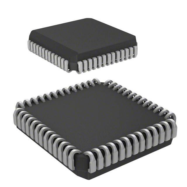
Available in 52-pin plastic leaded chip carrier (PLCC), 52-pin
plastic quad flat package (PQFP)
■
Pb-free packages available
CY7C131E/CY7C131AE/CY7C136E/CY7C136AE
are
high-speed, low-power CMOS 1K/2K × 8 dual-port static RAMs.
Two ports are provided permitting independent access to any
location in memory. The CY7C131E/CY7C131AE/CY7C136E/
CY7C136AE can be used as a standalone dual-port static RAM.
It is the solution to applications requiring shared or buffered data,
such as cache memory for DSP, bit-slice, or multiprocessor
designs.
Each port has independent control pins; chip enable (CE), write
enable (R/W), and output enable (OE). Two flags are provided
on each port, BUSY and INT. The BUSY flag signals that the port
is trying to access the same location, which is currently being
accessed by the other port. The INT is an interrupt flag indicating
that data is placed in a unique location[1]. The BUSY and INT
flags are push pull outputs. An automatic power-down feature is
controlled independently on each port by the chip enable (CE)
pins.
The CY7C131E/CY7C131AE/CY7C136E/CY7C136AE are
available in 52-pin Pb-free PLCC and 52-pin Pb-free PQFP.
For a complete list of related documentation, click here.
Logic Block Diagram
R/WL
CEL
R/WR
CER
OEL
OER
I/O7L
I/O
CONTROL
I/O0L
[2]
BUSYL
I/O
CONTROL
I/O7R
I/O0R
[2]
BUSYR
A 9/10L
[4]
A 0L
ADDR
DECODER
CEL
OEL
MEMORY
ARRAY
ADDR
DECODER
7C131E/7C131AE/
ARBITRATION
7C136E/7C136AE
LOGIC
ARBITRATION
(7C130/7C131 LOGIC
ONLY)
A 9/10R
[4]
A 0R
CER
AND
INTERRUPT LOGIC
OER
INTERRUPT LOGIC
R/WL
R/WR
[3]
INTL
[3]
INTR
Notes
1. Unique location used by interrupt flag: 1K × 8: Left port reads from 3FE, Right port reads from 3FF; 2K × 8: Left port reads from 7FE, Right port reads from 7FF.
2. BUSY is a push-pull output. No pull-up resistor required.
3. INT: push-pull output. No pull-up resistor required.
4. 1K × 8: A0–A9, 2K × 8: A0–A10, address lines are for both left and right ports.
Cypress Semiconductor Corporation
Document Number: 001-64231 Rev. *I
•
198 Champion Court
•
San Jose, CA 95134-1709
•
408-943-2600
Revised November 14, 2017
�CY7C131E/CY7C131AE
CY7C136E/CY7C136AE
Contents
Pin Configurations ........................................................... 3
Pin Definitions .................................................................. 3
Selection Guide ................................................................ 3
Maximum Ratings ............................................................. 4
Operating Range ............................................................... 4
Electrical Characteristics ................................................. 4
Capacitance ...................................................................... 5
AC Test Loads and Waveforms ....................................... 5
Switching Characteristics ................................................ 6
Switching Characteristics ................................................ 8
Switching Waveforms .................................................... 10
Ordering Information ...................................................... 15
Document Number: 001-64231 Rev. *I
Ordering Code Definitions ......................................... 16
Package Diagrams .......................................................... 17
Acronyms ........................................................................ 18
Document Conventions ................................................. 18
Units of Measure ....................................................... 18
Document History Page ................................................. 19
Sales, Solutions, and Legal Information ...................... 21
Worldwide Sales and Design Support ....................... 21
Products .................................................................... 21
PSoC® Solutions ...................................................... 21
Cypress Developer Community ................................. 21
Technical Support ..................................................... 21
Page 2 of 21
�CY7C131E/CY7C131AE
CY7C136E/CY7C136AE
Pin Configurations
Figure 1. 52-pin PLCC pinout (Top View)
I/O5R
I/O6R
A6R
A7R
A8R
A9R
NC
I/O7R
BUSYR
INTR
NC/A10R
CER
R/WR
BUSYL
R/W
L
CEL
VCC
A0L
OEL
NC/A10L
INTL
OER
A0R
A1R
A2R
A3R
A4R
A5R
I/O2R
I/O3R
I/O4R
52 51 50 49 48 47 46 45 44 43 42 41 40
A1L
A2L
A3L
A4L
A5L
A6L
A7L
A8L
A9L
I/O0L
I/O1L
I/O2L
I/O3L
1
2
3
4
5
6
7
8
9
10
11
12
13
OER
A0R
A1R
A2R
A3R
A4R
A5R
39
38
37
36
35
34
33
32
31
30
29
28
27
7C131E/7C131AE
7C136E/7C131AE
A6R
A7R
A8R
A9R
NC
I/O7R
I/O5R
I/O6R
I/O2R
I/O3R
I/O4R
NC
GND
I/O0R
I/O1R
I/O6L
I/O7L
14 15 16 17 18 19 20 21 22 23 24 25 26
I/O4L
I/O5L
I/O0R
I/O1R
NC
GND
I/O6L
I/O7L
7 6 5 4 3 2 1 52 51 50 49 48 47
46
45
44
43
42
41
7C131E/7C131AE
40
7C136E/7C136AE
39
38
37
36
35
34
2122 23 24 25 26 27 28 29 30 31 32 33
[5]
[5]
BUSYR
INTR
NC/A10R
CER
R/WR
BUSYL
R/W
L
CEL
VCC
A0L
OEL
NC/A10L
INTL
8
9
10
11
12
13
14
15
16
17
18
19
20
I/O4L
I/O5L
A1L
A2L
A3L
A4L
A5L
A6L
A7L
A8L
A9L
I/O0L
I/O1L
I/O2L
I/O3L
Figure 2. 52-pin PQFP pinout (Top View)
[5]
[5]
Pin Definitions
Left Port
Right Port
Description
CEL
CER
Chip Enable
R/WL
R/WR
Read/Write Enable
OEL
OER
Output Enable
A0R–A9/10R[5]
Address
I/O0L–I/O7L
I/O0R–I/O7R
Data Bus Input/Output
INTL
INTR
Interrupt Flag
BUSYL
BUSYR
Busy Flag
A0L–A9/10L
[5]
VCC
Power
GND
Ground
Selection Guide
Parameter
7C131E-15
7C131AE-15
7C131E-25
7C136E-25
7C131E-55
7C136E-55
7C136AE-55
Unit
Maximum Access Time
15
25
55
ns
Typical Operating Current
110
100
95
mA
Typical Standby Current for ISB1 (both ports TTL level)
Typical Standby Current for ISB3 (Both ports CMOS level)
50
45
45
mA
0.05
0.05
0.05
mA
Note
5. 1K × 8: A0–A9, 2K × 8: A0–A10, address lines are for both left and right ports.
Document Number: 001-64231 Rev. *I
Page 3 of 21
�CY7C131E/CY7C131AE
CY7C136E/CY7C136AE
DC input voltage [7] ......................................–0.5 V to +7.0 V
Maximum Ratings
Exceeding maximum ratings [6] may shorten the useful life of the
device. User guidelines are not tested.
Output current into outputs (LOW) ............................. 20 mA
Static discharge voltage .......................................... >1100 V
Storage temperature ................................ –65 C to +150 C
Latch up current ..................................................... >200 mA
Ambient temperature
with power applied ................................... –55 C to +125 C
Operating Range
Supply voltage to ground potential ..............–0.3 V to +7.0 V
DC voltage applied to outputs
in High Z State .............................................–0.5 V to +7.0 V
Range
Ambient Temperature
VCC
0C to +70 C
5 V ± 10%
–40 C to +85 C
5 V ± 10%
Commercial
Industrial
Electrical Characteristics
Over the Operating Range
Parameter
Description
Test Conditions
7C131E-15
7C131AE-15
7C131E-25
7C136E-25
7C131E-55
7C136E-55
7C136AE-55
Unit
Min Typ [8] Max Min Typ [8] Max Min Typ [8] Max
VOH
Output HIGH
Voltage
VCC = Min, IOH = –4.0 mA
2.4
–
–
2.4
–
–
2.4
–
–
V
VOL
Output LOW
Voltage
VCC = Min, IOL = 4.0 mA
–
–
0.4
–
–
0.4
–
–
0.4
V
VIH
Input HIGH
Voltage
2.2
–
–
2.2
–
–
2.2
–
–
V
VIL
Input LOW
Voltage
–
–
0.8
–
–
0.8
–
–
0.8
V
IOZ
Output
Leakage
Current
–20
–
+20 –20
–
+20 –20
–
+20
A
ICC
VCC Operating VCC = Max, IOUT = 0 mA
Supply Current Outputs disabled
Commercial
Industrial
–
110
115
190
200
–
100
110
170
180
–
95
105
160
170
mA
ISB1
Standby
Current,
Both Ports,
TTL Inputs
CEL and CER > VIH,
f = fMAX[9]
Commercial
Industrial
–
50
65
70
95
–
45
65
65
95
–
45
65
65
95
mA
ISB2
Standby
Current,
One Port,
TTL Inputs
CEL or CER > VIH,
Active Port Outputs Open,
f = fMAX[9]
Commercial
Industrial
–
120
135
180
205
–
110
135
160
205
–
110
135
160
205
mA
ISB3
Standby
Current,
Both Ports,
CMOS Inputs
Both Ports
Commercial
CEL and CER > VCC – 0.2 V, Industrial
VIN > VCC – 0.2 V
or VIN < 0.2 V, f = 0
–
0.05
0.05
0.5
0.5
–
0.05
0.05
0.5
0.5
–
0.05
0.05
0.5
0.5
mA
ISB4
Standby
Current,
One Port,
CMOS Inputs
One Port
CEL or CER > VCC – 0.2 V,
VIN > VCC – 0.2 V
or VIN < 0.2 V,
Active Port Outputs Open,
f = fMAX[9]
–
110
125
160
175
–
100
125
140
175
–
100
125
140
175
mA
GND < VO < VCC, Output disabled
Commercial
Industrial
Notes
6. The voltage on any I/O pin cannot exceed the power pin during power-up.
7. Pulse width < 20 ns.
8. Typical values are included for reference only and are not guaranteed or tested. Typical values are measured at VCC = VCC(typ.), TA = 25 °C.
9. At f = fMAX, address and data inputs are cycling at the maximum frequency of read cycle of 1/tRC and using AC Test Waveforms input levels of GND to 3 V.
Document Number: 001-64231 Rev. *I
Page 4 of 21
�CY7C131E/CY7C131AE
CY7C136E/CY7C136AE
Capacitance
Parameter [10]
Description
CIN
Input capacitance
COUT
Output capacitance
Test Conditions
TA = 25 C, f = 1 MHz, VCC = 5.0 V
Max
Unit
15
pF
10
pF
AC Test Loads and Waveforms
Figure 3. AC Test Loads and Waveforms
5V
5V
R1 = 893
OUTPUT
C = 30 pF
OUTPUT
R2 = 347
RTH = 250
R1 = 893
OUTPUT
C = 30 pF
C = 5 pF
VTH = 1.4 V
(a) Normal Load (Load 1)
ALL INPUT PULSES
3.0 V
GND
10%
90%
5 ns
(b) Thévenin Equivalent (Load 1)
R2 = 347
(c) Three-State Delay (Load 2)
(Used for tLZ, tHZ, tHZWE, and tLZWE
including scope and jig)
(CY7C131E/CY7C131AE ONLY)
90%
10%
5ns
Note
10. Tested initially and after any design or process changes that may affect these parameters.
Document Number: 001-64231 Rev. *I
Page 5 of 21
�CY7C131E/CY7C131AE
CY7C136E/CY7C136AE
Switching Characteristics
Over the Operating Range
Parameter [11]
Description
7C131E-15/7C131AE-15
7C131E-25/7C136E-25
Unit
Min
Max
Min
Max
15
–
25
–
ns
–
15
–
25
ns
Read Cycle
tRC
Read cycle time
[12]
tAA
Address to data valid
tOHA
Data hold from Address change
3
–
3
–
ns
tACE
CE LOW to data valid
[12]
–
15
–
25
ns
tDOE
OE LOW to data valid [12]
–
10
–
15
ns
3
–
3
–
ns
–
10
–
15
ns
3
–
5
–
ns
–
10
–
15
ns
0
–
0
–
ns
–
15
–
25
ns
tLZOE
tHZOE
OE LOW to Low Z
[13, 14, 15]
OE HIGH to High Z
[13, 14, 15]
[13, 14, 15]
tLZCE
CE LOW to Low Z
tHZCE
CE HIGH to High Z [13, 14, 15]
tPU
tPD
Write Cycle
CE LOW to power-up
[13]
CE HIGH to power-down
[13]
[16]
tWC
Write cycle time
15
–
25
–
ns
tSCE
CE LOW to write end
12
–
20
–
ns
tAW
Address setup to write end
12
–
20
–
ns
tHA
Address hold from write end
0
–
0
–
ns
tSA
Address setup to write start
0
–
0
–
ns
tPWE
R/W pulse width
10
–
12
–
ns
tSD
Data setup to write end
10
–
15
–
ns
tHD
Data hold from write end
0
–
0
–
ns
tHZWE[13]
R/W LOW to High Z [15]
–
10
–
15
ns
tLZWE[13]
[15]
3
–
3
–
ns
R/W HIGH to Low Z
Notes
11. Test conditions assume signal transition times of 5 ns or less, timing reference levels of 1.5 V, input pulse levels of 0 to 3.0 V and output loading of the specified
IOL/IOH, and 30 pF load capacitance.
12. AC Test Conditions use VOH = 1.6 V and VOL = 1.4 V.
13. This parameter is guaranteed but not tested.
14. At any given temperature and voltage condition for any given device, tHZCE is less than tLZCE and tHZOE is less than tLZOE.
15. Parameters tLZCE, tLZWE, tHZOE, tLZOE, tHZCE and tHZWE are tested with CL = 5 pF as in part (c) of Figure 3 on page 5. Transition is measured ±500 mV from steady
state voltage.
16. The internal write time of the memory is defined by the overlap of CE LOW and R/W LOW. Both signals must be low to initiate a write and either signal can terminate
a write by going high. The data input setup and hold timing should be referenced to the rising edge of the signal that terminates the write.
Document Number: 001-64231 Rev. *I
Page 6 of 21
�CY7C131E/CY7C131AE
CY7C136E/CY7C136AE
Switching Characteristics (continued)
Over the Operating Range
Parameter [11]
7C131E-15/7C131AE-15
Description
7C131E-25/7C136E-25
Unit
Min
Max
Min
Max
–
15
–
20
ns
–
15
–
20
ns
Busy/Interrupt Timing[17]
tBLA
BUSY LOW from Address match
[18]
tBHA
BUSY HIGH from Address mismatch
tBLC
BUSY LOW from CE LOW
–
15
–
20
ns
tBHC
BUSY HIGH from CE HIGH [18]
–
15
–
20
ns
tPS
Port setup for priority
5
–
5
–
ns
tBDD
BUSY HIGH to valid data
–
15
–
25
ns
–
25
–
30
ns
–
30
–
45
ns
tDDD
Write data valid to read data valid
tWDD
Write pulse to data delay [19]
[19]
Interrupt Timing
tWINS
R/W to INTERRUPT set time
–
15
–
25
ns
tEINS
CE to INTERRUPT set time
–
15
–
25
ns
tINS
Address to INTERRUPT set time
–
15
–
25
ns
OE to INTERRUPT reset time
[18]
–
15
–
25
ns
CE to INTERRUPT reset time
[18]
–
15
–
25
ns
–
15
–
25
ns
tOINR
tEINR
tINR
Address to
INTERRUPT reset time [18]
Notes
17. Test conditions used are Load 2.
18. These parameters are measured from the input signal changing, until the output pin goes to a high impedance state.
19. A write operation on Port A, where Port A has priority, leaves the data on Port B’s outputs undisturbed until one access time after one of the following:
BUSY on Port B goes HIGH.
Port B’s address toggled.
CE for Port B is toggled.
Document Number: 001-64231 Rev. *I
Page 7 of 21
�CY7C131E/CY7C131AE
CY7C136E/CY7C136AE
Switching Characteristics
Over the Operating Range
Parameter
Description
7C131E-55/7C136E-55/
7C136AE-55
Min
Unit
Max
Read Cycle
tRC
Read cycle time
55
–
ns
tAA
Address to data valid [20]
–
55
ns
tOHA
Data hold from Address change
3
–
ns
CE LOW to data valid
[20]
–
55
ns
tDOE
OE LOW to data valid
[20]
–
25
ns
tLZOE
OE LOW to Low Z [20, 21, 22]
3
–
ns
–
25
ns
5
–
ns
–
25
ns
0
–
ns
–
35
ns
tACE
tHZOE
tLZCE
OE HIGH to High Z
CE LOW to Low Z
[20, 21, 22]
[20, 21, 22]
[20, 21, 22]
tHZCE
CE HIGH to High Z
tPU
CE LOW to power-up [21]
tPD
CE HIGH to power-down
[21]
Write Cycle
tWC
Write cycle time
55
–
ns
tSCE
CE LOW to write end
40
–
ns
tAW
Address setup to write end
40
–
ns
tHA
Address hold from write end
2
–
ns
tSA
Address setup to write start
0
–
ns
tPWE
R/W pulse width
30
–
ns
tSD
Data setup to write end
20
–
ns
tHD
Data hold from write end
0
–
ns
tHZWE
R/W LOW to High Z
[23]
–
25
ns
tLZWE
R/W HIGH to Low Z [23]
3
–
ns
Notes
20. The internal write time of the memory is defined by the overlap of CE LOW and R/W LOW. Both signals must be low to initiate a write and either signal can terminate
a write by going high. The data input setup and hold timing should be referenced to the rising edge of the signal that terminates the write.
21. AC Test Conditions use VOH = 1.6 V and VOL = 1.4 V.
22. These parameters are measured from the input signal changing, until the output pin goes to a high impedance state.
23. Parameters tLZCE, tLZWE, tHZOE, tLZOE, tHZCE and tHZWE are tested with C = 5 pF as in part (b) of Figure 3 on page 5. Transition is measured ±500 mV from steady
state voltage.
Document Number: 001-64231 Rev. *I
Page 8 of 21
�CY7C131E/CY7C131AE
CY7C136E/CY7C136AE
Switching Characteristics (continued)
Over the Operating Range
Parameter
Description
7C131E-55/7C136E-55/
7C136AE-55
Unit
Min
Max
–
30
ns
–
30
ns
–
30
ns
–
30
ns
5
–
ns
–
45
ns
–
30
ns
–
45
ns
Busy/Interrupt Timing [24]
tBLA
BUSY LOW from Address match
tBHA
BUSY HIGH from Address mismatch
tBLC
BUSY LOW from CE LOW
tBHC
BUSY HIGH from CE HIGH
tPS
Port setup for priority
tBDD
BUSY HIGH to valid data
tDDD
tWDD
[25]
Write data valid to read data valid
Write pulse to data delay
[25]
[25]
[25]
Interrupt Timing
tWINS
R/W to INTERRUPT set time
–
45
ns
tEINS
CE to INTERRUPT set time
–
45
ns
tINS
Address to INTERRUPT set time
–
45
ns
tOINR
OE to INTERRUPT reset time [26]
–
45
ns
tEINR
[26]
–
45
ns
–
45
ns
tINR
CE to INTERRUPT reset time
Address to
INTERRUPT reset time [26]
Notes
24. Test conditions used are Load 2.
25. A write operation on Port A, where Port A has priority, leaves the data on Port B’s outputs undisturbed until one access time after one of the following:
BUSY on Port B goes HIGH.
Port B’s address toggled.
CE for Port B is toggled.
R/W for Port B is toggled during valid read.
26. These parameters are measured from the input signal changing, until the output pin goes to a high impedance state.
Document Number: 001-64231 Rev. *I
Page 9 of 21
�CY7C131E/CY7C131AE
CY7C136E/CY7C136AE
Switching Waveforms
Figure 4. Read Cycle No. 1 [27, 28]
Either Port ADDR Access
tRC
ADDR
tAA
tOHA
DATA OUT
PREVIOUS DATAVALID
DATA VALID
Figure 5. Read Cycle No. 2 [27, 29]
Either Port CE/OE Access
CE
tHZCE
tACE
OE
tLZOE
tHZOE
tDOE
tLZCE
DATA VALID
DATA OUT
tPU
tPD
ICC
ISB
Figure 6. Write Cycle No. 1 (OE Three-States Data I/Os – Either Port) [30, 31]
Either Port
tWC
ADDR
tSCE
CE
tSA
tAW
tPWE
tHA
R/W
tSD
DATAIN
tHD
DATA VALID
OE
tHZOE
DOUT
HIGH IMPEDANCE
Notes
27. R/W is HIGH for read cycle.
28. Device is continuously selected, CE = VIL and OE = VIL.
29. Address valid prior to or coincident with CE transition LOW.
30. The internal write time of the memory is defined by the overlap of CE LOW and R/W LOW. Both signals must be LOW to initiate a write and either signal can
terminate a write by going HIGH. The data input setup and hold timing must be referenced to the rising edge of the signal that terminates the write.
31. If OE is LOW during a R/W controlled write cycle, the write pulse width must be the larger of tPWE or tHZWE + tSD to allow the data I/O pins to enter high impedance
and for data to be placed on the bus for the required tSD.
Document Number: 001-64231 Rev. *I
Page 10 of 21
�CY7C131E/CY7C131AE
CY7C136E/CY7C136AE
Switching Waveforms (continued)
Figure 7. Write Cycle No. 2 (R/W Three-States Data I/Os – Either Port) [32, 33]
tWC
ADDR
tSCE
tHA
CE
tAW
tSA
tPWE[34]
R/W
tSD
DATAIN
tHD
DATA VALID
tLZWE
[35]
tHZWE
HIGH IMPEDANCE
DATAOUT
Figure 8. Read Cycle No. 3 [36]
Read with BUSY
tRC
ADDR R
ADDR MATCH
tPWE
R/WR
tHD
DINR
VALID
ADDR MATCH
ADDR L
tPS
tBHA
BUSYL
tBLA
tBDD
DOUTL
VALID
tWDD
tDDD
Notes
32. These parameters are measured from the input signal changing, until the output pin goes to a high impedance state.
33. If the CE LOW transition occurs simultaneously with or after the R/W LOW transition, the outputs remain in a high impedance state.
34. If OE is LOW during a R/W controlled write cycle, the write pulse width must be the larger of tPWE or (tHZWE + tSD) to allow the I/O drivers to turn off and
data to be placed on the bus for the required tSD. If OE is HIGH during a R/Wn controlled write cycle, this requirements does not apply and the write pulse can
be as short as the specified tPWE.
35. Transition is measured ±500 mV from steady state with a 5 pF load (including scope and jig). This parameter is sampled and not 100% tested.
36. CEL = CER = LOW.
Document Number: 001-64231 Rev. *I
Page 11 of 21
�CY7C131E/CY7C131AE
CY7C136E/CY7C136AE
Switching Waveforms (continued)
Figure 9. Busy Timing Diagram No. 1 (CE Arbitration) [37]
CEL Valid First:
ADDR L,R
ADDR MATCH
CEL
tPS
CER
tBLC
tBHC
BUSYR
CER Valid First:
ADDRL,R
ADDR MATCH
CER
tPS
CEL
tBLC
tBHC
BUSYL
Figure 10. Busy Timing Diagram No. 2 (ADDR Arbitration) [37]
Left ADDR Valid First:
ADDRL
tRC or tWC
ADDR MATCH
ADDR MISMATCH
tPS
ADDR R
tBLA
tBHA
BUSYR
Right Address Valid First:
tRC or tWC
ADDRR
ADDR MATCH
ADDR MISMATCH
tPS
ADDRL
tBLA
tBHA
BUSYL
Note
37. If tPS is violated, the busy signal will be asserted on one side or the other, but there is no guarantee to which side BUSY will be asserted.
Document Number: 001-64231 Rev. *I
Page 12 of 21
�CY7C131E/CY7C131AE
CY7C136E/CY7C136AE
Switching Waveforms (continued)
Figure 11. Interrupt Timing Diagrams
Left Side Sets INTR
tWC
ADDR L
WRITE 3FF/7FF
[39]
tINS[38]
tHA
CEL
tEINS
R/WL
tSA
tWINS
INTR
Right Side Clears INTR
tRC
ADDRR
READ 3FF/7FF
[39]
tHA
[38]
tINR
CER
tEINR
R/WR
OER
tOINR
INTR
Notes
38. Parameter tINS or tINR depends on which enable pin (CEL or R/WL) is asserted last.
39. Parameter tHA depends on which enable pin (CEL or R/WL) is deasserted first.
Document Number: 001-64231 Rev. *I
Page 13 of 21
�CY7C131E/CY7C131AE
CY7C136E/CY7C136AE
Switching Waveforms (continued)
Figure 12. Interrupt Timing Diagrams
Right Side Sets INTL
t WC
ADDRR
WRITE 3FE/7FE
[40]
tHA[41]
tINS
CER
tEINS
R/WR
INTL
tSA
tWINS
Left Side Clears INTL
tRC
ADDR R
READ 3FE/7FE
[41]
tHA
CEL
[40]
tINR
tEINR
R/WL
OEL
tOINR
INTL
Notes
40. Parameter tINS or tINR depends on which enable pin (CEL or R/WL) is asserted last.
41. Parameter tHA depends on which enable pin (CEL or R/WL) is deasserted first.
Document Number: 001-64231 Rev. *I
Page 14 of 21
�CY7C131E/CY7C131AE
CY7C136E/CY7C136AE
Ordering Information
Speed
(ns)
Ordering Code
Package
Name
Package Type
Operating
Range
1K × 8 Dual-port SRAM
15
25
55
CY7C131E-15NXI
51-85042 52-pin PQFP (Pb-free)
CY7C131E-15NXIT
51-85042 52-pin PQFP (Pb-free), Tape and Reel
CY7C131E-25JXC
51-85004 52-pin PLCC (Pb-free)
CY7C131E-25JXCT
51-85004 52-pin PLCC (Pb-free), Tape and Reel
CY7C131E-25NXC
51-85042 52-pin PQFP (Pb-free)
CY7C131E-25NXCT
51-85042 52-pin PQFP (Pb-free), Tape and Reel
CY7C131E-55JXC
51-85004 52-pin PLCC (Pb-free)
CY7C131E-55JXCT
51-85004 52-pin PLCC (Pb-free), Tape and Reel
CY7C131E-55NXC
51-85042 52-pin PQFP (Pb-free)
CY7C131E-55NXCT
51-85042 52-pin PQFP (Pb-free), Tape and Reel
CY7C131E-55JXI
51-85004 52-pin PLCC (Pb-free)
CY7C131E-55JXIT
51-85004 52-pin PLCC (Pb-free), Tape and Reel
Industrial
Commercial
Commercial
Industrial
2K × 8 Dual-port SRAM
25
55
CY7C136E-25JXC
51-85004 52-pin PLCC (Pb-free)
CY7C136E-25JXCT
51-85004 52-pin PLCC (Pb-free), Tape and Reel
CY7C136E-25NXC
51-85042 52-pin PQFP (Pb-free)
CY7C136E-25NXCT
51-85042 52-pin PQFP (Pb-free), Tape and Reel
CY7C136E-25JXI
51-85004 52-pin PLCC (Pb-free)
CY7C136E-25JXIT
51-85004 52-pin PLCC (Pb-free), Tape and Reel
CY7C136E-55JXC
51-85004 52-pin PLCC (Pb-free)
CY7C136E-55JXCT
51-85004 52-pin PLCC (Pb-free), Tape and Reel
CY7C136E-55NXC
51-85042 52-pin PQFP (Pb-free)
CY7C136E-55NXCT
51-85042 52-pin PQFP (Pb-free), Tape and Reel
CY7C136AE-55JXI
51-85004 52-pin PLCC (Pb-free)
CY7C136AE-55JXIT
51-85004 52-pin PLCC (Pb-free), Tape and Reel
CY7C136AE-55NXI
51-85042 52-pin PQFP (Pb-free)
CY7C136AE-55NXIT
51-85042 52-pin PQFP (Pb-free), Tape and Reel
Document Number: 001-64231 Rev. *I
Commercial
Industrial
Commercial
Industrial
Page 15 of 21
�CY7C131E/CY7C131AE
CY7C136E/CY7C136AE
Ordering Code Definitions
CY 7
C 13X X
E - XX X
X
X
X
X = blank or T
blank = Tube; T = Tape and Reel
Temperature Grade: X = I or C
I = Industrial; C = Commercial
Pb-free
Package Type: X = J or N
J = 52-pin PLCC; N = 52-pin PQFP
Speed Grade: XX = 15 or 25 or 55
15 = 15 ns; 25 = 25 ns; 55 = 55 ns
Process Version
X = A or blank
Part Identifier: 13X = 131 or 136
Technology Code: C = CMOS
Marketing Code: 7 = SRAM
Company ID: CY = Cypress
Document Number: 001-64231 Rev. *I
Page 16 of 21
�CY7C131E/CY7C131AE
CY7C136E/CY7C136AE
Package Diagrams
Figure 13. 52-pin PLCC (0.756 × 0.756 Inches) J52 Package Outline, 51-85004
51-85004 *D
Figure 14. 52-pin PQFP (10 × 10 × 2.0 mm) N5210 Package Outline, 51-85042
51-85042 *E
Document Number: 001-64231 Rev. *I
Page 17 of 21
�CY7C131E/CY7C131AE
CY7C136E/CY7C136AE
Acronyms
Acronym
Document Conventions
Description
Units of Measure
CE
Chip Enable
CMOS
Complementary Metal Oxide Semiconductor
°C
degree Celsius
I/O
Input/Output
µA
microampere
OE
Output Enable
mA
milliampere
PLCC
Plastic Leaded Chip Carrier
mV
millivolt
PQFP
Plastic Quad Flat Package
ns
nanosecond
SRAM
Static Random Access Memory
ohm
TTL
Transistor-Transistor Logic
%
percent
WE
Write Enable
pF
picofarad
V
volt
W
watt
Document Number: 001-64231 Rev. *I
Symbol
Unit of Measure
Page 18 of 21
�CY7C131E/CY7C131AE
CY7C136E/CY7C136AE
Document History Page
Document Title: CY7C131E/CY7C131AE/CY7C136E/CY7C136AE, 1K/2K × 8 Dual-Port Static RAM
Document Number: 001-64231
Rev.
ECN No.
Orig. of
Change
Submission
Date
**
3038037
ADMU
09/24/2010
New data sheet.
*A
3394800
ADMU
10/04/2011
Changed status from Preliminary to Final.
Updated Maximum Ratings (Removed (Pin 48 to Pin 24)).
Updated Electrical Characteristics (changed minimum value of IOZ parameter
from –10 µA to –20 µA, changed maximum value of IOZ parameter from +10 µA
to +20 µA and changed maximum value of ISB3 from 0.5 mA to 15 mA for both
Commercial and Industrial temperature ranges).
Updated Package Diagrams (Updated revision of 51-85004 from *B to *C and
revision of 51-85042 from *A to *C).
Updated in new template.
*B
3403147
ADMU
10/12/2011
No technical updates.
*C
3435230
ADMU
11/17/2011
Updated Features (Removed a feature “Expandable data bus width to 16 bits
or more using Master/Slave chip select when using more than one device.” and
updated another feature to read as “BUSY output flag to indicate access to the
same location by both ports.”.
Updated Functional Description (Updated the sentence in the first paragraph
to read as “The CY7C131E / CY7C131AE / CY7C136E / CY7C136AE can be
used as a standalone dual-port static RAM.”.
Updated Note 2 to read as “BUSY is a push-pull output. No pull-up resistor
required.”.
Updated Note 3 to read as “Interrupt: push-pull output. No pull-up resistor
required.”.
Updated Maximum Ratings (Removed “(per MIL-STD-883, Method 3015)”).
Updated Electrical Characteristics (Removed the Note “See the last page of
this specification for Group A subgroup testing information.” and its reference
in Parameter column.).
Updated Capacitance (Changed maximum value of CIN parameter from 10 pF to
15 pF).
Updated AC Test Loads and Waveforms.
Updated Switching Characteristics (Removed the Note “See the last page of
this specification for Group A subgroup testing information.” and its reference
in Parameter column.).
Updated Switching Characteristics (Changed the minimum value of tOHA from
0 ns to 3 ns).
Removed the section “Typical DC and AC Characteristics”.
Removed the section “Reference Documents”.
Document Number: 001-64231 Rev. *I
Description of Change
Page 19 of 21
�CY7C131E/CY7C131AE
CY7C136E/CY7C136AE
Document History Page (continued)
Document Title: CY7C131E/CY7C131AE/CY7C136E/CY7C136AE, 1K/2K × 8 Dual-Port Static RAM
Document Number: 001-64231
Rev.
ECN No.
Orig. of
Change
Submission
Date
*D
3620277
ADMU
06/15/2012
Updated missing overbars in all instances across the document.
Updated Selection Guide:
Updated all values of “Typical Operating Current” parameter.
Updated Maximum Ratings:
Changed value of “Static discharge voltage” from “>2001 V” to “>1100 V”.
Updated Electrical Characteristics:
Fixed typos.
Added Note 8 and referred the same note in “Typ” column.
Updated all values of ICC parameter.
Updated AC Test Loads and Waveforms:
Updated Figure 3 (Replaced 3 ns with 5 ns).
Updated Switching Characteristics:
Added Note 17 and referred the same note in “Busy/Interrupt Timing”.
Updated Switching Characteristics:
Added Note 24 and referred the same note in “Busy/Interrupt Timing”.
Updated Switching Waveforms:
Added Note 34 and referred the same note in “tPWE” in Figure 7.
Added Note 35 and referred the same note in “tPWE” in Figure 7.
Added Note 38 and referred the same note in “tINS” in Figure 11.
Added Note 39 and referred the same note in “tHA” in Figure 11.
Added Note 40 and referred the same note in “tINS” in Figure 12.
Added Note 41 and referred the same note in “tHA” in Figure 12.
Removed “Busy Timing Diagram No. 3”.
Updated Package Diagrams:
spec 51-85042 – Changed revision from *C to *D.
*E
3997575
ADMU
05/15/2013
Updated Package Diagrams:
spec 51-85004 – Changed revision from *C to *D.
Added
Appendix: Silicon Errata for CY7C131E/131AE/136E/136AE 1K/2K × 8
Dual Port Static RAM.
*F
4241174
ADMU
01/09/2014
Removed
Appendix: Silicon Errata for CY7C131E/131AE/136E/136AE 1K/2K × 8
Dual Port Static RAM.
Updated to new template.
*G
4559526
AMDU
11/07/2014
Updated Functional Description:
Added “For a complete list of related documentation, click here.” at the end.
*H
5397125
NILE
08/09/2016
Updated Ordering Information:
Updated part numbers.
Updated Package Diagrams:
spec 51-85042 – Changed revision from *D to *E.
Updated to new template.
*I
5966445
AESATMP8
11/14/2017
Updated logo and Copyright.
Document Number: 001-64231 Rev. *I
Description of Change
Page 20 of 21
�CY7C131E/CY7C131AE
CY7C136E/CY7C136AE
Sales, Solutions, and Legal Information
Worldwide Sales and Design Support
Cypress maintains a worldwide network of offices, solution centers, manufacturer’s representatives, and distributors. To find the office
closest to you, visit us at Cypress Locations.
PSoC® Solutions
Products
ARM® Cortex® Microcontrollers
Automotive
cypress.com/arm
cypress.com/automotive
Clocks & Buffers
Interface
Internet of Things
Memory
cypress.com/clocks
cypress.com/interface
cypress.com/iot
cypress.com/memory
Microcontrollers
cypress.com/mcu
PSoC
cypress.com/psoc
Power Management ICs
Touch Sensing
USB Controllers
Wireless Connectivity
PSoC 1 | PSoC 3 | PSoC 4 | PSoC 5LP | PSoC 6
Cypress Developer Community
Forums | WICED IOT Forums | Projects | Video | Blogs |
Training | Components
Technical Support
cypress.com/support
cypress.com/pmic
cypress.com/touch
cypress.com/usb
cypress.com/wireless
© Cypress Semiconductor Corporation, 2010-2017. This document is the property of Cypress Semiconductor Corporation and its subsidiaries, including Spansion LLC (“Cypress”). This document,
including any software or firmware included or referenced in this document (“Software”), is owned by Cypress under the intellectual property laws and treaties of the United States and other countries
worldwide. Cypress reserves all rights under such laws and treaties and does not, except as specifically stated in this paragraph, grant any license under its patents, copyrights, trademarks, or other
intellectual property rights. If the Software is not accompanied by a license agreement and you do not otherwise have a written agreement with Cypress governing the use of the Software, then Cypress
hereby grants you a personal, non-exclusive, nontransferable license (without the right to sublicense) (1) under its copyright rights in the Software (a) for Software provided in source code form, to
modify and reproduce the Software solely for use with Cypress hardware products, only internally within your organization, and (b) to distribute the Software in binary code form externally to end users
(either directly or indirectly through resellers and distributors), solely for use on Cypress hardware product units, and (2) under those claims of Cypress's patents that are infringed by the Software (as
provided by Cypress, unmodified) to make, use, distribute, and import the Software solely for use with Cypress hardware products. Any other use, reproduction, modification, translation, or compilation
of the Software is prohibited.
TO THE EXTENT PERMITTED BY APPLICABLE LAW, CYPRESS MAKES NO WARRANTY OF ANY KIND, EXPRESS OR IMPLIED, WITH REGARD TO THIS DOCUMENT OR ANY SOFTWARE
OR ACCOMPANYING HARDWARE, INCLUDING, BUT NOT LIMITED TO, THE IMPLIED WARRANTIES OF MERCHANTABILITY AND FITNESS FOR A PARTICULAR PURPOSE. To the extent
permitted by applicable law, Cypress reserves the right to make changes to this document without further notice. Cypress does not assume any liability arising out of the application or use of any
product or circuit described in this document. Any information provided in this document, including any sample design information or programming code, is provided only for reference purposes. It is
the responsibility of the user of this document to properly design, program, and test the functionality and safety of any application made of this information and any resulting product. Cypress products
are not designed, intended, or authorized for use as critical components in systems designed or intended for the operation of weapons, weapons systems, nuclear installations, life-support devices or
systems, other medical devices or systems (including resuscitation equipment and surgical implants), pollution control or hazardous substances management, or other uses where the failure of the
device or system could cause personal injury, death, or property damage (“Unintended Uses”). A critical component is any component of a device or system whose failure to perform can be reasonably
expected to cause the failure of the device or system, or to affect its safety or effectiveness. Cypress is not liable, in whole or in part, and you shall and hereby do release Cypress from any claim,
damage, or other liability arising from or related to all Unintended Uses of Cypress products. You shall indemnify and hold Cypress harmless from and against all claims, costs, damages, and other
liabilities, including claims for personal injury or death, arising from or related to any Unintended Uses of Cypress products.
Cypress, the Cypress logo, Spansion, the Spansion logo, and combinations thereof, WICED, PSoC, CapSense, EZ-USB, F-RAM, and Traveo are trademarks or registered trademarks of Cypress in
the United States and other countries. For a more complete list of Cypress trademarks, visit cypress.com. Other names and brands may be claimed as property of their respective owners.
Document Number: 001-64231 Rev. *I
Revised November 14, 2017
Page 21 of 21
�