CY7C1370B
CY7C1372B
512K × 36/1M × 18 Pipelined SRAM with NoBL Architecture
Features
• Zero Bus Latency, no dead cycles between Write and
Read cycles
• Fast clock speed: 200, 167, 150, and 133 MHz
• Fast access time: 3.0, 3.4, 3.8, and 4.2 ns
• Internally synchronized registered outputs eliminate
the need to control OE
• Single 3.3V –5% and +10% power supply VDD
• Separate VDDQ for 3.3V or 2.5V I/O
• Single WE (Read/Write) control pin
• Positive clock-edge triggered address, data, and
control signal registers for fully pipelined applications
• Interleaved or linear four-word burst capability
• Individual byte Write (BWSa–BWSd) control (may be
tied LOW)
• CEN pin to enable clock and suspend operations
• Three chip enables for simple depth expansion
• JTAG boundary scan (BGA package only)
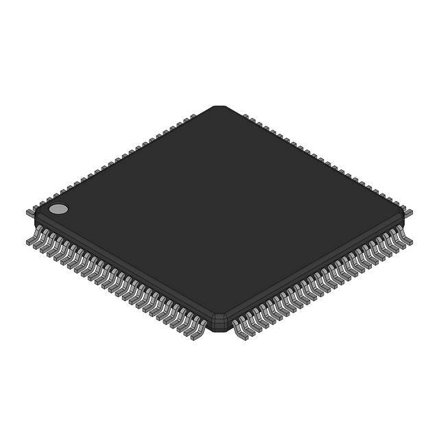
• Available in 119-ball bump BGA and 100-pin TQFP
packages
• Automatic power down available using ZZ mode or CE
deselect
Functional Description
The CY7C1370B and CY7C1372B SRAMs are designed to
eliminate dead cycles when transitions from Read to Write or
vice versa. These SRAMs are optimized for 100 percent bus
utilization and achieve Zero Bus Latency™. They integrate
524,288 × 36 and 1,048,576 × 18 SRAM cells, respectively,
with advanced synchronous peripheral circuitry and a 2-bit
counter for internal burst operation. The Synchronous Burst
SRAM family employs high-speed, low-power CMOS designs
using advanced single-layer polysilicon, three-layer metal
technology. Each memory cell consists of six transistors.
All synchronous inputs are gated by registers controlled by a
positive-edge-triggered Clock input (CLK). The synchronous
inputs include all addresses, all data inputs, depth-expansion
Chip Enables (CE1, CE2, and CE3), cycle start input (ADV/LD),
Clock enable (CEN), byte Write Enables (BWSa, BWSb,
BWSc, and BWSd), and Read-Write Control (WE). BWSc and
BWSd apply to CY7C1370B only.
Address and control signals are applied to the SRAM during
one clock cycle, and two cycles later, its associated data
occurs, either Read or Write.
A Clock enable (CEN) pin allows operation of the
CY7C1370B/CY7C1372B to be suspended as long as
necessary. All synchronous inputs are ignored when CEN is
HIGH and the internal device registers will hold their previous
values.
There are three chip enable pins (CE1, CE2, CE3) that allow
the user to deselect the device when desired. If any one of
these three are not active when ADV/LD is LOW, no new
memory operation can be initiated and any burst cycle in
progress is stopped. However, any pending data transfers
(Read or Write) will be completed. The data bus will be in
high-impedance state two cycles after the chip is deselected
or a Write cycle is initiated.
The CY7C1370B and CY7C1372B have an on-chip two-bit
burst counter. In the burst mode, the CY7C1370B and
CY7C1372B provide four cycles of data for a single address
presented to the SRAM. The order of the burst sequence is
defined by the MODE input pin. The MODE pin selects
between linear and interleaved burst sequence. The ADV/LD
signal is used to load a new external address (ADV/LD = LOW)
or increment the internal burst counter (ADV/LD = HIGH)
Output enable (OE) and burst sequence select (MODE) are
the asynchronous signals. OE can be used to disable the
outputs at any given time. ZZ may be tied to LOW if it is not
used.
Four pins are used to implement JTAG test capabilities. The
JTAG circuitry is used to serially shift data to and from the
device. JTAG inputs use LVTTL/LVCMOS levels to shift data
during this testing mode of operation.
Logic Block Diagram
CLK
CE
D
Data-In REG.
Q
Ax
AX
CY7C1370 CY7C1372
X = 18:0
X = 19:0
DQX
X = a, b, c, d X = a, b
DPX
BWSX
X = a, b, c, d X = a, b
X = a, b, c, d X = a, b
CEN
CE1
CE2
CE3
WE
BWSX
CONTROL
and Write
LOGIC
256K × 36/
512K × 18
MEMORY
ARRAY
OUTOUT
REGISTERS
and LOGIC
ADV/LD
DQX
DPX
Mode
OE
Cypress Semiconductor Corporation
Document #: 38-05197 Rev. *C
•
3901 North First Street
•
San Jose, CA 95134
•
408-943-2600
Revised January 18, 2003
�CY7C1370B
CY7C1372B
.
Selection Guide
200 MHz
Maximum Access Time
Maximum Operating Current
Commercial
Maximum CMOS Standby Current
167 MHz
150 MHz
133 MHz
Unit
3.0
3.4
3.8
4.2
ns
315
285
265
245
mA
20
20
20
20
mA
Pin Configurations
CY7C1370B
100
99
98
97
96
95
94
93
92
91
90
89
88
87
86
85
84
83
82
81
DPb
DQb
DQb
VDDQ
VSS
VDDQ
VSS
NC
NC
DQb
DQb
VSS
VDDQ
DQb
DQb
NC
VDD
NC
VSS
DQb
DQb
VDDQ
VSS
DQb
DQb
DPb
NC
VSS
VDDQ
NC
NC
NC
1
2
3
4
5
6
7
8
9
10
11
12
13
14
15
16
17
18
19
20
21
22
23
24
25
26
27
28
29
30
CY7C1372B
(1M × 18)
80
79
78
77
76
75
74
73
72
71
70
69
68
67
66
65
64
63
62
61
60
59
58
57
56
55
54
53
52
51
Document #: 38-05197 Rev. *C
A
NC
NC
VDDQ
VSS
NC
DPa
DQa
DQa
VSS
VDDQ
DQa
DQa
VSS
NC
VDD
ZZ
DQa
DQa
VDDQ
VSS
DQa
DQa
NC
NC
VSS
VDDQ
NC
NC
NC
DNU
DNU
A
A
A
A
A
A
A
DNU
DNU
A
A
A
A
A
A
A
31
32
33
34
35
36
37
38
39
40
41
42
43
44
45
46
47
48
49
50
DQb
DQb
DQb
DQb
VSS
VDDQ
DQb
DQb
VSS
NC
VDD
ZZ
DQa
DQa
VDDQ
VSS
DQa
DQa
DQa
DQa
VSS
VDDQ
DQa
DQa
DPa
NC
NC
NC
MODE
A
A
A
A
A1
A0
DNU
DNU
VSS
VDD
(512K × 36)
80
79
78
77
76
75
74
73
72
71
70
69
68
67
66
65
64
63
62
61
60
59
58
57
56
55
54
53
52
51
31
32
33
34
35
36
37
38
39
40
41
42
43
44
45
46
47
48
49
50
DQc
DQc
NC
VDD
NC
VSS
DQd
DQd
VDDQ
VSS
DQd
DQd
DQd
DQd
VSS
VDDQ
DQd
DQd
DPd
1
2
3
4
5
6
7
8
9
10
11
12
13
14
15
16
17
18
19
20
21
22
23
24
25
26
27
28
29
30
MODE
A
A
A
A
A1
A0
DNU
DNU
VSS
VDD
DPc
DQc
DQc
VDDQ
VSS
DQc
DQc
DQc
DQc
VSS
VDDQ
A
A
A
A
CE1
CE2
NC
NC
BWSb
BWSa
CE3
VDD
VSS
CLK
WE
CEN
OE
ADV/LD
A
A
A
A
100
99
98
97
96
95
94
93
92
91
90
89
88
87
86
85
84
83
82
81
A
A
CE1
CE2
BWSd
BWSc
BWSb
BWSa
CE3
VDD
VSS
CLK
WE
CEN
OE
ADV/LD
A
A
100-Pin TQFP Packages
Page 2 of 27
�CY7C1370B
CY7C1372B
Pin Configurations (continued)
119-ball Bump BGA
CY7C1370B (512K × 36) – 7 × 17 BGA
1
2
3
4
5
6
7
A
VDDQ
A
A
A
A
A
VDDQ
B
C
D
E
F
G
H
J
K
L
M
N
P
NC
NC
CE2
A
A
A
ADV/LD
VDD
A
A
CE3
A
NC
NC
DQc
DPc
VSS
NC
VSS
DPb
DQb
DQc
DQc
VSS
CE1
VSS
DQb
DQb
VDDQ
DQc
VSS
OE
VSS
DQb
VDDQ
R
T
U
DQc
DQc
BWSc
A
BWSb
DQb
DQb
DQc
VDDQ
DQc
VDD
VSS
NC
WE
VDD
VSS
NC
DQb
VDD
DQb
VDDQ
DQd
DQd
DQd
DQd
VSS
BWSd
CLK
NC
VSS
BWSa
DQa
DQa
DQa
DQa
VDDQ
DQd
VSS
CEN
VSS
DQa
VDDQ
DQd
DQd
VSS
A1
VSS
DQa
DQa
DQd
DPd
VSS
A0
VSS
DPa
DQa
NC
A
MODE
VDD
NC
A
NC
NC
64M
A
A
A
32M
ZZ
VDDQ
TMS
TDI
TCK
TDO
NC
VDDQ
CY7C1372B (1M × 18) – 7 × 17 BGA
A
B
C
D
E
F
G
H
J
K
L
M
N
P
R
T
U
Document #: 38-05197 Rev. *C
1
2
3
4
5
6
7
VDDQ
A
A
A
A
A
VDDQ
NC
CE2
A
ADV/LD
A
CE3
NC
NC
A
A
VDD
A
A
NC
DQb
NC
VSS
NC
VSS
DPa
NC
NC
DQb
VSS
CE1
VSS
NC
DQa
VDDQ
NC
VSS
OE
VSS
DQa
VDDQ
NC
DQb
VDDQ
DQb
NC
VDD
BWSb
VSS
NC
A
WE
VDD
VSS
VSS
NC
NC
DQa
VDD
DQa
NC
VDDQ
NC
DQb
VSS
CLK
VSS
NC
DQa
DQb
NC
VSS
NC
BWSa
DQa
NC
VDDQ
DQb
VSS
CEN
VSS
NC
VDDQ
DQb
NC
VSS
A1
VSS
DQa
NC
NC
DPb
VSS
A0
VSS
NC
DQa
NC
NC
A
MODE
VDD
NC
A
64M
A
A
32M
A
A
ZZ
VDDQ
TMS
TDI
TCK
TDO
NC
VDDQ
Page 3 of 27
�CY7C1370B
CY7C1372B
Pin Configurations (continued)
165-ball Bump FBGA
CY7C1370B (512K × 36) – 11 × 15 FBGA
1
2
3
4
5
6
7
8
9
10
11
A
NC
A
CE1
BWSc
BWSb
CE3
CEN
ADV/LD
A
A
NC
B
C
D
E
F
G
H
J
K
L
M
N
P
NC
DPc
A
NC
CE2
VDDQ
BWSd
VSS
BWSa
VSS
CLK
VSS
WE
VSS
OE
VSS
A
VDDQ
A
NC
128M
DPb
DQb
R
DQc
DQc
VDDQ
VDD
VSS
VSS
VSS
VDD
VDDQ
DQb
DQc
DQc
VDDQ
VDD
VSS
VSS
VSS
VDD
VDDQ
DQb
DQb
DQc
DQc
VDDQ
VDD
VSS
VSS
VSS
VDD
VDDQ
DQb
DQb
DQc
DQc
VDDQ
VDD
VSS
VSS
VSS
VDD
VDDQ
DQb
DQb
NC
DQd
VDD
DQd
NC
VDDQ
VDD
VDD
VSS
VSS
VSS
VSS
VSS
VSS
VDD
VDD
NC
VDDQ
NC
DQa
ZZ
DQa
DQd
DQd
DQd
DQd
VDDQ
VDDQ
VDD
VDD
VSS
VSS
VSS
VSS
VSS
VSS
VDD
VDD
VDDQ
VDDQ
DQa
DQa
DQa
DQa
DQd
DQd
VDDQ
VDD
VSS
VSS
VSS
VDD
VDDQ
DQa
DQa
DPd
NC
VDDQ
VSS
NC
NC
NC
VSS
VDDQ
NC
DPa
NC
64M
A
A
TDI
A1
TDO
A
A
A
NC
MODE
32M
A
A
TMS
A0
TCK
A
A
A
A
11
CY7C1372B (1M × 18) – 11 × 15 FBGA
1
2
3
4
5
6
7
8
9
10
A
NC
A
CE1
BWSb
NC
CE3
CEN
ADV/LD
A
A
A
B
C
D
E
F
G
H
J
K
L
M
N
P
NC
NC
A
NC
CE2
VDDQ
NC
VSS
BWSa
VSS
CLK
VSS
WE
VSS
OE
VSS
A
VDDQ
A
NC
128M
DPa
NC
DQb
VDDQ
VDD
VSS
VSS
VSS
VDD
VDDQ
NC
DQa
NC
DQb
VDDQ
VDD
VSS
VSS
VSS
VDD
VDDQ
NC
DQa
NC
DQb
VDDQ
VDD
VSS
VSS
VSS
VDD
VDDQ
NC
DQa
NC
DQb
VDDQ
VDD
VSS
VSS
VSS
VDD
VDDQ
NC
DQa
NC
DQb
VDD
NC
NC
VDDQ
VDD
VDD
VSS
VSS
VSS
VSS
VSS
VSS
VDD
VDD
NC
VDDQ
NC
DQa
ZZ
NC
DQb
DQb
NC
NC
VDDQ
VDDQ
VDD
VDD
VSS
VSS
VSS
VSS
VSS
VSS
VDD
VDD
VDDQ
VDDQ
DQa
DQa
NC
NC
DQb
NC
VDDQ
VDD
VSS
VSS
VSS
VDD
VDDQ
DQa
NC
DPb
NC
VDDQ
VSS
NC
NC
NC
VSS
VDDQ
NC
NC
NC
64M
A
A
TDI
A1
TDO
A
A
A
NC
MODE
32M
A
A
TMS
A0
TCK
A
A
A
A
R
Document #: 38-05197 Rev. *C
Page 4 of 27
�CY7C1370B
CY7C1372B
Pin Definitions
Name
I/O Type
Description
A0
A1
A
InputSynchronous
Address inputs used to select one of the 524,288/1,048576 address locations.
Sampled at the rising edge of the CLK.
BWSa
BWSb
BWSc
BWSd
InputSynchronous
Byte Write Select inputs, active LOW. Qualified with WE to conduct writes to the SRAM.
Sampled on the rising edge of CLK. BWSa controls DQa and DPa, BWSb controls DQb
and DPb, BWSc controls DQc and DPc, BWSd controls DQd and DPd.
WE
InputSynchronous
Write enable input, active LOW. Sampled on the rising edge of CLK if CEN is active
LOW. This signal must be asserted LOW to initiate a Write sequence.
ADV/LD
InputSynchronous
Advance/Load input used to advance the on-chip address counter or load a new
address. When HIGH (and CEN is asserted LOW) the internal burst counter is advanced.
When LOW, a new address can be loaded into the device for an access. After being
deselected, ADV/LD should be driven LOW in order to load a new address.
CLK
Input-Clock
Clock input. Used to capture all synchronous inputs to the device. CLK is qualified with
CEN. CLK is only recognized if CEN is active LOW.
CE1
InputSynchronous
Chip enable 1 input, active LOW. Sampled on the rising edge of CLK. Used in
conjunction with CE2 and CE3 to select/deselect the device.
CE2
InputSynchronous
Chip enable 2 input, active HIGH. Sampled on the rising edge of CLK. Used in
conjunction with CE1 and CE3 to select/deselect the device.
CE3
InputSynchronous
Chip enable 3 input, active LOW. Sampled on the rising edge of CLK. Used in
conjunction with CE1 and CE2 to select/deselect the device.
OE
InputAsynchronous
Output enable, active LOW. Combined with the synchronous logic block inside the
device to control the direction of the I/O pins. When LOW, the I/O pins are allowed to
behave as outputs. When deasserted HIGH, I/O pins are three-stated, and act as input
data pins. OE is masked during the data portion of a Write sequence, during the first clock
when emerging from a deselected state and when the device has been deselected.
CEN
InputSynchronous
Clock enable input, active LOW. When asserted LOW the clock signal is recognized by
the SRAM. When deasserted HIGH the clock signal is masked. Since deasserting CEN
does not deselect the device, CEN can be used to extend the previous cycle when
required.
DQa
DQb
DQc
DQd
I/OSynchronous
Bidirectional Data I/O lines. As inputs, they feed into an on-chip data register that is
triggered by the rising edge of CLK. As outputs, they deliver the data contained in the
memory location specified by AX during the previous clock rise of the Read cycle. The
direction of the pins is controlled by OE and the internal control logic. When OE is asserted
LOW, the pins can behave as outputs. When HIGH, DQa–DQd are placed in a three-state
condition. The outputs are automatically three-stated during the data portion of a Write
sequence, during the first clock when emerging from a deselected state, and when the
device is deselected, regardless of the state of OE.DQ a, b, c and d are eight-bits wide.
DPa
DPb
DPc
DPd
I/OSynchronous
Bidirectional Data Parity I/O lines. Functionally, these signals are identical to DQ[31:0].
During Write sequences, DPa is controlled by BWSa, DPb is controlled by BWSb, DPc is
controlled by BWSc, and DPd is controlled by BWSd.DP a, b, c and d are one-bit wide
ZZ
InputAsynchronous
ZZ “sleep” input. This active HIGH input places the device in a non-time critical “sleep”
condition with data integrity preserved.
Input Pin
Mode input. Selects the burst order of the device. Tied HIGH selects the interleaved burst
order. Pulled LOW selects the linear burst order. MODE should not change states
during operation. When left floating MODE will default HIGH, to an interleaved burst
order.
MODE
VDD
Power Supply
VDDQ
I/O Power
Supply
TDO
JTAG serial
output
Synchronous
Document #: 38-05197 Rev. *C
Power supply inputs to the core of the device.
Power supply for the I/O circuitry.
Serial data-out to the JTAG circuit. Delivers data on the negative edge of TCK (BGA
only).
Page 5 of 27
�CY7C1370B
CY7C1372B
Pin Definitions
Name
I/O Type
TDI
JTAG serial
input
Synchronous
TMS
Test Mode Select
Synchronous
TCK
JTAG serial
clock
32M
64M
128M
–
Description
Serial data-In to the JTAG circuit. Sampled on the rising edge of TCK.(BGA Only)
This pin controls the Test Access Port (TAP) state machine. Sampled on the rising
edge of TCK (BGA only).
Serial clock to the JTAG circuit (BGA only).
No connects. Reserved for address expansion. Pins are not internally connected.
VSS
Ground
NC
–
No connects. Pins are not internally connected.
DNU
–
Do not use pins.
Document #: 38-05197 Rev. *C
Ground for the device. Should be connected to ground of the system.
Page 6 of 27
�CY7C1370B
CY7C1372B
Introduction
Functional Overview
The CY7C1370B/CY7C1372B are synchronous-pipelined
Burst NoBL™ SRAMs designed specifically to eliminate wait
states during Write/Read transitions. All synchronous inputs
pass through input registers controlled by the rising edge of
the clock. The clock signal is qualified with the CEN input
signal. If CEN is HIGH, the clock signal is not recognized and
all internal states are maintained. All synchronous operations
are qualified with CEN. All data outputs pass through output
registers controlled by the rising edge of the clock. Maximum
access delay from the clock rise (tCO) is 3.8 ns (150-MHz
device).
Accesses can be initiated by asserting all three Chip Enables
(CE1, CE2, CE3) active at the rising edge of the clock. If the
CEN is active LOW and ADV/LD is asserted LOW, the address
presented to the device will be latched. The access can either
be a Read or Write operation, depending on the status of the
Write enable (WE). BWS[d:a] can be used to conduct byte
Write operations.
Write operations are qualified by the Write enable (WE). All
writes are simplified with on-chip synchronous self-timed write
circuitry.
Three synchronous CE1, CE2, CE3 and an asynchronous OE
simplify depth expansion. All operations (Reads, Writes, and
Deselects) are pipelined. ADV/LD should be driven LOW once
the device has been deselected in order to load a new address
for the next operation.
Single Read Accesses
A Read access is initiated when the following conditions are
satisfied at clock rise: (1) CEN is asserted LOW, (2) CE1, CE2,
and CE3 are ALL asserted active, (3) the Write enable input
signal WE is deasserted HIGH, and (4) ADV/LD is asserted
LOW. The address presented to the address inputs is latched
into the Address Register and presented to the memory core
and control logic. The control logic determines that a Read
access is in progress and allows the requested data to
propagate to the input of the output register. At the rising edge
of the next clock the requested data is allowed to propagate
through the output register and onto the data bus within 3.8 ns
(150-MHz device) provided OE is active LOW. After the first
clock of the Read access the output buffers are controlled by
OE and the internal control logic. OE must be driven LOW in
order for the device to drive out the requested data. During the
second clock, a subsequent operation (Read/Write/Deselect)
can be initiated. Deselecting the device is also pipelined.
Therefore, when the SRAM is deselected at clock rise by one
of the chip enable signals, its output will three-state following
the next clock rise.
Burst Read Accesses
The CY7C1370B/CY7C1372B have on-chip burst counters
that allow the user the ability to supply a single address and
conduct up to four Reads without reasserting the address
inputs. ADV/LD must be driven LOW in order to load a new
address into the SRAM, as described in the Single Read
Access section above. The sequence of the burst counter is
determined by the MODE input signal. A LOW input on MODE
selects a linear burst mode, a HIGH selects an interleaved
burst sequence. Both burst counters use A0 and A1 in the
Document #: 38-05197 Rev. *C
burst sequence, and will wrap-around when incremented sufficiently. A HIGH input on ADV/LD will increment the internal
burst counter regardless of the state of chip enables inputs or
WE. WE is latched at the beginning of a burst cycle. Therefore,
the type of access (Read or Write) is maintained throughout
the burst sequence.
Single Write Accesses
Write access are initiated when the following conditions are
satisfied at clock rise: (1) CEN is asserted LOW, (2) CE1, CE2,
and CE3 are ALL asserted active, and (3) the Write signal WE
is asserted LOW. The address presented to Ax is loaded into
the Address Register. The Write signals are latched into the
Control Logic block.
On the subsequent clock rise the data lines are automatically
three-stated regardless of the state of the OE input signal. This
allows the external logic to present the data on DQ and DQP
(DQa,b,c,d/DPa,b,c,d for CY7C1370B and DQa,b/DPa,b for
CY7C1372B). In addition, the address for the subsequent
access (Read/Write/Deselect) is latched into the Address
Register (provided that the appropriate control signals are
asserted).
On the next clock rise the data presented to DQ and DP
(DQa,b,c,d/DPa,b,c,d for CY7C1370B and DQa,b/DPa,b for
CY7C1372B) (or a subset for byte Write operations, see Write
Cycle Description table for details) inputs is latched into the
device and the Write is complete.
The data written during the Write operation is controlled by
BWS (BWSa,b,c,d for CY7C1370B and BWSa,b for
CY7C1372B) signals. The CY7C1370B/CY7C1372B provides
byte Write capability that is described in the Write Cycle
Description table. Asserting the Write enable input (WE) with
the selected Byte Write Select (BWS) input will selectively
write to only the desired bytes. Bytes not selected during a
byte Write operation will remain unaltered. A synchronous
self-timed Write mechanism has been provided to simplify
Write operations. Byte Write capability has been included in
order to greatly simplify Read/Modify/Write sequences, which
can be reduced to simple byte Write operations.
Because the CY7C1370B/CY7C1372B is a common I/O
device, data should not be driven into the device while the
outputs are active. The OE can be deasserted HIGH before
presenting data to the DQ and DP (DQa,b,c,d/DPa,b,c,d for
CY7C1370B and DQa,b/DPa,b for CY7C1372B) inputs. Doing
so will three-state the output drivers. As a safety precaution,
DQ and DP (DQa,b,c,d/DPa,b,c,d for CY7C1370B and
DQa,b/DPa,b for CY7C1372B) are automatically three-stated
during the data portion of a Write cycle, regardless of the state
of OE.
Burst Write Accesses
The CY7C1370B/CY7C1372B has an on-chip burst counter
that allows the user the ability to supply a single address and
conduct up to four Write operations without reasserting the
address inputs. ADV/LD must be driven LOW in order to load
the initial address, as described in the Single Write Access
section above. When ADV/LD is driven HIGH on the subsequent clock rise, the chip enables (CE1, CE2, and CE3) and
WE inputs are ignored and the burst counter is incremented.
The correct BWS (BWSa,b,c,d for CY7C1370B and BWSa,b for
CY7C1372B) inputs must be driven in each cycle of the burst
Write in order to write the correct bytes of data.
Page 7 of 27
�CY7C1370B
CY7C1372B
Cycle Description Truth Table[1, 2, 3, 4, 5, 6]
Address
Used
CE
CEN
ADV/
LD/
WE
BWSX
CLK
External
1
0
L
X
X
L–H
I/Os three-state following next
recognized clock.
–
X
1
X
X
X
L–H
Clock ignored, all operations
suspended.
Begin Read
External
0
0
0
1
X
L–H
Address latched.
Begin Write
External
0
0
0
0
Valid
L–H
Address latched, data presented
two valid clocks later.
Burst Read
Operation
Internal
X
0
1
X
X
L–H
Burst Read operation. Previous
access was a Read operation.
Addresses incremented internally
in conjunction with the state of
Mode.
Burst Write
Operation
Internal
X
0
1
X
Valid
L–H
Burst Write operation. Previous
access was a Write operation.
Addresses incremented internally
in conjunction with the state of
MODE. Bytes written are determined by BWS[d:a].
Operation
Deselected
Suspend
Interleaved Burst Sequence
First
Address
Second
Address
Third
Address
Comments
Linear Burst Sequence
Fourth
Address
First
Address
Second
Address
Third
Address
Fourth
Address
A[1:0]
A[1:0]
A[1:0]
A[1:0]
A[1:0]
A[1:0]
A[1:0]
A[1:0]
00
01
10
11
00
01
10
11
01
00
11
10
01
10
11
00
10
11
00
01
10
11
00
01
11
10
01
00
11
00
01
10
Notes:
1. X = “Don't Care,” 1 = Logic HIGH, 0 = Logic LOW, CE stands for ALL Chip Enables active. BWSx = 0 signifies at least one byte Write Select is active;
BWSx = Valid signifies that the desired byte Write selects are asserted. See Write Cycle Description table for details.
2. Write is defined by WE and BWSx. See Write Cycle Description table for details.
3. The DQ and DP pins are controlled by the current cycle and the OE signal.
4. CEN = 1 inserts wait states.
5. Device will power-up deselected and the I/Os in a three-state condition, regardless of OE.
6. OE assumed LOW.
Document #: 38-05197 Rev. *C
Page 8 of 27
�CY7C1370B
CY7C1372B
Sleep Mode
considered valid nor is the completion of the operation
guaranteed. The device must be deselected prior to entering
the “sleep” mode. CEs, ADSP, and ADSC must remain
inactive for the duration of tZZREC after the ZZ input returns
LOW.
The ZZ input pin is an asynchronous input. Asserting ZZ
places the SRAM in a power conservation “sleep” mode. Two
clock cycles are required to enter into or exit from this “sleep”
mode. While in this mode, data integrity is guaranteed.
Accesses pending when entering the “sleep” mode are not
ZZ Mode Electrical Characteristics
Parameter
Description
Test Conditions
Min.
Max.
Unit
IDDZZ
Sleep mode standby current
ZZ > VDD – 0.2V
20
mA
tZZS
Device operation to ZZ
ZZ > VDD – 0.2V
2tCYC
ns
tZZREC
ZZ recovery time
ZZ < 0.2V
2tCYC
ns
Write Cycle Descriptions[1, 2]
Function (CY7C1370B)
WE
BWSd
BWSc
BWSb
BWSa
Read
1
X
X
X
X
Write - No bytes written
0
1
1
1
1
Write Byte 0 - (DQa and DPa)
0
1
1
1
0
Write Byte 1 - (DQb and DPb)
0
1
1
0
1
Write Bytes 1, 0
0
1
1
0
0
Write Byte 2 - (DQc and DPc)
0
1
0
1
1
Write Bytes 2, 0
0
1
0
1
0
Write Bytes 2, 1
0
1
0
0
1
Write Bytes 2, 1, 0
0
1
0
0
0
Write Byte 3 - (DQd and DPd)
0
0
1
1
1
Write Bytes 3, 0
0
0
1
1
0
Write Bytes 3, 1
0
0
1
0
1
Write Bytes 3, 1, 0
0
0
1
0
0
Write Bytes 3, 2
0
0
0
1
1
Write Bytes 3, 2, 0
0
0
0
1
0
Write Bytes 3, 2, 1
0
0
0
0
1
Write All Bytes
0
0
0
0
0
WE
BWSb
BWSa
Read
1
x
x
Write - No Bytes Written
0
1
1
Write Byte 0 - (DQa and DPa)
0
1
0
Write Byte 1 - (DQb and DPb)
0
0
1
Write Both Bytes
0
0
0
Function (CY7C1372B)
Document #: 38-05197 Rev. *C
Page 9 of 27
�CY7C1370B
CY7C1372B
IEEE 1149.1 Serial Boundary Scan (JTAG)
The CY7C1370B/CY7C1372B incorporates a serial boundary
scan Test Access Port (TAP) in the BGA package only. The
TQFP package does not offer this functionality. This port
operates in accordance with IEEE Standard 1149.1–1900, but
does not have the set of functions required for full 1149.1
compliance. These functions from the IEEE specification are
excluded because their inclusion places an added delay in the
critical speed path of the SRAM. Note that the TAP controller
functions in a manner that does not conflict with the operation
of other devices using fully 1149.1-compliant TAPs. The TAP
operates using JEDEC standard 3.3V I/O logic levels.
Disabling the JTAG Feature
It is possible to operate the SRAM without using the JTAG
feature. To disable the TAP controller, TCK must be tied LOW
(VSS) to prevent clocking of the device. TDI and TMS are internally pulled up and may be unconnected. They may alternately
be connected to VDD through a pull-up resistor. TDO should
be left unconnected. Upon power-up, the device will come up
in a reset state which will not interfere with the operation of the
device.
Test Access Port—Test Clock
The test clock is used only with the TAP controller. All inputs
are captured on the rising edge of TCK. All outputs are driven
from the falling edge of TCK.
Test Mode Select
The TMS input is used to give commands to the TAP controller
and is sampled on the rising edge of TCK. It is allowable to
leave this pin unconnected if the TAP is not used. The pin is
pulled up internally, resulting in a logic HIGH level.
Test Data-In (TDI)
The TDI pin is used to serially input information into the
registers and can be connected to the input of any of the
registers. The register between TDI and TDO is chosen by the
instruction that is loaded into the TAP instruction register. For
information on loading the instruction register, see the TAP
Controller State Diagram. TDI is internally pulled up and can
be unconnected if the TAP is unused in an application. TDI is
connected to the most significant bit (MSB) on any register.
Test Data-Out (TDO)
The TDO output pin is used to serially clock data-out from the
registers. The output is active depending upon the current
state of the TAP state machine (see TAP Controller State
Diagram). The output changes on the falling edge of TCK.
TDO is connected to the least significant bit (LSB) of any
register.
Performing a TAP Reset
A Reset is performed by forcing TMS HIGH (VDD) for five rising
edges of TCK. This RESET does not affect the operation of
the SRAM and may be performed while the SRAM is
operating. At power-up, the TAP is reset internally to ensure
that TDO comes up in a High-Z state.
TAP Registers
Registers are connected between the TDI and TDO pins and
allow data to be scanned into and out of the SRAM test
Document #: 38-05197 Rev. *C
circuitry. Only one register can be selected at a time through
the instruction registers. Data is serially loaded into the TDI pin
on the rising edge of TCK. Data is output on the TDO pin on
the falling edge of TCK.
Instruction Register
Three-bit instructions can be serially loaded into the instruction
register. This register is loaded when it is placed between the
TDI and TDO pins as shown in the TAP Controller Block
Diagram. Upon power-up, the instruction register is loaded
with the IDCODE instruction. It is also loaded with the IDCODE
instruction if the controller is placed in a reset state as
described in the previous section.
When the TAP controller is in the CaptureIR state, the two least
significant bits are loaded with a binary “01” pattern to allow for
fault isolation of the board level serial test path.
Bypass Register
To save time when serially shifting data through registers, it is
sometimes advantageous to skip certain states. The bypass
register is a single-bit register that can be placed between TDI
and TDO pins. This allows data to be shifted through the
SRAM with minimal delay. The bypass register is set LOW
(VSS) when the BYPASS instruction is executed.
Boundary Scan Register
The boundary scan register is connected to all the I/O pins on
the SRAM. Several no connect (NC) pins are also included in
the scan register to reserve pins for higher density devices.
The ×36 configuration has a 70-bit-long register, and the ×18
configuration has a 51-bit-long register.
The boundary scan register is loaded with the contents of the
RAM I/O ring when the TAP controller is in the Capture-DR
state and is then placed between the TDI and TDO pins when
the controller is moved to the Shift-DR state. The EXTEST,
SAMPLE/PRELOAD and SAMPLE Z instructions can be used
to capture the contents of the I/O ring.
The Boundary Scan Order tables show the order in which the
bits are connected. Each bit corresponds to one of the bumps
on the SRAM package. The MSB of the register is connected
to TDI, and the LSB is connected to TDO.
Identification (ID) Register
The ID register is loaded with a vendor-specific, 32-bit code
during the Capture-DR state when the IDCODE command is
loaded in the instruction register. The IDCODE is hardwired
into the SRAM and can be shifted out when the TAP controller
is in the Shift-DR state. The ID register has a vendor code and
other information described in the Identification Register
Definitions table.
TAP Instruction Set
Eight different instructions are possible with the three-bit
instruction register. All combinations are listed in the
Instruction Code table. Three of these instructions are listed
as RESERVED and should not be used. The other five instructions are described in detail below.
The TAP controller used in this SRAM is not fully compliant
with the 1149.1 convention because some of the mandatory
1149.1 instructions are not fully implemented. The TAP
controller cannot be used to load address, data, or control
signals into the SRAM and cannot preload the I/O buffers. The
Page 10 of 27
�CY7C1370B
CY7C1372B
SRAM does not implement the 1149.1 commands EXTEST or
INTEST or the PRELOAD portion of SAMPLE/PRELOAD;
rather it performs a capture of the I/O ring when these instructions are executed.
When the SAMPLE/PRELOAD instructions are loaded into the
instruction register and the TAP controller is in the Capture-DR
state, a snapshot of data on the inputs and output pins is
captured in the boundary scan register.
Instructions are loaded into the TAP controller during the
Shift-IR state when the instruction register is placed between
TDI and TDO. During this state, instructions are shifted
through the instruction register through the TDI and TDO pins.
To execute the instruction once it is shifted in, the TAP
controller needs to be moved into the Update-IR state.
The user must be aware that the TAP controller clock can only
operate at a frequency up to 10 MHz, while the SRAM clock
operates more than an order of magnitude faster. Because
there is a large difference in the clock frequencies, it is
possible that during the Capture-DR state, an input or output
will undergo a transition. The TAP may then try to capture a
signal while in transition (metastable state). This will not harm
the device, but there is no guarantee as to the value that will
be captured. Repeatable results may not be possible.
EXTEST
EXTEST is a mandatory 1149.1 instruction which is to be
executed whenever the instruction register is loaded with all
0s. EXTEST is not implemented in the TAP controller, and
therefore this device is not compliant with the 1149.1 standard.
The TAP controller does recognize an all-0 instruction. When
an EXTEST instruction is loaded into the instruction register,
the SRAM responds as if a SAMPLE/PRELOAD instruction
has been loaded. There is one difference between the two
instructions. Unlike the SAMPLE/PRELOAD instruction,
EXTEST places the SRAM outputs in a High-Z state.
IDCODE
The IDCODE instruction causes a vendor-specific, 32-bit code
to be loaded into the instruction register. It also places the
instruction register between the TDI and TDO pins and allows
the IDCODE to be shifted out of the device when the TAP
controller enters the Shift-DR state. The IDCODE instruction
is loaded into the instruction register upon power-up or
whenever the TAP controller is given a test logic reset state.
SAMPLE Z
The SAMPLE Z instruction causes the boundary scan register
to be connected between the TDI and TDO pins when the TAP
controller is in a Shift-DR state. It also places all SRAM outputs
into a High-Z state.
SAMPLE/PRELOAD
SAMPLE/PRELOAD is a 1149.1 mandatory instruction. The
PRELOAD portion of this instruction is not implemented, so
the TAP controller is not fully 1149.1-compliant.
Document #: 38-05197 Rev. *C
To guarantee that the boundary scan register will capture the
correct value of a signal, the SRAM signal must be stabilized
long enough to meet the TAP controller’s capture set-up plus
hold times (tCS and tCH). The SRAM clock input might not be
captured correctly if there is no way in a design to stop (or
slow) the clock during a SAMPLE/PRELOAD instruction. If this
is an issue, it is still possible to capture all other signals and
simply ignore the value of the CK and CK# captured in the
boundary scan register.
Once the data is captured, it is possible to shift out the data by
putting the TAP into the Shift-DR state. This places the
boundary scan register between the TDI and TDO pins.
Note that since the PRELOAD part of the command is not
implemented, putting the TAP into the Update to the
Update-DR state while performing a SAMPLE/PRELOAD
instruction will have the same effect as the Pause-DR
command.
Bypass
When the BYPASS instruction is loaded in the instruction
register and the TAP is placed in a Shift-DR state, the bypass
register is placed between the TDI and TDO pins. The
advantage of the BYPASS instruction is that it shortens the
boundary scan path when multiple devices are connected
together on a board.
Reserved
These instructions are not implemented but are reserved for
future use. Do not use these instructions.
Page 11 of 27
�CY7C1370B
CY7C1372B
TAP Controller State Diagram
1
TEST-LOGIC
RESET
1
0
TEST-LOGIC/
1
1
SELECT
IDLE
SELECT
DR-SCAN
IR-SCAN
0
0
1
1
CAPTURE-DR
CAPTURE-DR
0
0
SHIFT-DR
SHIFT-IR
0
1
0
1
1
EXIT1-DR
EXIT1-IR
1
0
0
PAUSE-DR
0
PAUSE-IR
0
1
1
0
0
EXIT2-DR
EXIT2-IR
1
1
UPDATE-DR
1
UPDATE-IR
1
0
0
Note:
7. The 0/1 next to each state represents the value at TMS at the rising edge of TCK.
Document #: 38-05197 Rev. *C
Page 12 of 27
�CY7C1370B
CY7C1372B
TAP Controller Block Diagram
0
Bypass Register
Selection
Selection
Circuitry
TDI
2
1
0
2
1
0
2
1
0
Circuitry
TDO
Instruction Register
29
31 30
.
.
Identification Register
.
.
.
.
.
Boundary Scan Register
TCK
TAP Controller
TMS
TAP Electrical Characteristics Over the Operating Range[8, 9]
Parameter
Description
Test Conditions
Min.
Max.
Unit
VOH1
Output HIGH Voltage
IOH = −4.0 mA
2.4
V
VOH2
Output HIGH Voltage
IOH = −100 µA
VDD – 0.2
V
VOL1
Output LOW Voltage
IOL = 8.0 mA
0.4
V
VOL2
Output LOW Voltage
IOL = 100 µA
0.2
V
VIH
Input HIGH Voltage
1.7
VDD + 0.3
V
VIL
Input LOW Voltage
−0.5
0.7
V
IX
Input Load Current
−5
5
µA
GND ≤ VI ≤ VDDQ
Notes:
8. All Voltage referenced to Ground.
9. Overshoot: VIH(AC)