1CY7C1381B
CY7C1381B
CY7C1383B
PRELIMINARY
512K x 36 / 1 Mb x 18 Flow-Thru SRAM
Features
•
•
•
•
•
•
•
•
•
•
•
Fast access times: 6.5, 7.5, 8.5 ns
Fast clock speed: 133, 117, 100 MHz
Provide high-performance 3-1-1-1 access rate
Optimal for depth expansion
3.3V (–5% / +10%) power supply
Common data inputs and data outputs
Byte Write Enable and Global Write control
Chip enable for address pipeline
Address, data and control registers
Internally self-timed Write Cycle
Burst control pins (interleaved or linear burst sequence)
• Automatic power-down for portable applications
• High-density, high-speed packages
• JTAG boundary scan for BGA packaging version
Functional Description
The Cypress Synchronous Burst SRAM family employs
high-speed, low power CMOS designs using advanced single-layer polysilicon, triple-layer metal technology. Each memory cell consists of six transistors.
The CY7C1381B and CY7C1383A SRAMs integrate
524,288x36 and 1,048,576x18 SRAM cells with advanced
synchronous peripheral circuitry and a 2-bit counter for inter-
nal burst operation. All synchronous inputs are gated by registers controlled by a positive-edge-triggered clock input
(CLK). The synchronous inputs include all addresses, all data
inputs, address-pipelining Chip Enable (CE), Burst Control Inputs (ADSC, ADSP, and ADV), Write Enables (BWa, BWb,
BWc, BWd, and BWe), and Global Write (GW).
Asynchronous inputs include the Output Enable (OE) and
Burst Mode Control (MODE). The data outputs (Q), enabled
by OE, are also asynchronous.
Addresses and chip enables are registered with either Address Status Processor (ADSP) or address status controller
(ADSC) input pins. Subsequent burst addresses can be internally generated as controlled by the Burst Advance Pin (ADV).
Address, data inputs, and write controls are registered on-chip
to initiate self-timed WRITE cycle. WRITE cycles can be one
to four bytes wide as controlled by the write control inputs.
Individual byte write allows individual byte to be written. BWa
controls DQ1-DQ8 and DQP1. BWb controls DQ9-DQ16 and
DQP2. BWc controls DQ17-DQ24and DQP3. BWd controls
DQ25-DQ32 and DQP4. BWa, BWb BWc, and BWd can be
active only with BWe being LOW. GW being LOW causes all
bytes to be written. WRITE pass-through capability allows written data available at the output for the immediately next READ
cycle. This device also incorporates pipelined enable circuit for
easy depth expansion without penalizing system performance.
All inputs and outputs of the CY7C1381B and the CY7C1383A
are JEDEC standard JESD8-5 compatible.
Selection Guide
-133 MHz
-117 MHz
-100 MHz
Maximum Access Time (ns)
6.5
7.5
8.5
Maximum Operating Current (mA)
200
175
150
Maximum CMOS Standby Current (mA)
30
30
30
Shaded areas contain advance information
Cypress Semiconductor Corporation
•
3901 North First Street
•
San Jose
•
CA 95134
•
408-943-2600
July 2, 2001
�CY7C1381B
CY7C1383B
PRELIMINARY
Functional Block Diagram
Logic Block Diagram x18:
MODE
(A0,A1) 2
BURST Q0
CE COUNTER
Q1
CLR
CLK
ADV
ADSC
ADSP
A[19:0]
GW
Q
20
18
ADDRESS
CE REGISTER
D
18
20
1 Mb X 18
MEMORY
ARRAY
D DQb[15:8],DP1Q
BYTEWRITE
REGISTERS
BWE
BWS b
D DQa[7:0],DP0 Q
BYTEWRITE
REGISTERS
BWS a
18
CE1
CE2
CE3
18
D
ENABLE Q
CE REGISTER
CLK
INPUT
REGISTERS
CLK
OE
ZZ
SLEEP
CONTROL
DQ[15:0]
DP[1:0]
Logic Block Diagram x36:
MODE
(A0,A1) 2
BURST Q0
CE COUNTER
Q1
CLR
CLK
ADV
ADSC
ADSP
A[18:0]
GW
BWE
BWS d
Q
19
17
ADDRESS
CE REGISTER
D
Q
D DQd[31:24],DP3
BYTEWRITE
REGISTERS
BWS c
D DQc[23:16],DP2Q
BYTEWRITE
REGISTERS
BWS b
D DQb[15:8],DP1Q
BYTEWRITE
REGISTERS
BWSa
CE1
CE2
CE3
D DQa[7:0],DP0Q
BYTEWRITE
REGISTERS
17
19
512K X 36
MEMORY
ARRAY
36
36
D
ENABLE Q
CE REGISTER
CLK
INPUT
REGISTERS
CLK
OE
ZZ
SLEEP
CONTROL
DQ[31:0]
DP[3:0]
2
�CY7C1381B
CY7C1383B
PRELIMINARY
Pin Configurations
100
99
98
97
96
95
94
93
92
91
90
89
88
87
86
85
84
83
82
81
100
99
98
97
96
95
94
93
92
91
90
89
88
87
86
85
84
83
82
81
A
A
CE1
CE2
BWd
BWc
BWb
BWa
CE3
VDD
VSS
CLK
GW
BWE
OE
ADSC
ADSP
ADV
A
A
A
A
CE1
CE2
NC
NC
BWb
BWa
CE3
VDD
VSS
CLK
GW
BWE
OE
ADSC
ADSP
ADV
A
A
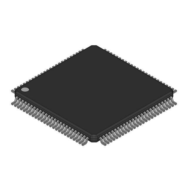
100-Pin TQFP
NC,DPb
DQb
DQb
VDDQ
VSSQ
DQb
DQb
DQb
DQb
VSSQ
VDDQ
DQb
DQb
VSS
NC
VDD
ZZ
DQa
DQa
VDDQ
VSSQ
DQa
DQa
DQa
DQa
VSSQ
VDDQ
DQa
DQa
NC,DPa
NC
NC
NC
VDDQ
VSSQ
NC
NC
DQb
DQb
VSSQ
VDDQ
DQb
DQb
NC
VDD
NC
VSS
DQb
DQb
VDDQ
VSSQ
DQb
DQb
DPb
NC
VSSQ
VDDQ
NC
NC
NC
1
2
3
4
5
6
7
8
9
10
11
12
13
14
15
16
17
18
19
20
21
22
23
24
25
26
27
28
29
30
CY7C1383B
(1 Mb x 18)
80
79
78
77
76
75
74
73
72
71
70
69
68
67
66
65
64
63
62
61
60
59
58
57
56
55
54
53
52
51
31
32
33
34
35
36
37
38
39
40
41
42
43
44
45
46
47
48
49
50
CY7C1381B
(512K X 36)
80
79
78
77
76
75
74
73
72
71
70
69
68
67
66
65
64
63
62
61
60
59
58
57
56
55
54
53
52
51
MODE
A
A
A
A
A1
A0
DNU
DNU
VSS
VDD
A
A
A
A
A
A
A
A
A
31
32
33
34
35
36
37
38
39
40
41
42
43
44
45
46
47
48
49
50
1
2
3
4
5
6
7
8
9
10
11
12
13
14
15
16
17
18
19
20
21
22
23
24
25
26
27
28
29
30
MODE
A
A
A
A
A1
A0
DNU
DNU
VSS
VDD
A
A
A
A
A
A
A
A
A
NC,DPc
DQc
DQc
VDDQ
VSSQ
DQc
DQc
DQc
DQc
VSSQ
VDDQ
DQc
DQc
NC
VDD
NC
VSS
DQd
DQd
VDDQ
VSSQ
DQd
DQd
DQd
DQd
VSSQ
VDDQ
DQd
DQd
NC,DPd
3
A
NC
NC
VDDQ
VSSQ
NC
DPa
DQa
DQa
VSSQ
VDDQ
DQa
DQa
VSS
NC
VDD
ZZ
DQa
DQa
VDDQ
VSSQ
DQa
DQa
NC
NC
VSSQ
VDDQ
NC
NC
NC
�CY7C1381B
CY7C1383B
PRELIMINARY
Pin Configurations (continued)
119-Ball BGA
CY7C1381B (512K x 36)
1
2
A
VDDQ
A
3
A
4
ADSP
5
A
6
A
7
VDDQ
B
NC
A
A
ADSC
A
A
NC
C
NC
A
A
VDD
A
A
NC
D
DQc
DQPc
VSS
NC
VSS
DQPb
DQb
E
DQc
DQc
VSS
CE1
VSS
DQb
DQb
F
VDDQ
DQc
VSS
OE
VSS
DQb
VDDQ
G
H
J
DQc
DQc
VDDQ
DQc
DQc
VDD
BWc
VSS
NC
ADV
GW
VDD
BWb
VSS
NC
DQb
DQb
VDD
DQb
DQb
VDDQ
K
L
M
DQd
DQd
VDDQ
DQd
DQd
DQd
VSS
BWd
VSS
CLK
NC
BWE
VSS
BWa
VSS
DQa
DQa
DQa
DQa
DQa
VDDQ
N
DQd
DQd
VSS
A1
VSS
DQa
DQa
P
DQd
DQPd
VSS
A0
VSS
DQPa
DQa
R
NC
VDD
NC
A
NC
NC
A
NC
MODE
T
A
A
A
NC
ZZ
U
VDDQ
TMS
TDI
TCK
TDO
NC
VDDQ
CY7C1383B (1M x 18)
1
2
3
4
5
6
7
A
VDDQ
A
A
ADSP
A
A
VDDQ
B
NC
A
A
ADSC
A
A
NC
C
NC
A
A
VDD
A
A
NC
D
DQb
NC
VSS
NC
VSS
DQPa
NC
E
NC
DQb
VSS
CE1
VSS
NC
DQa
F
VDDQ
NC
VSS
OE
VSS
DQa
VDDQ
G
H
J
NC
DQb
VDDQ
DQb
NC
VDD
BWb
VSS
NC
ADV
GW
VDD
VSS
VSS
NC
NC
DQb
VDD
DQa
NC
VDDQ
K
L
NC
DQb
DQb
NC
VSS
VSS
CLK
NC
VSS
BWa
NC
DQa
DQa
NC
M
VDDQ
DQb
VSS
BWE
VSS
NC
VDDQ
N
DQb
NC
VSS
A1
VSS
DQa
NC
P
NC
DQPb
VSS
A0
VSS
NC
DQa
R
NC
A
MODE
VDD
NC
A
NC
T
U
NC
VDDQ
A
TMS
A
TDI
NC
TCK
A
TDO
A
NC
ZZ
VDDQ
4
�CY7C1381B
CY7C1383B
PRELIMINARY
Pin Definitions
Name
I/O
Description
A0
A1
A
InputSynchronous
Address Inputs used to select one of the address locations. Sampled at the
rising edge of the CLK if ADSP or ADSC is active LOW, and CE1, CE2, and
CE3 are sampled active. A[1:0] feed the 2-bit counter.
BWa
BWb
BWc
BWd
InputSynchronous
Byte Write Select Inputs, active LOW. Qualified with BWE to conduct byte
writes to the SRAM. Sampled on the rising edge of CLK.
GW
InputSynchronous
Global Write Enable Input, active LOW. When asserted LOW on the rising
edge of CLK, a global write is conducted (ALL bytes are written, regardless of
the values on BWa,b,c,d and BWE).
BWE
InputSynchronous
Byte Write Enable Input, active LOW. Sampled on the rising edge of CLK. This
signal must be asserted LOW to conduct a byte write.
CLK
Input-Clock
Clock Input. Used to capture all synchronous inputs to the device. Also used
to increment the burst counter when ADV is asserted LOW, during a burst
operation.
CE1
InputSynchronous
Chip Enable 1 Input, active LOW. Sampled on the rising edge of CLK. Used
in conjunction with CE2 and CE3 to select/deselect the device. ADSP is ignored if CE1 is HIGH.
CE2
InputSynchronous
Chip Enable 2 Input, active HIGH. Sampled on the rising edge of CLK. Used
in conjunction with CE1 and CE3 to select/deselect the device.(TQFP Only)
CE3
InputSynchronous
Chip Enable 3 Input, active LOW. Sampled on the rising edge of CLK. Used
in conjunction with CE1 and CE2 to select/deselect the device. (TQFP Only)
OE
InputAsynchronous
Output Enable, asynchronous input, active LOW. Controls the direction of the
I/O pins. When LOW, the I/O pins behave as outputs. When deasserted HIGH,
I/O pins are three-stated, and act as input data pins. OE is masked during the
first clock of a read cycle when emerging from a deselected state.
ADV
InputSynchronous
Advance Input signal, sampled on the rising edge of CLK. When asserted, it
automatically increments the address in a burst cycle.
ADSP
InputSynchronous
Address Strobe from Processor, sampled on the rising edge of CLK. When
asserted LOW, A is captured in the address registers. A[1:0] are also loaded
into the burst counter. When ADSP and ADSC are both asserted, only ADSP
is recognized. ASDP is ignored when CE1 is deasserted HIGH.
ADSC
InputSynchronous
Address Strobe from Controller, sampled on the rising edge of CLK. When
asserted LOW, A[x:0] is captured in the address registers. A[1:0] are also loaded
into the burst counter. When ADSP and ADSC are both asserted, only ADSP
is recognized.
MODE
InputStatic
Selects burst order. When tied to GND selects linear burst sequence. When
tied to VDDQ or left floating selects interleaved burst sequence. This is a strap
pin and should remain static during device operation.
ZZ
InputAsynchronous
ZZ “sleep” Input. This active HIGH input places the device in a non-time critical
“sleep” condition with data integrity preserved.
DQa, DQPa
DQb, DQPb
DQc, DQPc
DQd, DQPd
I/OSynchronous
Bidirectional Data I/O lines. As inputs, they feed into an on-chip data register
that is triggered by the rising edge of CLK. As outputs, they deliver the data
contained in the memory location specified by A during the previous clock rise
of the read cycle. The direction of the pins is controlled by OE. When OE is
asserted LOW, the pins behave as outputs. When HIGH, DQa–DQd and DQPa–DQPd are placed in a three-state condition.
TDO
JTAG serial
output
Synchronous
Serial data-out to the JTAG circuit. Delivers data on the negative edge of TCK
(BGA Only).
5
�CY7C1381B
CY7C1383B
PRELIMINARY
Pin Definitions
Name
I/O
Description
TDI
JTAG serial
input
Synchronous
Serial data-In to the JTAG circuit. Sampled on the rising edge of TCK (BGA
Only).
TMS
Test Mode Select
Synchronous
This pin controls the Test Access Port state machine. Sampled on the rising
edge of TCK (BGA Only).
TCK
JTAG serial
clock
Serial clock to the JTAG circuit (BGA Only).
VDD
Power Supply
VSS
Ground
Ground for the core of the device. Should be connected to ground of the system.
VDDQ
I/O Power
Supply
Power supply for the I/O circuitry. Should be connected to a 2.5V power supply.
VSSQ
I/O Ground
Ground for the I/O circuitry. Should be connected to ground of the system.
NC
-
Power supply inputs to the core of the device. Should be connected to 2.5V
power supply.
No Connects.
6
�CY7C1381B
CY7C1383B
PRELIMINARY
will remain unaltered. All I/Os are three-stated during a byte
write because the CY7C1381B/CY7C1383B is a common I/O
device, the Output Enable (OE) must be deasserted HIGH before presenting data to the DQx inputs. Doing so will
three-state the output drivers. As a safety precaution, DQx are
automatically three-stated whenever a write cycle is detected,
regardless of the state of OE.
Functional Description
Single Read Accesses
This access is initiated when the following conditions are satisfied at clock rise: (1) ADSP or ADSC is asserted LOW, (2)
chip enable (CE1, CE2, CE3 on TQFP, CE1 on BGA) asserted
active, and (3) the write signals (GW, BWE) are all deasserted
HIGH. ADSP is ignored if CE1 is HIGH. The address presented
to the address inputs is stored into the address advancement
logic and the Address Register while being presented to the
memory core. If the OE input is asserted LOW, the requested
data will be available at the data outputs a maximum to tCDV
after clock rise. ADSP is ignored if CE1 is HIGH.
Burst Sequences
The CY7C1381B/CY7C1383B provides a two-bit wraparound
counter, fed by A[1:0], that implements either an interleaved or
linear burst sequence. to support processors that follow a linear burst sequence. The burst sequence is user selectable
through the MODE input.
Asserting ADV LOW at clock rise will automatically increment
the burst counter to the next address in the burst sequence.
Both read and write burst operations are supported.
Single Write Accesses Initiated by ADSP
This access is initiated when both of the following conditions
are satisfied at clock rise: (1) ADSP is asserted LOW, and (2)
Chip Enable asserted active. The address presented is loaded
into the address register and the address advancement logic
while being delivered to the RAM core. The write signals (GW,
BWE, and BWx) and ADV inputs are ignored during this first
clock cycle. If the write inputs are asserted active (see Write
Cycle Descriptions table for appropriate states that indicate a
write) on the next clock rise, the appropriate data will be
latched
and
written
into
the
device.
The
CY7C1381B/CY7C1383B provides byte write capability that is
described in the Write Cycle Description table. Asserting the
Byte Write Enable input (BWE) with the selected Byte Write
(BWa,b,c,d for CY7C1381B and BWa,b for CY7C1383B) input
will selectively write to only the desired bytes. Bytes not selected during a byte write operation will remain unaltered. All I/Os
are three-stated during a byte write.
Interleaved Burst Sequence
First
Address
Second
Address
Third
Address
Fourth
Address
A[1:0]
A[1:0]
A[1:0]
A[1:0]
00
01
10
11
01
00
11
10
10
11
00
01
11
10
01
00
Linear Burst Sequence
First
Address
Because the CY7C1381B/CY7C1383B is a common I/O device, the Output Enable (OE) must be deasserted HIGH before
presenting data to the DQx inputs. Doing so will three-state the
output drivers. As a safety precaution, DQx are automatically
three-stated whenever a write cycle is detected, regardless of
the state of OE.
Single Write Accesses Initiated by ADSC
ADSC write accesses are initiated when the following conditions are satisfied: (1) ADSC is asserted LOW, (2) ADSP is
deasserted HIGH, (3) Chip Enable (CE1, CE2, CE3 on TQFP,
CE1 on BGA) asserted active, and (4) the appropriate combination of the write inputs (GW, BWE, and BWx) are asserted
active to conduct a write to the desired byte(s). ADSC is ignored if ADSP is active LOW.
Second
Address
Third
Address
Fourth
Address
A[1:0]
A[1:0]
A[1:0]
A[1:0]
00
01
10
11
01
10
11
00
10
11
00
01
11
00
01
10
Sleep Mode
The ZZ input pin is an asynchronous input. Asserting ZZ HIGH
places the SRAM in a power conservation “sleep” mode. Two
clock cycles are required to enter into or exit from this “sleep”
mode. While in this mode, data integrity is guaranteed. Accesses pending when entering the “sleep” mode are not considered valid nor is the completion of the operation guaranteed. The device must be deselected prior to entering the
“sleep” mode. Chip Enable (CE1, CE2, CE3, on TQFP, CE1 on
BGA), ADSP and ADSC must remain inactive for the duration
of tZZREC after the ZZ input returns LOW. Leaving ZZ unconnected defaults the device into an active state.
The address presented to A[17:0] is loaded into the address
register and the address advancement logic while being delivered to the RAM core. The ADV input is ignored during this
cycle. If a global write is conducted, the data presented to the
DQx is written into the corresponding address location in the
RAM core. If a byte write is conducted, only the selected bytes
are written. Bytes not selected during a byte write operation
7
�CY7C1381B
CY7C1383B
PRELIMINARY
ZZ Mode Electrical Characteristics
Parameter
ICCZZ
tZZS
tZZREC
Description
Test Conditions
Snooze mode
standby current
Min.
Max.
Unit
ZZ > VDD − 0.2V
15
mA
Device operation to
ZZ
ZZ > VDD − 0.2V
2tCYC
ns
ZZ recovery time
ZZ < 0.2V
2tCYC
ns
Cycle Descriptions[1, 2, 3]
Next Cycle
Add. Used
ZZ
CE3
CE2
CE1
ADSP
ADSC
ADV
OE
DQ
Write
Unselected
None
L
X
X
1
X
0
X
X
Hi-Z
X
Unselected
None
L
1
X
0
0
X
X
X
Hi-Z
X
Unselected
None
L
X
0
0
0
X
X
X
Hi-Z
X
Unselected
None
L
1
X
0
1
0
X
X
Hi-Z
X
Unselected
None
L
X
0
0
1
0
X
X
Hi-Z
X
Begin Read
External
L
0
1
0
0
X
X
X
Hi-Z
X
Begin Read
External
L
0
1
0
1
0
X
X
Hi-Z
Read
Continue Read
Next
L
X
X
X
1
1
0
1
Hi-Z
Read
Continue Read
Next
L
X
X
X
1
1
0
0
DQ
Read
Continue Read
Next
L
X
X
1
X
1
0
1
Hi-Z
Read
Continue Read
Next
L
X
X
1
X
1
0
0
DQ
Read
Suspend Read
Current
L
X
X
X
1
1
1
1
Hi-Z
Read
Suspend Read
Current
L
X
X
X
1
1
1
0
DQ
Read
Suspend Read
Current
L
X
X
1
X
1
1
1
Hi-Z
Read
Suspend Read
Current
L
X
X
1
X
1
1
0
DQ
Read
Begin Write
Current
L
X
X
X
1
1
1
X
Hi-Z
Write
Begin Write
Current
L
X
X
1
X
1
1
X
Hi-Z
Write
Begin Write
External
L
0
1
0
1
0
X
X
Hi-Z
Write
Continue Write
Next
L
X
X
X
1
1
0
X
Hi-Z
Write
Continue Write
Next
L
X
X
1
X
1
0
X
Hi-Z
Write
Suspend Write
Current
L
X
X
X
1
1
1
X
Hi-Z
Write
Suspend Write
Current
L
X
X
1
X
1
1
X
Hi-Z
Write
ZZ “sleep”
None
H
X
X
X
X
X
X
X
Hi-Z
X
Note:
1. X =”Don't Care”, 1 = HIGH, 0 = LOW.
2. The SRAM always initiates a read cycle when ADSP asserted, regardless of the state of GW, BWE, or BWx. Writes may occur only on subsequent clocks
after the ADSP or with the assertion of ADSC. As a result, OE must be driven HIGH prior to the start of the write cycle to allow the outputs to three-state. OE
is a “Don't Care” for the remainder of the write cycle.
3. OE is asynchronous and is not sampled with the clock rise. It is masked internally during write cycles. During a read cycle DQ = High-Z when OE is inactive
or when the device is deselected, and DQ = data when OE is active.
8
�CY7C1381B
CY7C1383B
PRELIMINARY
Write Cycle Description[1, 2, 3]
Function (CY7C1381B)
GW
BWE
BWd
BWc
BWb
BWa
Read
1
1
X
X
X
X
Read
1
0
1
1
1
1
Write Byte 0 - DQa
1
0
1
1
1
0
Write Byte 1 - DQb
1
0
1
1
0
1
Write Bytes 1, 0
1
0
1
1
0
0
Write Byte 2 - DQc
1
0
1
0
1
1
Write Bytes 2, 0
1
0
1
0
1
0
Write Bytes 2, 1
1
0
1
0
0
1
Write Bytes 2, 1, 0
1
0
1
0
0
0
Write Byte 3 - DQd
1
0
0
1
1
1
Write Bytes 3, 0
1
0
0
1
1
0
Write Bytes 3, 1
1
0
0
1
0
1
Write Bytes 3, 1, 0
1
0
0
1
0
0
Write Bytes 3, 2
1
0
0
0
1
1
Write Bytes 3, 2, 0
1
0
0
0
1
0
Write Bytes 3, 2, 1
1
0
0
0
0
1
Write All Bytes
1
0
0
0
0
0
Write All Bytes
0
X
X
X
X
X
Function (CY7C1383B)
Read
GW
BWE
BWb
BWa
1
1
X
X
Read
1
0
1
1
Write Byte 0 - DQa and DPa
1
0
1
0
Write Byte 1 - DQb and DPb
1
0
0
1
Write All Bytes
1
0
0
0
Write All Bytes
0
X
X
X
9
�PRELIMINARY
IEEE 1149.1 Serial Boundary Scan (JTAG)
CY7C1381B
CY7C1383B
ry. Only one register can be selected at a time through the
instruction registers. Data is serially loaded into the TDI pin on
the rising edge of TCK. Data is output on the TDO pin on the
falling edge of TCK.
The CY7C1381B/CY7C1383B incorporates a serial boundary
scan Test Access Port (TAP) in the FBGA package only. The
TQFP package does not offer this functionality. This port operates in accordance with IEEE Standard 1149.1-1900, but does
not have the set of functions required for full 1149.1 compliance. These functions from the IEEE specification are excluded because their inclusion places an added delay in the critical
speed path of the SRAM. Note that the TAP controller functions in a manner that does not conflict with the operation of
other devices using 1149.1 fully compliant TAPs. The TAP operates using JEDEC standard 3.3V I/O logic levels.
Instruction Register
Three-bit instructions can be serially loaded into the instruction register. This register is loaded when it is placed between
the TDI and TDO pins as shown in the TAP Controller Block
Diagram. Upon power-up, the instruction register is loaded
with the IDCODE instruction. It is also loaded with the IDCODE
instruction if the controller is placed in a reset state as described in the previous section.
Disabling the JTAG Feature
When the TAP controller is in the CaptureIR state, the two least
significant bits are loaded with a binary "01" pattern to allow
for fault isolation of the board level serial test path.
It is possible to operate the SRAM without using the JTAG
feature. To disable the TAP controller, TCK must be tied LOW
(VSS) to prevent clocking of the device. TDI and TMS are internally pulled up and may be unconnected. They may alternately
be connected to VDD through a pull-up resistor. TDO should
be left unconnected. Upon power-up, the device will come up
in a reset state which will not interfere with the operation of the
device.
Bypass Register
To save time when serially shifting data through registers, it is
sometimes advantageous to skip certain states. The bypass
register is a single-bit register that can be placed between TDI
and TDO pins. This allows data to be shifted through the
SRAM with minimal delay. The bypass register is set LOW
(VSS) when the BYPASS instruction is executed.
Test Access Port (TAP) - Test Clock
The test clock is used only with the TAP controller. All inputs
are captured on the rising edge of TCK. All outputs are driven
from the falling edge of TCK.
Boundary Scan Register
The boundary scan register is connected to all the input and
output pins on the SRAM. Several no connect (NC) pins are
also included in the scan register to reserve pins for higher
density devices. The x36 configuration has a xx-bit-long register, and the x18 configuration has a yy-bit-long register.
Test Mode Select
The TMS input is used to give commands to the TAP controller
and is sampled on the rising edge of TCK. It is allowable to
leave this pin unconnected if the TAP is not used. The pin is
pulled up internally, resulting in a logic HIGH level.
The boundary scan register is loaded with the contents of the
RAM Input and Output ring when the TAP controller is in the
Capture-DR state and is then placed between the TDI and
TDO pins when the controller is moved to the Shift-DR state.
The EXTEST, SAMPLE/PRELOAD and SAMPLE Z instructions can be used to capture the contents of the Input and
Output ring.
Test Data-In (TDI)
The TDI pin is used to serially input information into the registers and can be connected to the input of any of the registers.
The register between TDI and TDO is chosen by the instruction that is loaded into the TAP instruction register. For information on loading the instruction register, see the TAP Controller State Diagram. TDI is internally pulled up and can be
unconnected if the TAP is unused in an application. TDI is connected to the Most Significant Bit (MSB) on any register.
The Boundary Scan Order tables show the order in which the
bits are connected. Each bit corresponds to one of the bumps
on the SRAM package. The MSB of the register is connected
to TDI, and the LSB is connected to TDO.
Identification (ID) Register
Test Data Out (TDO)
The TDO output pin is used to serially clock data-out from the
registers. The e output is active depending upon the current
state of the TAP state machine (see TAP Controller State
Diagram). The output changes on the falling edge of TCK.
TDO is connected to the Least Significant Bit (LSB) of any
register.
The ID register is loaded with a vendor-specific, 32-bit code
during the Capture-DR state when the IDCODE command is
loaded in the instruction register. The IDCODE is hardwired
into the SRAM and can be shifted out when the TAP controller
is in the Shift-DR state. The ID register has a vendor code and
other information described in the Identification Register Definitions table.
Performing a TAP Reset
TAP Instruction Set
A Reset is performed by forcing TMS HIGH (VDD) for five rising
edges of TCK. This RESET does not affect the operation of the
SRAM and may be performed while the SRAM is operating. At
power-up, the TAP is reset internally to ensure that TDO
comes up in a high-Z state.
Eight different instructions are possible with the three-bit instruction register. All combinations are listed in the Instruction
Code table. Three of these instructions are listed as RESERVED and should not be used. The other five instructions
are described in detail below.
TAP Registers
The TAP controller used in this SRAM is not fully compliant to
the 1149.1 convention because some of the mandatory 1149.1
instructions are not fully implemented. The TAP controller cannot be used to load address, data or control signals into the
Registers are connected between the TDI and TDO pins and
allow data to be scanned into and out of the SRAM test circuit-
10
�PRELIMINARY
SRAM and cannot preload the Input or Output buffers. The
SRAM does not implement the 1149.1 commands EXTEST or
INTEST or the PRELOAD portion of SAMPLE / PRELOAD;
rather it performs a capture of the Inputs and Output ring when
these instructions are executed.
CY7C1381B
CY7C1383B
When the SAMPLE / PRELOAD instructions loaded into the
instruction register and the TAP controller in the Capture-DR
state, a snapshot of data on the inputs and output pins is captured in the boundary scan register.
The user must be aware that the TAP controller clock can only
operate at a frequency up to 10 MHz, while the SRAM clock
operates more than an order of magnitude faster. Because
there is a large difference in the clock frequencies, it is possible
that during the Capture-DR state, an input or output will undergo a transition. The TAP may then try to capture a signal while
in transition (metastable state). This will not harm the device,
but there is no guarantee as to the value that will be captured.
Repeatable results may not be possible.
Instructions are loaded into the TAP controller during the
Shift-IR state when the instruction register is placed between
TDI and TDO. During this state, instructions are shifted
through the instruction register through the TDI and TDO pins.
To execute the instruction once it is shifted in, the TAP controller needs to be moved into the Update-IR state.
EXTEST
EXTEST is a mandatory 1149.1 instruction which is to be executed whenever the instruction register is loaded with all 0s.
EXTEST is not implemented in the TAP controller, and therefore this device is not compliant to the 1149.1 standard.
To guarantee that the boundary scan register will capture the
correct value of a signal, the SRAM signal must be stabilized
long enough to meet the TAP controller's capture set-up plus
hold times (TCS and TCH). The SRAM clock input might not
be captured correctly if there is no way in a design to stop (or
slow) the clock during a SAMPLE / PRELOAD instruction. If
this is an issue, it is still possible to capture all other signals
and simply ignore the value of the CK and CK captured in the
boundary scan register.
The TAP controller does recognize an all-0 instruction. When
an EXTEST instruction is loaded into the instruction register,
the SRAM responds as if a SAMPLE / PRELOAD instruction
has been loaded. There is one difference between the two
instructions. Unlike the SAMPLE / PRELOAD instruction, EXTEST places the SRAM outputs in a High-Z state.
Once the data is captured, it is possible to shift out the data by
putting the TAP into the Shift-DR state. This places the boundary scan register between the TDI and TDO pins.
IDCODE
The IDCODE instruction causes a vendor-specific, 32-bit code
to be loaded into the instruction register. It also places the
instruction register between the TDI and TDO pins and allows
the IDCODE to be shifted out of the device when the TAP controller enters the Shift-DR state. The IDCODE instruction is
loaded into the instruction register upon power-up or whenever
the TAP controller is given a test logic reset state.
Note that since the PRELOAD part of the command is not
implemented, putting the TAP into the Update to the
Update-DR state while performing a SAMPLE / PRELOAD instruction will have the same effect as the Pause-DR command.
Bypass
When the BYPASS instruction is loaded in the instruction register and the TAP is placed in a Shift-DR state, the bypass
register is placed between the TDI and TDO pins. The advantage of the BYPASS instruction is that it shortens the boundary
scan path when multiple devices are connected together on a
board.
SAMPLE Z
The SAMPLE Z instruction causes the boundary scan register
to be connected between the TDI and TDO pins when the TAP
controller is in a Shift-DR state. It also places all SRAM outputs
into a High-Z state.
Reserved
SAMPLE / PRELOAD
These instructions are not implemented but are reserved for
future use. Do not use these instructions.
SAMPLE / PRELOAD is a 1149.1 mandatory instruction. The
PRELOAD portion of this instruction is not implemented, so
the TAP controller is not fully 1149.1 compliant.
11
�CY7C1381B
CY7C1383B
PRELIMINARY
TAP Controller State Diagram
1
TEST-LOGIC
RESET
0
TEST-LOGIC/
IDLE
1
1
1
SELECT
DR-SCAN
SELECT
IR-SCAN
0
0
1
1
CAPTURE-DR
CAPTURE-DR
0
0
0
SHIFT-DR
0
SHIFT-IR
1
1
1
EXIT1-DR
1
EXIT1-IR
0
0
PAUSE-DR
0
0
PAUSE-IR
1
1
0
0
EXIT2-DR
EXIT2-IR
1
1
UPDATE-DR
1
0
Note: The 0/1 next to each state represents the value at TMS at the rising edge of TCK.
12
UPDATE-IR
1
0
�CY7C1381B
CY7C1383B
PRELIMINARY
TAP Controller Block Diagram
0
Bypass Register
Selection
Circuitry
2
TDI
1
0
1
0
1
0
Selection
Circuitry
TDO
Instruction Register
31 30
29
.
.
2
Identification Register
x
.
.
.
.
2
Boundary Scan Register
TCK
TAP Controller
TMS
TAP Electrical Characteristics Over the Operating Range[4, 5]
Parameter
Description
Test Conditions
Min.
Max.
Unit
VOH1
Output HIGH Voltage
IOH = –2.0 mA
1.7
V
VOH2
Output HIGH Voltage
IOH = –100 mA
2.1
V
VOL1
Output LOW Voltage
IOL = 2.0 mA
0.7
V
VOL2
Output LOW Voltage
IOL = 100 mA
0.2
V
VIH
Input HIGH Voltage
1.7
VDD+0.3
V
VIL
Input LOW Voltage
–0.3
0.7
V
IX
Input Load Current
–5
5
mA
4.
5.
GND < VI < VDDQ
All Voltage referenced to Ground.
Overshoot: VIH(AC)


 工商网监
湘ICP备2023018690号
工商网监
湘ICP备2023018690号
