CY7C1461SV33
36-Mbit (1M × 36) Flow-Through SRAM
with NoBL™ Architecture
36-Mbit (1M × 36) Flow-Through SRAM with NoBL™ Architecture
Features
Functional Description
■
No Bus Latency™ (NoBL™) architecture eliminates dead
cycles between write and read cycles
■
Supports up to 133-MHz bus operations with zero wait states
❐ Data is transferred on every clock
■
Pin-compatible and functionally equivalent to ZBT™ devices
■
Internally self timed output buffer control to eliminate the need
to use OE
■
Registered inputs for flow through operation
■
Byte Write capability
■
3.3 V/2.5 V I/O power supply
■
Fast clock-to-output times
❐ 6.5 ns (for 133-MHz device)
■
Clock Enable (CEN) pin to enable clock and suspend operation
■
Synchronous self timed writes
■
Asynchronous Output Enable
■
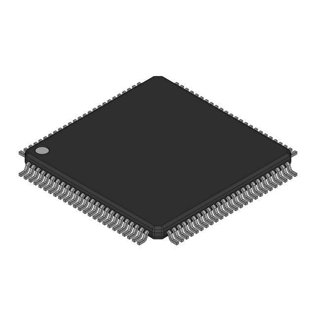
CY7C1461SV33 available in JEDEC-standard Pb-free 100-pin
TQFP package
■
Three chip enables for simple depth expansion
■
Automatic Power down feature available using ZZ mode or CE
deselect
■
Burst Capability – linear or interleaved burst order
■
Low standby power
The CY7C1461SV33 is a 3.3 V, 1M × 36 Synchronous Flow
-through Burst SRAM designed specifically to support unlimited
true back-to-back Read/Write operations without the insertion of
wait states. The CY7C1461SV33 is equipped with the advanced No
Bus Latency (NoBL) logic required to enable consecutive
Read/Write operations with data being transferred on every clock
cycle. This feature dramatically improves the throughput of data
through the SRAM, especially in systems that require frequent
Write-Read transitions.
All synchronous inputs pass through input registers controlled by
the rising edge of the clock. The clock input is qualified by the
Clock Enable (CEN) signal, which when deasserted suspends
operation and extends the previous clock cycle. Maximum
access delay from the clock rise is 6.5 ns (133-MHz device).
Write operations are controlled by the two or four Byte Write
Select (BWX) and a Write Enable (WE) input. All writes are
conducted with on-chip synchronous self timed write circuitry.
Three synchronous Chip Enables (CE1, CE2, CE3) and an
asynchronous Output Enable (OE) provide for easy bank
selection and output tri-state control. To avoid bus contention,
the output drivers are synchronously tri-stated during the data
portion of a write sequence.
Selection Guide
Description
133 MHz
Unit
Maximum Access Time
6.5
ns
Maximum Operating Current
310
mA
Maximum CMOS Standby Current
120
mA
Cypress Semiconductor Corporation
Document Number: 001-43801 Rev. *G
•
198 Champion Court
•
San Jose, CA 95134-1709
•
408-943-2600
Revised March 18, 2016
�CY7C1461SV33
Logic Block Diagram – CY7C1461SV33
ADDRESS
REGISTER
A0, A1, A
A1
D1
A0
D0
MODE
CLK
CEN
C
CE
ADV/LD
C
BURST
LOGIC
Q1 A1'
A0'
Q0
WRITE ADDRESS
REGISTER
ADV/LD
BW A
WRITE REGISTRY
AND DATA COHERENCY
CONTROL LOGIC
BW B
BW C
WRITE
DRIVERS
MEMORY
ARRAY
S
E
N
S
E
A
M
P
S
BW D
WE
OE
CE1
CE2
CE3
ZZ
INPUT
REGISTER
D
A
T
A
S
T
E
E
R
I
N
G
O
U
T
P
U
T
B
U
F
F
E
R
S
DQs
DQP A
DQP B
DQP C
DQP D
E
E
READ LOGIC
SLEEP
CONTROL
Document Number: 001-43801 Rev. *G
Page 2 of 21
�CY7C1461SV33
Contents
Pin Configurations ........................................................... 4
Pin Definitions .................................................................. 5
Functional Overview ........................................................ 6
Single Read Accesses ................................................ 6
Burst Read Accesses .................................................. 6
Single Write Accesses ................................................. 6
Burst Write Accesses .................................................. 7
Sleep Mode ................................................................. 7
Interleaved Burst Address Table ................................. 7
Linear Burst Address Table ......................................... 7
ZZ Mode Electrical Characteristics .............................. 7
Truth Table ........................................................................ 8
Truth Table for Read/Write .............................................. 9
Maximum Ratings ........................................................... 10
Neutron Soft Error Immunity ......................................... 10
Operating Range ............................................................. 10
Electrical Characteristics ............................................... 10
Capacitance .................................................................... 11
Document Number: 001-43801 Rev. *G
Thermal Resistance ........................................................ 11
AC Test Loads and Waveforms ..................................... 11
Switching Characteristics .............................................. 12
Switching Waveforms .................................................... 13
Ordering Information ...................................................... 16
Ordering Code Definitions ......................................... 16
Package Diagrams .......................................................... 17
Acronyms ........................................................................ 18
Document Conventions ................................................. 18
Units of Measure ....................................................... 18
Document History Page ................................................. 19
Sales, Solutions, and Legal Information ...................... 21
Worldwide Sales and Design Support ....................... 21
Products .................................................................... 21
PSoC® Solutions ...................................................... 21
Cypress Developer Community ................................. 21
Technical Support ..................................................... 21
Page 3 of 21
�CY7C1461SV33
Pin Configurations
A
40
41
42
43
44
45
46
47
48
49
50
NC/72M
A
A
A
A
A
A
A
A
37
A0
VSS
36
A1
VDD
35
A
39
34
A
NC/144M
33
A
38
32
NC/288M
31
Document Number: 001-43801 Rev. *G
81
A
82
A
83
A
84
ADV/LD
VSS
90
85
VDD
91
OE
CE3
92
86
BWA
93
CEN
BWB
94
WE
BWC
95
88
BWD
96
CLK
CE2
97
89
CE1
A
98
87
80
79
78
77
76
75
74
73
72
71
70
69
68
67
66
65
64
63
62
61
60
59
58
57
56
55
54
53
52
51
CY7C1461SV33
A
BYTE D
1
2
3
4
5
6
7
8
9
10
11
12
13
14
15
16
17
18
19
20
21
22
23
24
25
26
27
28
29
30
MODE
BYTE C
DQPC
DQC
DQC
VDDQ
VSS
DQC
DQC
DQC
DQC
VSS
VDDQ
DQC
DQC
NC
VDD
NC
VSS
DQD
DQD
VDDQ
VSS
DQD
DQD
DQD
DQD
VSS
VDDQ
DQD
DQD
DQPD
99
100
A
Figure 1. 100-pin TQFP (14 × 20 × 1.4 mm) pinout
DQPB
DQB
DQB
VDDQ
VSS
DQB
DQB
DQB
DQB
VSS
VDDQ
DQB
DQB
VSS
NC
VDD
ZZ
DQA
DQA
VDDQ
VSS
DQA
DQA
DQA
DQA
VSS
VDDQ
DQA
DQA
DQPA
BYTE B
BYTE A
Page 4 of 21
�CY7C1461SV33
Pin Definitions
Name
A0, A1, A
I/O
Description
InputAddress Inputs Used to Select one of the Address Locations. Sampled at the rising edge of the
Synchronous CLK. A[1:0] are fed to the two-bit burst counter.
InputByte Write Inputs, Active LOW. Qualified with WE to conduct writes to the SRAM. Sampled on the
BWA, BWB,
BWC, BWD Synchronous rising edge of CLK.
WE
InputWrite Enable Input, Active LOW. Sampled on the rising edge of CLK if CEN is active LOW. This signal
Synchronous must be asserted LOW to initiate a write sequence.
ADV/LD
InputAdvance/Load Input. Used to advance the on-chip address counter or load a new address. When HIGH
Synchronous (and CEN is asserted LOW) the internal burst counter is advanced. When LOW, a new address can be
loaded into the device for an access. After being deselected, ADV/LD must be driven LOW to load a
new address.
CLK
InputClock
Clock Input. Used to capture all synchronous inputs to the device. CLK is qualified with CEN. CLK is
only recognized if CEN is active LOW.
CE1
InputChip Enable 1 Input, Active LOW. Sampled on the rising edge of CLK. Used in conjunction with CE2
Synchronous and CE3 to select/deselect the device.
CE2
InputChip Enable 2 Input, Active HIGH. Sampled on the rising edge of CLK. Used in conjunction with CE1
Synchronous and CE3 to select/deselect the device.
CE3
InputChip Enable 3 Input, Active LOW. Sampled on the rising edge of CLK. Used in conjunction with CE1
Synchronous and CE2 to select/deselect the device.
OE
Output Enable, Asynchronous Input, Active LOW. Combined with the synchronous logic block inside
InputAsynchronou the device to control the direction of the I/O pins. When LOW, the I/O pins are allowed to behave as
outputs. When deasserted HIGH, I/O pins are tri-stated, and act as input data pins. OE is masked during
s
the data portion of a write sequence, during the first clock when emerging from a deselected state, when
the device is deselected.
CEN
InputClock Enable Input, Active LOW. When asserted LOW the Clock signal is recognized by the SRAM.
Synchronous When deasserted HIGH the Clock signal is masked. Since deasserting CEN does not deselect the
device, use CEN to extend the previous cycle when required.
ZZ
ZZ “Sleep” Input. This active HIGH input places the device in a non-time critical “sleep” condition with
InputAsynchronou data integrity preserved. During normal operation, this pin must be LOW or left floating. ZZ pin has an
internal pull down.
s
DQs
I/OBidirectional Data I/O Lines. As inputs, they feed into an on-chip data register that is triggered by the
Synchronous rising edge of CLK. As outputs, they deliver the data contained in the memory location specified by the
addresses presented during the previous clock rise of the read cycle. The direction of the pins is
controlled by OE. When OE is asserted LOW, the pins behave as outputs. When HIGH, DQs and
DQP[A:D] are placed in a tri-state condition.The outputs are automatically tri-stated during the data portion
of a write sequence, during the first clock when emerging from a deselected state, and when the device
is deselected, regardless of the state of OE.
DQPX
I/OBidirectional Data Parity I/O Lines. Functionally, these signals are identical to DQs. During write
Synchronous sequences, DQPX is controlled by BWX correspondingly.
MODE
VDD
VDDQ
Input Strap
Pin
Mode Input. Selects the Burst Order of the Device.
When tied to Gnd selects linear burst sequence. When tied to VDD or left floating selects interleaved
burst sequence.
Power Supply Power Supply Inputs to the Core of the Device.
I/O Power
Supply
Power Supply for the I/O Circuitry.
VSS
Ground
Ground for the Device.
NC
N/A
No Connects. Not internally connected to the die.
NC/72M
N/A
Not Connected to the Die. Can be tied to any voltage level.
Document Number: 001-43801 Rev. *G
Page 5 of 21
�CY7C1461SV33
Pin Definitions (continued)
Name
I/O
Description
NC/144M
N/A
Not Connected to the Die. Can be tied to any voltage level.
NC/288M
N/A
Not Connected to the Die. Can be tied to any voltage level.
NC/576M
N/A
Not Connected to the Die. Can be tied to any voltage level.
NC/1G
N/A
Not Connected to the Die. Can be tied to any voltage level.
Functional Overview
The CY7C1461SV33 is a synchronous flow through burst SRAM
designed specifically to eliminate wait states during Write-Read
transitions. All synchronous inputs pass through input registers
controlled by the rising edge of the clock. The clock signal is
qualified with the Clock Enable input signal (CEN). If CEN is
HIGH, the clock signal is not recognized and all internal states
are maintained. All synchronous operations are qualified with
CEN. Maximum access delay from the clock rise (tCDV) is 6.5 ns
(133-MHz device).
Accesses can be initiated by asserting all three Chip Enables
(CE1, CE2, CE3) active at the rising edge of the clock. If Clock
Enable (CEN) is active LOW and ADV/LD is asserted LOW, the
address presented to the device is latched. The access can
either be a read or write operation, depending on the status of
the Write Enable (WE). BWX can be used to conduct byte write
operations.
Write operations are qualified by the Write Enable (WE). All
writes are simplified with on-chip synchronous self timed write
circuitry.
Three synchronous Chip Enables (CE1, CE2, CE3) and an
asynchronous Output Enable (OE) simplify depth expansion. All
operations (Reads, Writes, and Deselects) are pipelined.
ADV/LD must be driven LOW after the device has been
deselected to load a new address for the next operation.
Single Read Accesses
A read access is initiated when these conditions are satisfied at
clock rise:
■
CEN is asserted LOW
■
CE1, CE2, and CE3 are ALL asserted active
■
The Write Enable input signal WE is deasserted HIGH
■
ADV/LD is asserted LOW.
The address presented to the address inputs is latched into the
Address Register and presented to the memory array and control
logic. The control logic determines that a read access is in
progress and allows the requested data to propagate to the
output buffers. The data is available within 6.5 ns (133-MHz
device) provided OE is active LOW. After the first clock of the
read access, the output buffers are controlled by OE and the
internal control logic. OE must be driven LOW in order for the
device to drive out the requested data. On the subsequent clock,
another operation (Read/Write/Deselect) can be initiated. When
the SRAM is deselected at clock rise by one of the chip enable
signals, its output is tri-stated immediately.
Document Number: 001-43801 Rev. *G
Burst Read Accesses
The CY7C1461SV33 has an on-chip burst counter that allows
the user the ability to supply a single address and conduct up to
four Reads without reasserting the address inputs. ADV/LD must
be driven LOW to load a new address into the SRAM, as
described in the Single Read Accesses section. The sequence
of the burst counter is determined by the MODE input signal. A
LOW input on MODE selects a linear burst mode, a HIGH selects
an interleaved burst sequence. Both burst counters use A0 and
A1 in the burst sequence, and wraps around when incremented
sufficiently. A HIGH input on ADV/LD increments the internal
burst counter regardless of the state of chip enable inputs or WE.
WE is latched at the beginning of a burst cycle. Therefore, the
type of access (Read or Write) is maintained throughout the burst
sequence.
Single Write Accesses
Write access are initiated when the following conditions are
satisfied at clock rise: (1) CEN is asserted LOW, (2) CE1, CE2,
and CE3 are ALL asserted active, and (3) the write signal WE is
asserted LOW. The address presented to the address bus is
loaded into the Address Register. The write signals are latched
into the Control Logic block. The data lines are automatically
tri-stated regardless of the state of the OE input signal. This
allows the external logic to present the data on DQs and DQPX.
On the next clock rise the data presented to DQs and DQPX (or
a subset for byte write operations, see truth table for details)
inputs is latched into the device and the write is complete.
Additional accesses (Read/Write/Deselect) can be initiated on
this cycle.
The data written during the Write operation is controlled by BWX
signals. The CY7C1461SV33 provides byte write capability that is
described in the truth table. Asserting the Write Enable input
(WE) with the selected Byte Write Select input selectively writes
to only the desired bytes. Bytes not selected during a byte write
operation remains unaltered. A synchronous self timed write
mechanism has been provided to simplify the write operations.
Byte write capability has been included to greatly simplify
Read/Modify/Write sequences, which can be reduced to simple
byte write operations.
Because the CY7C1461SV33 is a common I/O device, data must
not be driven into the device while the outputs are active. The
Output Enable (OE) can be deasserted HIGH before presenting
data to the DQs and DQPX inputs. Doing so tri-states the output
drivers. As a safety precaution, DQs and DQPX are automatically
tri-stated during the data portion of a write cycle, regardless of
the state of OE.
Page 6 of 21
�CY7C1461SV33
Burst Write Accesses
The CY7C1461SV33 has an on-chip burst counter that allows
the user the ability to supply a single address and conduct up to
four Write operations without reasserting the address inputs.
ADV/LD must be driven LOW to load the initial address, as
described in the section Single Write Accesses on page 6. When
ADV/LD is driven HIGH on the subsequent clock rise, the Chip
Enables (CE1, CE2, and CE3) and WE inputs are ignored and the
burst counter is incremented. The correct BWX inputs must be
driven in each cycle of the burst write, to write the correct bytes
of data.
Interleaved Burst Address Table
(MODE = Floating or VDD)
Sleep Mode
The ZZ input pin is an asynchronous input. Asserting ZZ places
the SRAM in a power conservation “sleep” mode. Two clock
cycles are required to enter into or exit from this “sleep” mode.
While in this mode, data integrity is guaranteed. Accesses
pending when entering the “sleep” mode are not considered valid
nor is the completion of the operation guaranteed. The device
must be deselected prior to entering the “sleep” mode. CE1, CE2,
and CE3, must remain inactive for the duration of tZZREC after the
ZZ input returns LOW.
First
Address
A1:A0
Second
Address
A1:A0
Third
Address
A1:A0
Fourth
Address
A1:A0
00
01
10
11
01
00
11
10
10
11
00
01
11
10
01
00
Fourth
Address
A1:A0
Linear Burst Address Table
(MODE = GND)
First
Address
A1:A0
Second
Address
A1:A0
Third
Address
A1:A0
00
01
10
11
01
10
11
00
10
11
00
01
11
00
01
10
ZZ Mode Electrical Characteristics
Parameter
Description
Test Conditions
Min
Max
Unit
IDDZZ
Sleep mode standby current
ZZ > VDD– 0.2 V
–
100
mA
tZZS
Device operation to ZZ
ZZ > VDD – 0.2 V
–
2tCYC
ns
tZZREC
ZZ recovery time
ZZ < 0.2 V
2tCYC
–
ns
tZZI
ZZ active to sleep current
This parameter is sampled
–
2tCYC
ns
tRZZI
ZZ Inactive to exit sleep current
This parameter is sampled
0
–
ns
Document Number: 001-43801 Rev. *G
Page 7 of 21
�CY7C1461SV33
Truth Table
The truth table for CY7C1461SV33 follows. [1, 2, 3, 4, 5, 6, 7]
Operation
Address Used CE1 CE2 CE3 ZZ ADV/LD WE BWX OE CEN
CLK
DQ
Deselect Cycle
None
H
X
X
L
L
X
X
X
L
L–>H
Tri-State
Deselect Cycle
None
X
X
H
L
L
X
X
X
L
L–>H
Tri-State
Deselect Cycle
None
X
L
X
L
L
X
X
X
L
L–>H
Tri-State
Continue Deselect Cycle
None
X
X
X
L
H
X
X
X
L
L–>H
Tri-State
Read Cycle (Begin Burst)
External
L
H
L
L
L
H
X
L
L
L–>H Data Out (Q)
Next
X
X
X
L
H
X
X
L
L
L–>H Data Out (Q)
External
L
H
L
L
L
H
X
H
L
L–>H
Tri-State
Next
X
X
X
L
H
X
X
H
L
L–>H
Tri-State
External
L
H
L
L
L
L
L
X
L
L–>H
Data In (D)
Write Cycle (Continue Burst)
Next
X
X
X
L
H
X
L
X
L
L–>H
Data In (D)
NOP/Write Abort (Begin Burst)
None
L
H
L
L
L
L
H
X
L
L–>H
Tri-State
Write Abort (Continue Burst)
Next
X
X
X
L
H
X
H
X
L
L–>H
Tri-State
Current
X
X
X
L
X
X
X
X
H
L–>H
–
None
X
X
X
H
X
X
X
X
X
X
Tri-State
Read Cycle (Continue Burst)
NOP/Dummy Read (Begin Burst)
Dummy Read (Continue Burst)
Write Cycle (Begin Burst)
Ignore Clock Edge (Stall)
Sleep Mode
Notes
1. X = “Don't Care.” H = Logic HIGH, L = Logic LOW. BWx = L signifies at least one Byte Write Select is active, BWx = Valid signifies that the desired byte write selects
are asserted, see truth table for details.
2. Write is defined by BWX, and WE. See truth table for Read/Write.
3. When a write cycle is detected, all IOs are tri-stated, even during byte writes.
4. The DQs and DQPX pins are controlled by the current cycle and the OE signal. OE is asynchronous and is not sampled with the clock.
5. CEN = H, inserts wait states.
6. Device powers up deselected and the IOs in a tri-state condition, regardless of OE.
7. OE is asynchronous and is not sampled with the clock rise. It is masked internally during write cycles. During a read cycle DQs and DQPX = Tri-state when OE is
inactive or when the device is deselected, and DQs and DQPX = data when OE is active.
Document Number: 001-43801 Rev. *G
Page 8 of 21
�CY7C1461SV33
Truth Table for Read/Write
The read/write truth table for CY7C1461SV33 follows.[8, 9]
Function (CY7C1461SV33)
WE
BWA
BWB
BWC
BWD
Read
H
X
X
X
X
Write No bytes written
L
H
H
H
H
Write Byte A – (DQA and DQPA)
L
L
H
H
H
Write Byte B – (DQB and DQPB)
L
H
L
H
H
Write Byte C – (DQC and DQPC)
L
H
H
L
H
Write Byte D – (DQD and DQPD)
L
H
H
H
L
Write All Bytes
L
L
L
L
L
Notes
8. X = “Don't Care.” H = Logic HIGH, L = Logic LOW. BWx = L signifies at least one Byte Write Select is active, BWx = Valid signifies that the desired byte write selects
are asserted, see truth table for details.
9. Table only lists a partial listing of the byte write combinations. Any Combination of BWX is valid Appropriate write is done based on which byte write is active
Document Number: 001-43801 Rev. *G
Page 9 of 21
�CY7C1461SV33
Maximum Ratings
Exceeding maximum ratings may impair the useful life of the
device. These user guidelines are not tested.
Storage Temperature ............................... –65 C to +150 C
Ambient Temperature with
Power Applied ......................................... –55C to +125 C
Supply Voltage on VDD Relative to GND .....–0.5 V to +4.6 V
Supply Voltage on VDDQ Relative to GND .... –0.5 V to +VDD
DC Voltage Applied to Outputs
in Tri-State ........................................–0.5 V to VDDQ + 0.5 V
Neutron Soft Error Immunity
Test
Conditions Typ
Parameter
Description
Max*
Unit
LSBU
Logical
Single-Bit
Upsets
25 °C
197
216
FIT/
Mb
LMBU
Logical
Multi-Bit
Upsets
25 °C
0
0.01
FIT/
Mb
SEL
Single Event
Latchup
85 °C
0
0.1
FIT/
Dev
Current into Outputs (LOW) ........................................ 20 mA
* No LMBU or SEL events occurred during testing; this column represents a
statistical 2, 95% confidence limit calculation. For more details refer to Application
Note AN54908 “Accelerated Neutron SER Testing and Calculation of Terrestrial
Failure Rates”.
Static Discharge Voltage
(MIL-STD-883, Method 3015) ................................. > 2001 V
Operating Range
DC Input Voltage ................................ –0.5 V to VDD + 0.5 V
Latch-up Current .................................................... > 200 mA
Range
Ambient
Temperature
Commercial
0 °C to +70 °C
VDD
VDDQ
3.3 V– 5% / 2.5 V – 5% to
VDD
+ 10%
Electrical Characteristics
Over the Operating Range
Parameter [10, 11]
Description
VDD
Power Supply Voltage
I/O Supply Voltage
VDDQ
VOH
VOL
VIH
VIL
IX
IOZ
IDD [12]
ISB1
Test Conditions
for 3.3 V I/O
for 2.5 V I/O
Output HIGH Voltage
for 3.3 V I/O, IOH = –4.0 mA
for 2.5 V I/O, IOH = –1.0 mA
Output LOW Voltage
for 3.3 V I/O, IOL = 8.0 mA
for 2.5 V I/O, IOL = 1.0 mA
Input HIGH Voltage[10]
for 3.3 V I/O
for 2.5 V I/O
Input LOW Voltage[10]
for 3.3 V I/O
for 2.5 V I/O
Input Leakage Current except ZZ GND VI VDDQ
and MODE
Input Current of MODE
Input = VSS
Input = VDD
Input Current of ZZ
Input = VSS
Input = VDD
Output Leakage Current
GND VI VDDQ, Output Disabled
VDD Operating Supply Current
VDD = Max., IOUT = 0 mA,
7.5 ns cycle,
f = fMAX = 1/tCYC
133 MHz
Automatic CE Power down
VDD = Max, Device Deselected, 7.5 ns cycle,
133 MHz
Current – TTL Inputs
VIN VIH or VIN VIL,
f = fMAX, inputs switching
Min
3.135
3.135
2.375
2.4
2.0
–
–
2.0
1.7
–0.3
–0.3
–5
Max
Unit
3.6
V
VDD
V
2.625
V
–
V
–
V
0.4
V
0.4
V
VDD + 0.3 V
V
VDD + 0.3 V
V
0.8
V
0.7
V
5
A
–30
–
–5
–
–5
–
–
5
–
30
5
310
A
A
A
A
A
mA
–
180
mA
Notes
10. Overshoot: VIH(AC) < VDD + 1.5 V (Pulse width less than tCYC/2), undershoot: VIL(AC) > –2 V (Pulse width less than tCYC/2).
11. TPower-up: Assumes a linear ramp from 0 V to VDD(min.) within 200 ms. During this time VIH < VDD and VDDQ < VDD.
12. The operation current is calculated with 50% read cycle and 50% write cycle.
Document Number: 001-43801 Rev. *G
Page 10 of 21
�CY7C1461SV33
Electrical Characteristics (continued)
Over the Operating Range
Parameter [10, 11]
Description
ISB2
Automatic CE Power down
Current – CMOS Inputs
ISB3
Automatic CE Power down
Current – CMOS Inputs
ISB4
Automatic CE Power down
Current – TTL Inputs
Test Conditions
VDD = Max, Device Deselected,
VIN 0.3 V or VIN > VDD – 0.3 V,
f = 0, inputs static
VDD = Max, Device Deselected,
VIN 0.3 V or VIN > VDDQ – 0.3 V,
f = fMAX, inputs switching
VDD = Max, Device Deselected,
VIN VDD – 0.3 V or VIN 0.3 V,
f = 0, inputs static
Min
Max
Unit
7.5 ns cycle,
133 MHz
–
120
mA
7.5 ns cycle,
133 MHz
–
180
mA
7.5 ns cycle,
133 MHz
–
135
mA
Capacitance
Parameter [13]
Description
100-pin TQFP Unit
Max
Test Conditions
TA = 25 C, f = 1 MHz,
VDD = 3.3 V, VDDQ = 2.5 V
CIN
Input capacitance
CCLK
Clock input capacitance
CIO
Input/Output capacitance
6.5
pF
3
pF
5.5
pF
Test Conditions
100-pin TQFP
Package
Unit
Test conditions follow standard test methods and
procedures for measuring thermal impedance, according
to EIA/JESD51.
25.21
°C/W
2.28
°C/W
Thermal Resistance
Parameter [13]
Description
JA
Thermal resistance
(junction to ambient)
JC
Thermal resistance
(junction to case)
AC Test Loads and Waveforms
Figure 2. AC Test Loads and Waveforms
3.3V I/O Test Load
3.3V
OUTPUT
R = 317
VT = 1.5V
(a)
5 pF
INCLUDING
JIG AND
SCOPE
2.5V I/O Test Load
2.5V
OUTPUT
GND
R = 351
VT = 1.25V
(a)
5 pF
INCLUDING
JIG AND
SCOPE
10%
90%
10%
90%
1ns
1ns
(b)
(c)
R = 1667
ALL INPUT PULSES
VDDQ
OUTPUT
RL = 50
Z0 = 50
ALL INPUT PULSES
VDDQ
OUTPUT
RL = 50
Z0 = 50
GND
R = 1538
(b)
10%
90%
10%
90%
1ns
1ns
(c)
Note
13. Tested initially and after any design or process change that may affect these parameters.
Document Number: 001-43801 Rev. *G
Page 11 of 21
�CY7C1461SV33
Switching Characteristics
Over the Operating Range
Parameter [14, 15]
Description
tPOWER[16]
133 MHz
Unit
Min
Max
1
–
ms
Clock
tCYC
Clock Cycle Time
7.5
–
ns
tCH
Clock HIGH
2.5
–
ns
tCL
Clock LOW
2.5
–
ns
Output Times
tCDV
Data Output Valid After CLK Rise
–
6.5
ns
tDOH
Data Output Hold After CLK Rise
2.5
–
ns
Z[17, 18, 19]
tCLZ
Clock to Low
2.5
–
ns
tCHZ
Clock to High Z[17, 18, 19]
–
3.8
ns
tOEV
OE LOW to Output Valid
–
3.0
ns
0
–
ns
–
3.0
ns
tOELZ
tOEHZ
OE LOW to Output Low
Z[17, 18, 19]
OE HIGH to Output High
Z[17, 18, 19]
Setup Times
tAS
Address Setup Before CLK Rise
1.5
–
ns
tALS
ADV/LD Setup Before CLK Rise
1.5
–
ns
tWES
WE, BWX Setup Before CLK Rise
1.5
–
ns
tCENS
CEN Setup Before CLK Rise
1.5
–
ns
tDS
Data Input Setup Before CLK Rise
1.5
–
ns
tCES
Chip Enable Setup Before CLK Rise
1.5
–
ns
tAH
Address Hold After CLK Rise
0.5
–
ns
tALH
ADV/LD Hold After CLK Rise
0.5
–
ns
tWEH
WE, BWX Hold After CLK Rise
0.5
–
ns
tCENH
CEN Hold After CLK Rise
0.5
–
ns
tDH
Data Input Hold After CLK Rise
0.5
–
ns
tCEH
Chip Enable Hold After CLK Rise
0.5
–
ns
Hold Times
Notes
14. Timing reference level is 1.5 V when VDDQ = 3.3 V and is 1.25 V when VDDQ = 2.5 V.
15. Test conditions shown in (a) of Figure 2 on page 11 unless otherwise noted.
16. This part has a voltage regulator internally; tPOWER is the time that the power is supplied above VDD(minimum) initially, before a read or write operation can be initiated.
17. tCHZ, tCLZ,tOELZ, and tOEHZ are specified with AC test conditions shown in part (b) of Figure 2 on page 11. Transition is measured ±200 mV from steady-state voltage.
18. At any voltage and temperature, tOEHZ is less than tOELZ and tCHZ is less than tCLZ to eliminate bus contention between SRAMs when sharing the same data bus.
These specifications do not imply a bus contention condition, but reflect parameters guaranteed over worst case user conditions. Device is designed to achieve High Z
prior to Low Z under the same system conditions.
19. This parameter is sampled and not 100% tested.
Document Number: 001-43801 Rev. *G
Page 12 of 21
�CY7C1461SV33
Switching Waveforms
Figure 3. Read/Write Waveforms [20, 21, 22]
1
2
3
t CYC
4
5
6
7
8
9
A5
A6
A7
10
CLK
t CENS
t CENH
t CES
t CEH
t CH
t CL
CEN
CE
ADV/LD
WE
BW X
A1
ADDRESS
t AS
A2
A4
A3
t CDV
t AH
t DOH
t CLZ
DQ
D(A1)
t DS
D(A2)
Q(A3)
D(A2+1)
t OEV
Q(A4+1)
Q(A4)
t OELZ
W RITE
D(A1)
W RITE
D(A2)
D(A5)
Q(A6)
D(A7)
W RITE
D(A7)
DESELECT
t OEHZ
t DH
OE
COM M AND
t CHZ
BURST
W RITE
D(A2+1)
READ
Q(A3)
READ
Q(A4)
DON’T CARE
BURST
READ
Q(A4+1)
t DOH
W RITE
D(A5)
READ
Q(A6)
UNDEFINED
Notes
20. For this waveform ZZ is tied LOW.
21. When CE is LOW, CE1 is LOW, CE2 is HIGH and CE3 is LOW. When CE is HIGH, CE1 is HIGH or CE2 is LOW or CE3 is HIGH.
22. Order of the Burst sequence is determined by the status of the MODE (0 = Linear, 1 = Interleaved). Burst operations are optional.
Document Number: 001-43801 Rev. *G
Page 13 of 21
�CY7C1461SV33
Switching Waveforms (continued)
Figure 4. NOP, STALL and DESELECT Cycles [23, 24, 25]
1
2
A1
A2
3
4
5
A3
A4
6
7
8
9
10
CLK
CEN
CE
ADV/LD
WE
BW [A:D]
ADDRESS
A5
t CHZ
D(A1)
DQ
Q(A2)
Q(A3)
D(A4)
Q(A5)
t DOH
COMMAND
WRITE
D(A1)
READ
Q(A2)
STALL
READ
Q(A3)
WRITE
D(A4)
DON’T CARE
STALL
NOP
READ
Q(A5)
DESELECT
CONTINUE
DESELECT
UNDEFINED
Notes
23. For this waveform ZZ is tied LOW.
24. When CE is LOW, CE1 is LOW, CE2 is HIGH and CE3 is LOW. When CE is HIGH, CE1 is HIGH or CE2 is LOW or CE3 is HIGH.
25. The IGNORE CLOCK EDGE or STALL cycle (Clock 3) illustrates CEN being used to create a pause. A write is not performed during this cycle.
Document Number: 001-43801 Rev. *G
Page 14 of 21
�CY7C1461SV33
Switching Waveforms (continued)
Figure 5. ZZ Mode Timing [26, 27]
CLK
t ZZ
ZZ
I
t ZZREC
t ZZI
SUPPLY
I DDZZ
t RZZI
ALL INPUTS
(except ZZ)
Outputs (Q)
DESELECT or READ Only
High-Z
DON’T CARE
Notes
26. Device must be deselected when entering ZZ mode. See truth table for all possible signal conditions to deselect the device.
27. DQs are in High Z when exiting ZZ sleep mode.
Document Number: 001-43801 Rev. *G
Page 15 of 21
�CY7C1461SV33
Ordering Information
Cypress offers other versions of this type of product in many different configurations and features. The following table contains only
the list of parts that are currently available. For a complete listing of all options, visit the Cypress website at www.cypress.com and
refer to the product summary page at http://www.cypress.com/products or contact your local sales representative.
Cypress maintains a worldwide network of offices, solution centers, manufacturer’s representatives and distributors. To find the office
closest to you, visit us at http://www.cypress.com/go/datasheet/offices.
Speed
(MHz)
133
Package
Diagram
Ordering Code
CY7C1461SV33-133AXC
Part and Package Type
51-85050 100-pin TQFP (14 × 20 × 1.4 mm) Pb-free
Operating
Range
Commercial
Ordering Code Definitions
CY 7
C 1461 S V33 - 133
A
X C
Temperature Range:
C = Commercial
Pb-free
Package Type:
AX = 100-pin TQFP
Frequency Range: 133 MHz
V33 = 3.3 V
Die Revision
Part Identifier: 1461 = FT, 1Mb × 36 (36 Mb)
Technology Code: C = CMOS
Marketing Code: 7 = SRAM
Company ID: CY = Cypress
Document Number: 001-43801 Rev. *G
Page 16 of 21
�CY7C1461SV33
Package Diagrams
Figure 6. 100-pin TQFP (14 × 20 × 1.4 mm) A100RA Package Outline, 51-85050
51-85050 *E
Document Number: 001-43801 Rev. *G
Page 17 of 21
�CY7C1461SV33
Acronyms
Acronym
Document Conventions
Description
Units of Measure
CMOS
Complementary Metal Oxide Semiconductor
I/O
Input/Output
°C
degree Celsius
LSB
Least Significant Bit
MHz
megahertz
MSB
Most Significant Bit
µA
microampere
OE
Output Enable
mA
milliampere
SRAM
Static Random Access Memory
mm
millimeter
TQFP
Thin Quad Flat Pack
ms
millisecond
TTL
Transistor-Transistor Logic
mV
millivolt
WE
Write Enable
ns
nanosecond
Document Number: 001-43801 Rev. *G
Symbol
Unit of Measure
ohm
%
percent
pF
picofarad
V
volt
W
watt
Page 18 of 21
�CY7C1461SV33
Document History Page
Document Title: CY7C1461SV33, 36-Mbit (1M × 36) Flow-Through SRAM with NoBL™ Architecture
Document Number: 001-43801
Rev.
ECN No.
Issue Date
Orig. of
Change
**
1897686
See ECN
VKN /
AESA
*A
2082846
See ECN
VKN
Changed status from Preliminary to Final.
*B
2899815
03/26/2010
NJY
Updated Ordering Information (Removed inactive parts) and updated the text
below the heading in Ordering Information table.
Added Neutron Soft Error Immunity.
Updated Package Diagrams.
*C
2905432
04/06/2010
VKN
Updated Ordering Information (Removed part number
CY7C1461SV33-133AXI).
*D
3205724
03/25/2011
NJY
Updated Ordering Information (Updated part numbers) and added Ordering
Code Definitions.
Updated Package Diagrams.
Added Acronyms and Units of Measure.
Updated to new template.
*E
3572553
04/04/2012
PRIT
Updated Features (Removed 165-ball FBGA package and 209-ball FBGA
package related information, removed JTAG related information).
Updated Functional Description (Removed CY7C1463SV33 and
CY7C1465SV33 related information, removed the Note “For best practices or
recommendations, please refer to the Cypress application note AN1064,
SRAM System Design Guidelines on www.cypress.com.” and its reference).
Updated Selection Guide (Removed 100 MHz frequency related information).
Removed Logic Block Diagram – CY7C1463SV33.
Removed Logic Block Diagram – CY7C1465SV33.
Updated Pin Configurations (Removed CY7C1463SV33 and CY7C1465SV33
related information, removed 165-ball FBGA package and 209-ball FBGA
package related information).
Updated Pin Definitions (Removed JTAG related information).
Updated Functional Overview (Removed CY7C1463SV33 and
CY7C1465SV33 related information).
Updated Truth Table (Removed CY7C1463SV33 and CY7C1465SV33 related
information).
Removed Truth Table for Read/Write (Corresponding to CY7C1463SV33 and
CY7C1465SV33).
Removed IEEE 1149.1 Serial Boundary Scan (JTAG).
Removed TAP Controller State Diagram.
Removed TAP Controller Block Diagram.
Removed TAP Timing.
Removed TAP AC Switching Characteristics.
Removed 3.3 V TAP AC Test Conditions.
Removed 3.3 V TAP AC Output Load Equivalent.
Removed 2.5 V TAP AC Test Conditions.
Removed 2.5 V TAP AC Output Load Equivalent.
Removed TAP DC Electrical Characteristics and Operating Conditions.
Removed Identification Register Definitions.
Removed Scan Register Sizes.
Removed Identification Codes.
Removed Boundary Scan Order.
Document Number: 001-43801 Rev. *G
Description of Change
New data sheet.
Page 19 of 21
�CY7C1461SV33
Document History Page (continued)
Document Title: CY7C1461SV33, 36-Mbit (1M × 36) Flow-Through SRAM with NoBL™ Architecture
Document Number: 001-43801
Rev.
ECN No.
Issue Date
Orig. of
Change
Description of Change
*E (cont.)
3572553
04/04/2012
PRIT
Updated Operating Range (Removed Industrial Temperature range).
Updated Electrical Characteristics (Removed 100 MHz frequency related
information).
Updated Capacitance (Removed 165-ball FBGA package and 209-ball FBGA
package related information).
Updated Thermal Resistance (Removed 165-ball FBGA package and 209-ball
FBGA package related information).
Updated Switching Characteristics (Removed 100 MHz frequency related
information).
Updated Package Diagrams (Removed 165-ball FBGA package and 209-ball
FBGA package related information).
Replaced all instances of IO with I/O across the document.
*F
3978170
04/22/2013
PRIT
No technical updates.
Completing Sunset Review.
*G
5181018
03/18/2016
PRIT
Updated Package Diagrams:
spec 51-85050 – Changed revision from *D to *E.
Updated to new template.
Completing Sunset Review.
Document Number: 001-43801 Rev. *G
Page 20 of 21
�CY7C1461SV33
Sales, Solutions, and Legal Information
Worldwide Sales and Design Support
Cypress maintains a worldwide network of offices, solution centers, manufacturer’s representatives, and distributors. To find the office
closest to you, visit us at Cypress Locations.
PSoC® Solutions
Products
ARM® Cortex® Microcontrollers
Automotive
cypress.com/arm
cypress.com/automotive
Clocks & Buffers
Interface
Lighting & Power Control
Memory
cypress.com/clocks
cypress.com/interface
cypress.com/powerpsoc
cypress.com/memory
PSoC
cypress.com/psoc
Touch Sensing
PSoC 1 | PSoC 3 | PSoC 4 | PSoC 5LP
Cypress Developer Community
Community | Forums | Blogs | Video | Training
Technical Support
cypress.com/support
cypress.com/touch
USB Controllers
Wireless/RF
cypress.com/psoc
cypress.com/usb
cypress.com/wireless
© Cypress Semiconductor Corporation 2008-2016. This document is the property of Cypress Semiconductor Corporation and its subsidiaries, including Spansion LLC ("Cypress"). This document,
including any software or firmware included or referenced in this document ("Software"), is owned by Cypress under the intellectual property laws and treaties of the United States and other countries
worldwide. Cypress reserves all rights under such laws and treaties and does not, except as specifically stated in this paragraph, grant any license under its patents, copyrights, trademarks, or other
intellectual property rights. If the Software is not accompanied by a license agreement and you do not otherwise have a written agreement with Cypress governing the use of the Software, then Cypress
hereby grants you under its copyright rights in the Software, a personal, non-exclusive, nontransferable license (without the right to sublicense) (a) for Software provided in source code form, to modify
and reproduce the Software solely for use with Cypress hardware products, only internally within your organization, and (b) to distribute the Software in binary code form externally to end users (either
directly or indirectly through resellers and distributors), solely for use on Cypress hardware product units. Cypress also grants you a personal, non-exclusive, nontransferable, license (without the right
to sublicense) under those claims of Cypress's patents that are infringed by the Software (as provided by Cypress, unmodified) to make, use, distribute, and import the Software solely to the minimum
extent that is necessary for you to exercise your rights under the copyright license granted in the previous sentence. Any other use, reproduction, modification, translation, or compilation of the Software
is prohibited.
CYPRESS MAKES NO WARRANTY OF ANY KIND, EXPRESS OR IMPLIED, WITH REGARD TO THIS DOCUMENT OR ANY SOFTWARE, INCLUDING, BUT NOT LIMITED TO, THE IMPLIED
WARRANTIES OF MERCHANTABILITY AND FITNESS FOR A PARTICULAR PURPOSE. Cypress reserves the right to make changes to this document without further notice. Cypress does not
assume any liability arising out of the application or use of any product or circuit described in this document. Any information provided in this document, including any sample design information or
programming code, is provided only for reference purposes. It is the responsibility of the user of this document to properly design, program, and test the functionality and safety of any application
made of this information and any resulting product. Cypress products are not designed, intended, or authorized for use as critical components in systems designed or intended for the operation of
weapons, weapons systems, nuclear installations, life-support devices or systems, other medical devices or systems (including resuscitation equipment and surgical implants), pollution control or
hazardous substances management, or other uses where the failure of the device or system could cause personal injury, death, or property damage ("Unintended Uses"). A critical component is any
component of a device or system whose failure to perform can be reasonably expected to cause the failure of the device or system, or to affect its safety or effectiveness. Cypress is not liable, in whole
or in part, and Company shall and hereby does release Cypress from any claim, damage, or other liability arising from or related to all Unintended Uses of Cypress products. Company shall indemnify
and hold Cypress harmless from and against all claims, costs, damages, and other liabilities, including claims for personal injury or death, arising from or related to any Unintended Uses of Cypress
products.
Cypress, the Cypress logo, Spansion, the Spansion logo, and combinations thereof, PSoC, CapSense, EZ-USB, F-RAM, and Traveo are trademarks or registered trademarks of Cypress in the United
States and other countries. For a more complete list of Cypress trademarks, visit cypress.com. Other names and brands may be claimed as property of their respective owners.
Document Number: 001-43801 Rev. *G
Revised March 18, 2016
NoBL and No Bus Latency are trademarks of Cypress Semiconductor Corporation. ZBT is a trademark of Integrated Device Technology, Inc.
Page 21 of 21
�