PRELIMINARY
CY7C1510V18 CY7C1525V18 CY7C1512V18 CY7C1514V18
72-Mbit QDR-II™ SRAM 2-Word Burst Architecture
Features
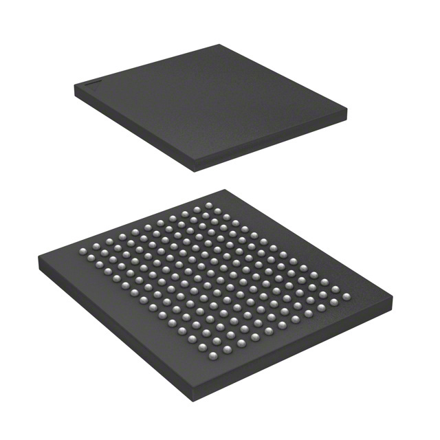
• Separate Independent Read and Write Data Ports — Supports concurrent transactions • 200-MHz clock for high bandwidth • 2-Word Burst on all accesses • Double Data Rate (DDR) interfaces on both Read and Write ports (data transferred at 400 MHz) @ 200 MHz • Two input clocks (K and K) for precise DDR timing — SRAM uses rising edges only • Two output clocks (C and C) accounts for clock skew and flight time mismatching • Echo clocks (CQ and CQ) simplify data capture in high speed systems • Single multiplexed address input bus latches address inputs for both Read and Write ports • Separate Port Selects for depth expansion • Synchronous internally self-timed writes • Available in x8, x9, x18, and x36 configurations • Full data coherency, providing most current data • Core VDD = 1.8V(±0.1V);I/O VDDQ = 1.4V to VDD • 15 × 17 × 1.4 mm 1.0-mm pitch FBGA package, 165-ball (11 × 15 matrix) • Variable drive HSTL output buffers • JTAG 1149.1 compatible test access port • Delay Lock Loop (DLL) for accurate data placement
Functional Description
The CY7C1510V18, CY7C1525V18, CY7C1512V18, and CY7C1514V18 are 1.8V Synchronous Pipelined SRAMs, equipped with QDR-II architecture. QDR-II architecture consists of two separate ports to access the memory array. The Read port has dedicated Data Outputs to support Read operations and the Write Port has dedicated Data Inputs to support Write operations. QDR-II architecture has separate data inputs and data outputs to completely eliminate the need to “turn-around” the data bus required with common I/O devices. Access to each port is accomplished through a common address bus. The Read address is latched on the rising edge of the K clock and the Write address is latched on the rising edge of the K clock. Accesses to the QDR-II Read and Write ports are completely independent of one another. In order to maximize data throughput, both Read and Write ports are equipped with Double Data Rate (DDR) interfaces. Each address location is associated with two 8-bit words (CY7C1510V18) or 9-bit words (CY7C1525V18) or 18-bit words (CY7C1512V18) or 36-bit words (CY7C1514V18) that burst sequentially into or out of the device. Since data can be transferred into and out of the device on every rising edge of both input clocks (K and K and C and C), memory bandwidth is maximized while simplifying system design by eliminating bus “turn-arounds.” Depth expansion is accomplished with Port Selects for each port. Port selects allow each port to operate independently. All synchronous inputs pass through input registers controlled by the K or K input clocks. All data outputs pass through output registers controlled by the C or C (or K or K in a single clock domain) input clocks. Writes are conducted with on-chip synchronous self-timed write circuitry.
Configurations
CY7C1510V18 – 8M x 8 CY7C1525V18 – 8M x 9 CY7C1512V18 – 4M x 18 CY7C1514V18 – 2M x 36
Cypress Semiconductor Corporation Document #: 38-05489 Rev. *A
•
3901 North First Street
•
San Jose, CA 95134
• 408-943-2600 Revised July 21, 2004
�PRELIMINARY
Logic Block Diagram (CY7C1510V18)
D[7:0] 8 Write Reg 4M x 8 Array
Write Add. Decode
CY7C1510V18 CY7C1525V18 CY7C1512V18 CY7C1514V18
22
Read Add. Decode
A(21:0)
Address Register
Write Reg 4M x 8 Array
Address Register
22
A(21:0)
K K
CLK Gen.
Control Logic
RPS C C
DOFF
Read Data Reg. 16 Control Logic 8 8 Reg. Reg. 8 Reg.
CQ CQ
VREF WPS NWS[1:0]
8 8 Q[7:0]
Logic Block Diagram (CY7C1525V18)
D[8:0] 9 Write Reg 4M x 9 Array
Write Add. Decode
22
Read Add. Decode
A(21:0)
Address Register
Write Reg 4M x 9 Array
Address Register
22
A(21:0)
K K
CLK Gen.
Control Logic
RPS C C
DOFF
Read Data Reg. 18 Control Logic 9 9 Reg. Reg. 9 Reg. 9
CQ CQ
VREF WPS BWS[0]
9Q [8:0]
Document #: 38-05489 Rev. *A
Page 2 of 24
�PRELIMINARY
Logic Block Diagram (CY7C1512V18)
D[17:0] 18 Write Reg 2M x 18 Array
Write Add. Decode
CY7C1510V18 CY7C1525V18 CY7C1512V18 CY7C1514V18
21
Read Add. Decode
A(20:0)
Address Register
Write Reg 2M x 18 Array
Address Register
21
A(20:0)
K K
CLK Gen.
Control Logic
RPS C C
DOFF
Read Data Reg. 36 Control Logic 18 18 Reg. Reg. 18 Reg.
CQ CQ
VREF WPS BWS[1:0]
18
18 Q[17:0]
Logic Block Diagram (CY7C1514V18)
D[35:0] 36 Write Reg 1M x 36 Array
Write Add. Decode
20
Read Add. Decode
A(19:0)
Address Register
Write Reg 1M x 36 Array
Address Register
20
A(19:0)
K K
CLK Gen.
Control Logic
RPS C C
DOFF
Read Data Reg. 72 Control Logic 36 36 Reg. Reg. 36 Reg.
CQ CQ
VREF WPS BWS[3:0]
36 36
Q[35:0]
Selection Guide
250 MHz Maximum Operating Frequency Maximum Operating Current 250 TBD 200 MHz 200 TBD 167 MHz 167 TBD Unit MHz mA
Shaded area contains advance information. Please contact your local Cypress Sales representative for availability of these parts.
Document #: 38-05489 Rev. *A
Page 3 of 24
�PRELIMINARY
Pin Configurations
CY7C1510V18 (8M × 8) – 15 × 17 FBGA
CY7C1510V18 CY7C1525V18 CY7C1512V18 CY7C1514V18
1 A B C D E F G H J K L M N P R
CQ NC NC NC NC NC NC DOFF NC NC NC NC NC NC TDO
2
A NC NC D4 NC NC D5 VREF NC NC Q6 NC D7 NC TCK
3
A NC NC NC Q4 NC Q5 VDDQ NC NC D6 NC NC Q7 A
4
WPS A VSS VSS VDDQ VDDQ VDDQ VDDQ VDDQ VDDQ VDDQ VSS VSS A A
5
NWS1 NC/288M A VSS VSS VDD VDD VDD VDD VDD VSS VSS A A A
6
K K A VSS VSS VSS VSS VSS VSS VSS VSS VSS A C C
7
NC/144M NWS0 A VSS VSS VDD VDD VDD VDD VDD VSS VSS A A A
8
RPS A VSS VSS VDDQ VDDQ VDDQ VDDQ VDDQ VDDQ VDDQ VSS VSS A A
9
A NC NC NC NC NC NC VDDQ NC NC NC NC NC NC A
10
A NC NC NC D2 NC NC VREF Q1 NC NC NC NC NC TMS
11
CQ Q3 D3 NC Q2 NC NC ZQ D1 NC Q0 D0 NC NC TDI
CY7C1525V18 (8M × 9)–11 × 15 Balls (15 × 17 FBGA)
1 A B C D E F G H J K L M N P R
CQ NC NC NC NC NC NC DOFF NC NC NC NC NC NC TDO
2
A NC NC D5 NC NC D6 VREF NC NC Q7 NC D8 NC TCK
3
A NC NC NC Q5 NC Q6 VDDQ NC NC D7 NC NC Q8 A
4
WPS A VSS VSS VDDQ VDDQ VDDQ VDDQ VDDQ VDDQ VDDQ VSS VSS A A
5
NC NC A VSS VSS VDD VDD VDD VDD VDD VSS VSS A A A
6
K K A VSS VSS VSS VSS VSS VSS VSS VSS VSS A C C
7
NC/144M BWS0 A VSS VSS VDD VDD VDD VDD VDD VSS VSS A A A
8
RPS A VSS VSS VDDQ VDDQ VDDQ VDDQ VDDQ VDDQ VDDQ VSS VSS A A
9
A NC NC NC NC NC NC VDDQ NC NC NC NC NC NC A
10
A NC NC NC D3 NC NC VREF Q2 NC NC NC NC D0 TMS
11
CQ Q4 D4 NC Q3 NC NC ZQ D2 NC Q1 D1 NC Q0 TDI
Document #: 38-05489 Rev. *A
Page 4 of 24
�PRELIMINARY
Pin Configurations (continued)
CY7C1512V18 (4M × 18) – 15 × 17 FBGA
CY7C1510V18 CY7C1525V18 CY7C1512V18 CY7C1514V18
1 A B C D E F G H J K L M N P R
CQ NC NC NC NC NC NC DOFF NC NC NC NC NC NC TDO
2
VSS/144M Q9 NC D11 NC Q12 D13 VREF NC NC Q15 NC D17 NC TCK
3
A D9 D10 Q10 Q11 D12 Q13 VDDQ D14 Q14 D15 D16 Q16 Q17 A
4
WPS A VSS VSS VDDQ VDDQ VDDQ VDDQ VDDQ VDDQ VDDQ VSS VSS A A
5
BWS1 NC A VSS VSS VDD VDD VDD VDD VDD VSS VSS A A A
6
K K A VSS VSS VSS VSS VSS VSS VSS VSS VSS A C C
7
NC/288M BWS0 A VSS VSS VDD VDD VDD VDD VDD VSS VSS A A A
8
RPS A VSS VSS VDDQ VDDQ VDDQ VDDQ VDDQ VDDQ VDDQ VSS VSS A A
9
A NC NC NC NC NC NC VDDQ NC NC NC NC NC NC A
10
A NC Q7 NC D6 NC NC VREF Q4 D3 NC Q1 NC D0 TMS
11
CQ Q8 D8 D7 Q6 Q5 D5 ZQ D4 Q3 Q2 D2 D1 Q0 TDI
CY7C1514V18 (2M × 36) – 15 × 17 FBGA
1 A B C D E F G H J K L M N P R
CQ Q27 D27 D28 Q29 Q30 D30 DOFF D31 Q32 Q33 D33 D34 Q35 TDO
2
Vss/288M Q18 Q28 D20 D29 Q21 D22 VREF Q31 D32 Q24 Q34 D26 D35 TCK
3
A D18 D19 Q19 Q20 D21 Q22 VDDQ D23 Q23 D24 D25 Q25 Q26 A
4
WPS A VSS VSS VDDQ VDDQ VDDQ VDDQ VDDQ VDDQ VDDQ VSS VSS A A
5
BWS2 BWS3 A VSS VSS VDD VDD VDD VDD VDD VSS VSS A A A
6
K K A VSS VSS VSS VSS VSS VSS VSS VSS VSS A C C
7
BWS1 BWS0 A VSS VSS VDD VDD VDD VDD VDD VSS VSS A A A
8
RPS A VSS VSS VDDQ VDDQ VDDQ VDDQ VDDQ VDDQ VDDQ VSS VSS A A
9
A D17 D16 Q16 Q15 D14 Q13 VDDQ D12 Q12 D11 D10 Q10 Q9 A
10
Vss/144M Q17 Q7 D15 D6 Q14 D13 VREF Q4 D3 Q11 Q1 D9 D0 TMS
11
CQ Q8 D8 D7 Q6 Q5 D5 ZQ D4 Q3 Q2 D2 D1 Q0 TDI
Document #: 38-05489 Rev. *A
Page 5 of 24
�PRELIMINARY
Pin Definitions
Pin Name D[x:0] I/O InputSynchronous Pin Description
CY7C1510V18 CY7C1525V18 CY7C1512V18 CY7C1514V18
Data input signals, sampled on the rising edge of K and K clocks during valid write operations. CY7C1510V18 - D[7:0] CY7C1525V18 - D[8:0] CY7C1512V18 - D[17:0] CY7C1514V18 - D[35:0] Write Port Select, active LOW. Sampled on the rising edge of the K clock. When asserted active, a write operation is initiated. Deasserting will deselect the Write port. Deselecting the Write port will cause D[x:0] to be ignored. Nibble Write Select 0,1 − active LOW.(CY7C1510V18 Only) Sampled on the rising edge of the K and K clocks during write operations. Used to select which nibble is written into the device during the current portion of the write operations.Nibbles not written remain unaltered.NWS0 controls D[3:0] and NWS1 controls D[7:4].All Nibble Write Selects are sampled on the same edge as the data. Deselecting a Nibble Write Select will cause the corresponding nibble of data to be ignored and not written into the device.
WPS
InputSynchronous
NWS0,NWS1
BWS0, BWS1, BWS2, BWS3
InputSynchronous
Byte Write Select 0, 1, 2 and 3 − active LOW. Sampled on the rising edge of the K and K clocks during write operations. Used to select which byte is written into the device during the current portion of the write operations. Bytes not written remain unaltered. CY7C1525V18 − BWS0 controls D[8:0] CY7C1512V18 − BWS0 controls D[8:0], BWS1 controls D[17:9]. CY7C1514V18 − BWS0 controls D[8:0], BWS1 controls D[17:9],BWS2 controls D[26:18] and BWS3 controls D[35:27]. All the Byte Write Selects are sampled on the same edge as the data. Deselecting a Byte Write Select will cause the corresponding byte of data to be ignored and not written into the device. Address Inputs. Sampled on the rising edge of the K (read address) and K (write address) clocks during active read and write operations. These address inputs are multiplexed for both Read and Write operations. Internally, the device is organized as 8M x 8 (2 arrays each of 4M x 8) for CY7C1510V18, 8M x 9 (2 arrays each of 4M x 9) for CY7C1525V18, 4M x 18 (2 arrays each of 2M x 18) for CY7C1512V18 and 2M x 36 (2 arrays each of 1M x 36) for CY7C1514V18. Therefore, only 22 address inputs are needed to access the entire memory array of CY7C1510V18 and CY7C1525V18, 21 address inputs for CY7C1512V18 and 20 address inputs for CY7C1514V18. These inputs are ignored when the appropriate port is deselected. Data Output signals. These pins drive out the requested data during a Read operation. Valid data is driven out on the rising edge of both the C and C clocks during Read operations or K and K when in single clock mode. When the Read port is deselected, Q[x:0] are automatically three-stated. CY7C1510V18 − Q[7:0] CY7C1525V18 − Q[8:0] CY7C1512V18 − Q[17:0] CY7C1514V18 − Q[35:0] Read Port Select, active LOW. Sampled on the rising edge of Positive Input Clock (K). When active, a Read operation is initiated. Deasserting will cause the Read port to be deselected. When deselected, the pending access is allowed to complete and the output drivers are automatically three-stated following the next rising edge of the C clock. Each read access consists of a burst of two sequential transfers. Positive Output Clock Input. C is used in conjunction with C to clock out the Read data from the device. C and C can be used together to deskew the flight times of various devices on the board back to the controller. See application example for further details. Negative Output Clock Input. C is used in conjunction with C to clock out the Read data from the device. C and C can be used together to deskew the flight times of various devices on the board back to the controller. See application example for further details. Positive Input Clock Input. The rising edge of K is used to capture synchronous inputs to the device and to drive out data through Q[x:0] when in single clock mode. All accesses are initiated on the rising edge of K.
A
InputSynchronous
Q[x:0]
OutputsSynchronous
RPS
InputSynchronous
C
InputClock Input-Clock
C
K
Input-Clock
Document #: 38-05489 Rev. *A
Page 6 of 24
�PRELIMINARY
Pin Definitions (continued)
Pin Name K CQ I/O Input-Clock Echo Clock Pin Description
CY7C1510V18 CY7C1525V18 CY7C1512V18 CY7C1514V18
Negative Input Clock Input. K is used to capture synchronous inputs being presented to the device and to drive out data through Q[x:0] when in single clock mode. CQ is referenced with respect to C. This is a free running clock and is synchronized to the output clock (C) of the QDR-II. In the single clock mode, CQ is generated with respect to K. The timings for the echo clocks are shown in the AC timing table. CQ is referenced with respect to C. This is a free running clock and is synchronized to the output clock (C) of the QDR-II. In the single clock mode, CQ is generated with respect to K. The timings for the echo clocks are shown in the AC timing table. Output Impedance Matching Input. This input is used to tune the device outputs to the system data bus impedance. CQ,CQ and Q[x:0] output impedance are set to 0.2 x RQ, where RQ is a resistor connected between ZQ and ground. Alternately, this pin can be connected directly to VDD, which enables the minimum impedance mode. This pin cannot be connected directly to GND or left unconnected. DLL Turn Off - Active LOW. Connecting this pin to ground will turn off the DLL inside the device. The timings in the DLL turned off operation will be different from those listed in this data sheet. More details on this operation can be found in the application note, “DLL Operation in the QDR-II.” TDO for JTAG. TCK pin for JTAG. TDI pin for JTAG. TMS pin for JTAG. Not connected to the die. Can be tied to any voltage level. Address expansion for 144M. This must be tied LOW on the 72M devices. Address expansion for 288M. This must be tied LOW on the 72M devices. Reference Voltage Input. Static input used to set the reference level for HSTL inputs and Outputs as well as AC measurement points. Power supply inputs to the core of the device. Ground for the device. Power supply inputs for the outputs of the device. All synchronous data inputs (D[x:0]) inputs pass through input registers controlled by the input clocks (K and K). All synchronous data outputs (Q[x:0]) outputs pass through output registers controlled by the rising edge of the output clocks (C and C or K and K when in single clock mode). All synchronous control (RPS, WPS, BWS[x:0]) inputs pass through input registers controlled by the rising edge of the input clocks (K and K). CY7C1512V18 is described in the following sections. The same basic descriptions apply to CY7C1510V18 CY7C1525V18 and CY7C1514V18. Read Operations The CY7C1512V18 is organized internally as 2 arrays of 2Mx18. Accesses are completed in a burst of two sequential 18-bit data words. Read operations are initiated by asserting RPS active at the rising edge of the Positive Input Clock (K). The address is latched on the rising edge of the K Clock. The address presented to Address inputs is stored in the Read address register. Following the next K clock rise the corresponding lowest order 18-bit word of data is driven onto the Q[17:0] using C as the output timing reference. On the subsequent rising edge of C, the next 18-bit data word is driven onto the Q[17:0]. The requested data will be valid 0.45 ns from the Page 7 of 24
CQ
Echo Clock
ZQ
Input
DOFF
Input
TDO TCK TDI TMS NC VSS/144M VSS/288M VREF VDD VSS VDDQ
Output Input Input Input N/A Input Input InputReference Power Supply Ground Power Supply
Functional Overview
The CY7C1510V18,CY7C1525V18,CY7C1512V18 and CY7C1514V18 are synchronous pipelined Burst SRAMs equipped with both a Read port and a Write port. The Read port is dedicated to Read operations and the Write port is dedicated to Write operations. Data flows into the SRAM through the Write port and out through the Read Port. These devices multiplex the address inputs in order to minimize the number of address pins required. By having separate Read and Write ports, the QDR-II completely eliminates the need to “turn-around” the data bus and avoids any possible data contention, thereby simplifying system design. Each access consists of two 8-bit data transfers in the case of CY7C1510V18, two 9-bit data transfers in the case of CY7C1525V18,two 18-bit data transfers in the case of CY7C1512V18 and two 36-bit data transfers in the case of CY7C1514V18, in one clock cycle. Accesses for both ports are initiated on the rising edge of the positive Input Clock (K). All synchronous input timings are referenced from the rising edge of the input clocks (K and K) and all output timings are referenced to the rising edge of output clocks (C and C or K and K when in single clock mode).
Document #: 38-05489 Rev. *A
�PRELIMINARY
rising edge of the output clock (C and C or K and K when in single clock mode). Synchronous internal circuitry will automatically three-state the outputs following the next rising edge of the Output Clocks (C/C). This will allow for a seamless transition between devices without the insertion of wait states in a depth expanded memory. Write Operations Write operations are initiated by asserting WPS active at the rising edge of the Positive Input Clock (K). On the same K clock rise, the data presented to D[17:0] is latched and stored into the lower 18-bit Write Data register provided BWS[1:0] are both asserted active. On the subsequent rising edge of the Negative Input Clock (K), the address is latched and the information presented to D[17:0] is stored into the Write Data Register provided BWS[1:0] are both asserted active. The 36 bits of data are then written into the memory array at the specified location. When deselected, the write port will ignore all inputs after the pending Write operations have been completed. Byte Write Operations Byte Write operations are supported by the CY7C1512V18. A write operation is initiated as described in the Write Operation section above. The bytes that are written are determined by BWS0 and BWS1 which are sampled with each 18-bit data word. Asserting the appropriate Byte Write Select input during the data portion of a write will allow the data being presented to be latched and written into the device. Deasserting the Byte Write Select input during the data portion of a write will allow the data stored in the device for that byte to remain unaltered. This feature can be used to simplify Read/Modify/Write operations to a Byte Write operation. Single Clock Mode The CY7C1512V18 can be used with a single clock that controls both the input and output registers. In this mode, the device will recognize only a single pair of input clocks (K and K) that control both the input and output registers. This operation is identical to the operation if the device had zero skew between the K/K and C/C clocks. All timing parameters remain the same in this mode. To use this mode of operation, the user must tie C and C HIGH at power on. This function is a strap option and not alterable during device operation. Concurrent Transactions
CY7C1510V18 CY7C1525V18 CY7C1512V18 CY7C1514V18
The Read and Write ports on the CY7C1512V18 operate completely independently of one another. Since each port latches the address inputs on different clock edges, the user can Read or Write to any location, regardless of the transaction on the other port. Also, reads and writes can be started in the same clock cycle. If the ports access the same location at the same time, the SRAM will deliver the most recent information associated with the specified address location. This includes forwarding data from a Write cycle that was initiated on the previous K clock rise. Depth Expansion The CY7C1512V18 has a Port Select input for each port. This allows for easy depth expansion. Both Port Selects are sampled on the rising edge of the Positive Input Clock only (K). Each port select input can deselect the specified port. Deselecting a port will not affect the other port. All pending transactions (Read and Write) will be completed prior to the device being deselected. Programmable Impedance An external resistor, RQ, must be connected between the ZQ pin on the SRAM and VSS to allow the SRAM to adjust its output driver impedance. The value of RQ must be 5x the value of the intended line impedance driven by the SRAM. The allowable range of RQ to guarantee impedance matching with a tolerance of ±15% is between 175Ω and 350Ω, with VDDQ = 1.5V.The output impedance is adjusted every 1024 cycles upon power-up to account for drifts in supply voltage and temperature. Echo Clocks Echo clocks are provided on the QDR-II to simplify data capture on high-speed systems. Two echo clocks are generated by the QDR-II. CQ is referenced with respect to C and CQ is referenced with respect to C. These are free-running clocks and are synchronized to the output clock (C/C) of the QDR-II. In the single clock mode, CQ is generated with respect to K and CQ is generated with respect to K. The timings for the echo clocks are shown in the AC Timing table. DLL These chips utilize a Delay Lock Loop (DLL) that is designed to function between 80 MHz and the specified maximum clock frequency. The DLL may be disabled by applying ground to the DOFF pin. The DLL can also be reset by slowing the cycle time of input clocks K and K to greater than 30 ns.
Document #: 38-05489 Rev. *A
Page 8 of 24
�PRELIMINARY
Application Example[1]
CY7C1510V18 CY7C1525V18 CY7C1512V18 CY7C1514V18
SRAM #1
Vt R D A R P S # W P S # B W S #
ZQ CQ/CQ# Q C C# K K#
R = 250οηµσ R P S #
SRAM #4
D A W P S # B W S #
ZQ R = 250οηµσ CQ/CQ# Q C C# K K#
DATA IN DATA OUT Address RPS# BUS WPS# MASTER BWS# (CPU CLKIN/CLKIN# or Source K ASIC) Source K# Delayed K Delayed K# R R = 50οηµσ Vt = Vddq/2
R
Vt Vt
Truth Table[ 2, 3, 4, 5, 6, 7]
Operation Write Cycle: Load address on the rising edge of K clock; input write data on K and K rising edges. Read Cycle: Load address on the rising edge of K clock; wait one and a half cycle; read data on C and C rising edges. NOP: No Operation Standby: Clock Stopped K L-H RPS X WPS L DQ D(A + 0)at K(t) ↑ DQ D(A + 1) at K(t) ↑
L-H
L
X
Q(A + 0) at C(t + 1)↑
Q(A + 1) at C(t + 2) ↑
L-H Stopped
H X
H X
D=X Q = High-Z Previous State
D=X Q = High-Z Previous State
Document #: 38-05489 Rev. *A
Page 9 of 24
�PRELIMINARY
Write Cycle Descriptions (CY7C1510V18 and CY7C1512V18) [2, 8]
CY7C1510V18 CY7C1525V18 CY7C1512V18 CY7C1514V18
BWS0/NWS0 L
BWS1 / NWS1 L
K L-H
K –
Comments During the Data portion of a Write sequence : CY7C1510V18 − both nibbles (D[7:0]) are written into the device, CY7C1512V18 − both bytes (D[17:0]) are written into the device.
L
L
–
L-H During the Data portion of a Write sequence : CY7C1510V18 − both nibbles (D[7:0]) are written into the device, CY7C1512V18 − both bytes (D[17:0]) are written into the device. – During the Data portion of a Write sequence : CY7C1510V18 − only the lower nibble (D[3:0]) is written into the device. D[7:4] will remain unaltered, CY7C1512V18 − only the lower byte (D[8:0]) is written into the device. D[17:9] will remain unaltered.
L
H
L-H
L
H
–
L-H During the Data portion of a Write sequence : CY7C1510V18 − only the lower nibble (D[3:0]) is written into the device. D[7:4] will remain unaltered, CY7C1512V18 − only the lower byte (D[8:0]) is written into the device. D[17:9] will remain unaltered. – During the Data portion of a Write sequence : CY7C1510V18 − only the upper nibble (D[7:4]) is written into the device. D[3:0] will remain unaltered, CY7C1512V18 − only the upper byte (D[17:9]) is written into the device. D[8:0] will remain unaltered.
H
L
L-H
H
L
–
L-H During the Data portion of a Write sequence : CY7C1510V18 − only the upper nibble (D[7:4]) is written into the device. D[3:0] will remain unaltered, CY7C1512V18 − only the upper byte (D[17:9]) is written into the device. D[8:0] will remain unaltered. – No data is written into the devices during this portion of a write operation.
[2, 8]
H H
H H
L-H –
L-H No data is written into the devices during this portion of a write operation.
Write Cycle Descriptions (CY7C1514V18)
BWS0 BWS1 BWS2 BWS3 L L L L H L L H H L L L H H H L L H H H K L-H L-H L-H K -
Comments During the Data portion of a Write sequence, all four bytes (D[35:0]) are written into the device.
L-H During the Data portion of a Write sequence, all four bytes (D[35:0]) are written into the device. During the Data portion of a Write sequence, only the lower byte (D[8:0]) is written into the device. D[35:9] will remain unaltered.
L-H During the Data portion of a Write sequence, only the lower byte (D[8:0]) is written into the device. D[35:9] will remain unaltered. During the Data portion of a Write sequence, only the byte (D[17:9]) is written into the device. D[8:0] and D[35:18] will remain unaltered.
Notes: 1. The above application shows four QDRII being used. 2. X = “Don't Care,” H = Logic HIGH, L= Logic LOW, ↑represents rising edge. 3. Device will power-up deselected and the outputs in a three-state condition. 4. “A” represents address location latched by the devices when transaction was initiated. A+00, A+01 represents the internal address sequence in the burst. 5. “t” represents the cycle at which a read/write operation is started. t+1 and t+2 are the first and second clock cycles respectively succeeding the “t” clock cycle. 6. Data inputs are registered at K and K rising edges. Data outputs are delivered on C and C rising edges, except when in single clock mode. 7. It is recommended that K = K and C = C = HIGH when clock is stopped. This is not essential, but permits most rapid restart by overcoming transmission line charging symmetrically. 8. Assumes a Write cycle was initiated per the Write Port Cycle Description Truth Table. NWS0,NWS1,BWS0 ,BWS1,BWS2 and BWS3 can be altered on different portions of a write cycle, as long as the set-up and hold requirements are achieved.
Document #: 38-05489 Rev. *A
Page 10 of 24
�PRELIMINARY
Write Cycle Descriptions (CY7C1514V18) (continued)[2, 8]
BWS0 BWS1 BWS2 BWS3 H H H H H H H L H H H H H H H L L H H H H H H H L L H H K L-H L-H L-H K Comments
CY7C1510V18 CY7C1525V18 CY7C1512V18 CY7C1514V18
L-H During the Data portion of a Write sequence, only the byte (D[17:9]) is written into the device. D[8:0] and D[35:18] will remain unaltered. During the Data portion of a Write sequence, only the byte (D[26:18]) is written into the device. D[17:0] and D[35:27] will remain unaltered.
L-H During the Data portion of a Write sequence, only the byte (D[26:18]) is written into the device. D[17:0] and D[35:27] will remain unaltered. During the Data portion of a Write sequence, only the byte (D[35:27]) is written into the device. D[26:0] will remain unaltered. L-H During the Data portion of a Write sequence, only the byte (D[35:27]) is written into the device. D[26:0] will remain unaltered. No data is written into the device during this portion of a write operation. L-H No data is written into the device during this portion of a write operation.
Write Cycle Descriptions (CY7C1525V18)
BWS0 L L H H K L-H – L-H – K – L-H – L-H Comments During the Data portion of a Write sequence : CY7C1525V18 − the single byte (D[8:0]) is written into the device During the Data portion of a Write sequence : CY7C1525V18 − the single byte (D[8:0]) is written into the device, No data is written into the devices during this portion of a write operation. No data is written into the devices during this portion of a write operation.
Document #: 38-05489 Rev. *A
Page 11 of 24
�PRELIMINARY
Maximum Ratings
(Above which the useful life may be impaired.) Storage Temperature ................................. –65°C to +150°C Ambient Temperature with Power Applied............................................. –55°C to +125°C Supply Voltage on VDD Relative to GND........ –0.5V to +2.9V DC Voltage Applied to Outputs in High-Z State .................................... –0.5V to VDDQ + 0.5V DC Input Voltage[12] ............................ –0.5V to VDDQ + 0.5V
CY7C1510V18 CY7C1525V18 CY7C1512V18 CY7C1514V18
Current into Outputs (LOW)......................................... 20 mA Static Discharge Voltage.......................................... > 2001V (per MIL-STD-883, Method 3015) Latch-up Current.................................................... > 200 mA
Operating Range
Range Com’l Ambient Temperature (TA) 0°C to +70°C VDD[13] 1.8 ± 0.1 V VDDQ[13] 1.4V to VDD
Electrical Characteristics Over the Operating Range[9,13]
DC Electrical Characteristics Over the Operating Range Parameter VDD VDDQ VOH VOL VOH(LOW) VOL(LOW) VIH VIL IX IOZ VREF[14] IDD Description Power Supply Voltage I/O Supply Voltage Output HIGH Voltage Output LOW Voltage Output HIGH Voltage Output LOW Voltage Input HIGH Voltage[12] Input LOW Voltage[12,13] Input Load Current Output Leakage Current Input Reference Voltage[15] VDD Operating Supply GND ≤ VI ≤ VDDQ GND ≤ VI ≤ VDDQ, Output Disabled Typical Value = 0.75V VDD = Max., IOUT = 0 mA,f = fMAX = 1/tCYC 167 MHz 200 MHz 250 MHz ISB1 Automatic Power-down Current Max. VDD, Both Ports 167 MHz Deselected, VIN ≥ VIH 200 MHz or VIN ≤ VIL f = fMAX = 250 MHz 1/tCYC, Inputs Static Test Conditions Min. VREF + 0.2 – Typ. – – [10] [11] IOH = −0.1 mA, Nominal Impedance IOL = 0.1 mA, Nominal Impedance Test Conditions Min. 1.7 1.4 VDDQ/2 – 0.12 VDDQ/2 – 0.12 VDDQ – 0.2 VSS VREF + 0.1 –0.3 −5 −5 0.68 0.75 Typ. 1.8 1.5 Max. 1.9 VDD VDDQ/2 + 0.12 VDDQ/2 + 0.12 VDDQ 0.2 VDDQ+0.3 VREF – 0.1 5 5 0.95 TBD TBD TBD TBD TBD TBD Max. – VREF - 0.2 Unit V V V V V V V V µA µA V mA mA mA mA mA mA Unit V V
AC Input Requirements Over the Operating Range Parameter VIH VIL Description Input High (Logic 1) Voltage Input Low (Logic 0) Voltage
Notes: 9. All voltage referenced to Ground. 10. Output are impedance controlled. Ioh = –(Vddq/2)/(RQ/5) for values of 175 ohms