CY7C1610KV18, CY7C1625KV18
CY7C1612KV18, CY7C1614KV18
ADVANCE
INFORMATION
144-Mbit QDR™-II SRAM 2-Word
Burst Architecture
Features
Configurations
■
Separate independent read and write data ports
❐ Supports concurrent transactions
■
333 MHz clock for high bandwidth
■
2-word burst on all accesses
■
Double Data Rate (DDR) interfaces on both read and write ports
(data transferred at 666 MHz) at 333 MHz
■
Two input clocks (K and K) for precise DDR timing
❐ SRAM uses rising edges only
■
Two input clocks for output data (C and C) to minimize clock
skew and flight time mismatches
■
Echo clocks (CQ and CQ) simplify data capture in high speed
systems
■
Single multiplexed address input bus latches address inputs
for read and write ports
■
Separate port selects for depth expansion
■
Synchronous internally self timed writes
■
QDR™-II operates with 1.5 cycle read latency when DOFF is
asserted HIGH
■
Operates similar to QDR I device with 1 cycle read latency when
DOFF is asserted LOW
■
Available in ×8, x9, x18, and x36 configurations
■
Full data coherency providing most current data
■
Core VDD = 1.8V(±0.1V); IO VDDQ = 1.4V to VDD
■
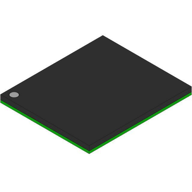
Available in 165-ball FBGA package (15 x 17 x 1.4 mm)
■
Offered in both Pb-free and non Pb-free packages
■
Variable drive HSTL output buffers
■
JTAG 1149.1 compatible test access port
■
Phase Locked Loop (PLL) for accurate data placement
CY7C1610KV18 – 16M x 8
CY7C1625KV18 – 16M x 9
CY7C1612KV18 – 8M x 18
CY7C1614KV18 – 4M x 36
Functional Description
The CY7C1610KV18, CY7C1625KV18, CY7C1612KV18, and
CY7C1614KV18 are 1.8V Synchronous Pipelined SRAMs,
equipped with QDR-II architecture. QDR-II architecture consists
of two separate ports to access the memory array. The read port
has dedicated data outputs to support read operations and the
write port has dedicated data inputs to support write operations.
QDR-II architecture has separate data inputs and data outputs
to completely eliminate the need to turn around the data bus that
exists with common IO devices. Each port is accessed through
a common address bus. The read address is latched on the
rising edge of the K clock and the write address is latched on the
rising edge of the K clock. Accesses to the QDR-II read and write
ports are completely independent of one another. To maximize
data throughput, both read and write ports are equipped with
DDR interfaces. Each address location is associated with two
8-bit words (CY7C1610KV18), 9-bit words (CY7C1625KV18),
18-bit
words
(CY7C1612KV18),
or
36-bit
words
(CY7C1614KV18) that burst sequentially into or out of the
device. Because data is transferred into and out of the device on
every rising edge of input clocks (K and K and C and C), memory
bandwidth is maximized while simplifying system design by
eliminating bus turn arounds.
Port selects for each port enable depth expansion. Port selects
allow each port to operate independently.
All synchronous inputs pass through input registers controlled by
the K or K input clocks. All data outputs pass through output
registers controlled by the C or C (or K or K in a single clock
domain) input clocks. Writes are conducted with on-chip
synchronous self-timed write circuitry.
Selection Guide
Parameter
333 MHz
300 MHz
250 MHz
200 MHz
Unit
333
300
250
200
MHz
x8/x9
850
780
680
580
mA
x18
870
810
700
590
x36
1060
980
850
710
Maximum Operating Frequency
Maximum Operating Current
Cypress Semiconductor Corporation
Document #: 001-16238 Rev. **
•
198 Champion Court
•
San Jose, CA 95134-1709
•
408-943-2600
Revised June 21, 2007
�CY7C1610KV18, CY7C1625KV18
CY7C1612KV18, CY7C1614KV18
ADVANCE
INFORMATION
Overview
Figure 1. Logic Block Diagram (CY7C1610KV18)
Block Diagram
K
K
CLK
Gen.
DOFF
Address
Register
Read Add. Decode
23
Write
Reg
8M x 8 Array
Address
Register
Write
Reg
8M x 8 Array
A(22:0)
8
Write Add. Decode
D[7:0]
23
A(22:0)
RPS
Control
Logic
C
C
Read Data Reg.
CQ
CQ
16
VREF
WPS
NWS[1:0]
Reg.
8
Control
Logic
Reg.
8
Reg.
8
8 Q
[7:0]
8
Figure 2. Logic Block Diagram (CY7C1625KV18)
Block Diagram
K
K
CLK
Gen.
DOFF
VREF
WPS
BWS[0]
Address
Register
Read Add. Decode
23
Write
Reg
8M x 9 Array
Address
Register
Write
Reg
8M x 9 Array
A(22:0)
9
Write Add. Decode
D[8:0]
23
A(22:0)
RPS
Control
Logic
C
C
Read Data Reg.
CQ
CQ
18
Control
Logic
9
Reg.
9
Reg.
9
Document #: 001-16238 Rev. **
Reg.
9
9 Q
[8:0]
Page 2 of 8
�CY7C1610KV18, CY7C1625KV18
CY7C1612KV18, CY7C1614KV18
ADVANCE
INFORMATION
Figure 3. Logic Block Diagram (CY7C1612KV18)
Block Diagram
K
K
CLK
Gen.
DOFF
Address
Register
Read Add. Decode
22
Write
Reg
4M x 18 Array
Address
Register
Write
Reg
4M x 18 Array
A(21:0)
18
Write Add. Decode
D[17:0]
22
RPS
Control
Logic
C
C
Read Data Reg.
36
VREF
WPS
BWS[1:0]
CQ
CQ
18
Reg.
Control
Logic
A(21:0)
18
Reg.
18
18
Reg.
Q[17:0]
18
Figure 4. Logic Block Diagram (CY7C1614KV18)
Block Diagram
K
K
CLK
Gen.
DOFF
VREF
WPS
BWS[3:0]
Address
Register
Read Add. Decode
21
Write
Reg
2M x 36 Array
Address
Register
Write
Reg
2M x 36 Array
A(20:0)
36
Write Add. Decode
D[35:0]
21
RPS
Control
Logic
C
C
Read Data Reg.
72
Control
Logic
Reg.
Reg.
36
Reg.
36
36
Document #: 001-16238 Rev. **
CQ
CQ
36
36
A(20:0)
Q[35:0]
Page 3 of 8
�CY7C1610KV18, CY7C1625KV18
CY7C1612KV18, CY7C1614KV18
ADVANCE
INFORMATION
Pin Configurations
165-Ball FBGA (15 x 17 x 1.4 mm) Pinout
Table 1. CY7C1610KV18 (16M x 8)[1]
A
B
C
D
E
F
G
H
J
K
L
M
N
P
R
1
2
3
4
5
6
7
8
9
CQ
NC
NC
NC
NC
D4
NC
10
11
A
A
NWS1
NC/288M
A
NC
WPS
A
K
NC
RPS
A
A
A
CQ
NC
NC
Q3
VSS
VSS
VSS
VSS
NC
NC
NC
NC
NC
D3
NC
NC
Q4
VDDQ
NC
NC
NC
NC
DOFF
NC
D5
VREF
NC
Q5
VDDQ
NC
NC
NC
NC
Q6
NC
NC
VSS
K
A
VSS
NWS0
A
VSS
VSS
VSS
VSS
VDDQ
NC
D2
Q2
VDDQ
VDD
VSS
VSS
VSS
VSS
VDDQ
VDDQ
VDDQ
NC
NC
VDDQ
NC
NC
VDD
VDD
VDD
VDD
VDD
VDD
VDD
VDDQ
VDDQ
VDDQ
VDDQ
NC
VREF
Q1
NC
NC
ZQ
D1
NC
VDDQ
VDD
VSS
VDD
VDDQ
NC
NC
NC
D6
VDDQ
VSS
VSS
VSS
VDDQ
NC
NC
Q0
NC
D7
NC
NC
VSS
VSS
VSS
A
VSS
A
VSS
A
VSS
VSS
NC
NC
NC
NC
D0
NC
NC
NC
Q7
A
A
C
A
A
NC
NC
NC
TDO
TCK
A
A
A
C
A
A
A
TMS
TDI
NC
A
Table 2. CY7C1625KV18 (16M x 9)[1]
A
B
C
D
E
F
G
H
J
K
L
M
N
P
R
1
2
3
4
5
6
7
8
9
10
11
CQ
A
A
WPS
NC
K
A
RPS
A
A
CQ
NC
NC
NC
A
NC/288M
K
BWS0
A
NC
NC
Q4
NC
NC
NC
D5
NC
NC
VSS
VSS
A
VSS
A
VSS
A
VSS
VSS
VSS
NC
NC
NC
NC
D4
NC
NC
NC
Q5
VDDQ
VSS
VSS
VSS
VDDQ
NC
D3
Q3
NC
NC
NC
VDDQ
VDD
VSS
VDD
VDDQ
NC
NC
NC
NC
DOFF
NC
D6
VREF
NC
Q6
VDDQ
NC
VDDQ
VDDQ
VDDQ
VDD
VDD
VDD
VSS
VSS
VSS
VDD
VDD
VDD
VDDQ
VDDQ
VDDQ
NC
VDDQ
NC
NC
VREF
Q2
NC
ZQ
D2
NC
NC
NC
VDDQ
VDD
VSS
VDD
VDDQ
NC
NC
NC
NC
Q7
D7
VDDQ
VSS
VSS
VSS
VDDQ
NC
NC
Q1
NC
NC
NC
D8
NC
NC
VSS
VSS
VSS
A
VSS
A
VSS
A
VSS
VSS
NC
NC
NC
NC
D1
NC
NC
NC
Q8
A
A
C
A
A
NC
D0
Q0
TDO
TCK
A
A
A
C
A
A
A
TMS
TDI
Note
1. NC/288M is not connected to the die and can be tied to any voltage level.
Document #: 001-16238 Rev. **
Page 4 of 8
�ADVANCE
INFORMATION
CY7C1610KV18, CY7C1625KV18
CY7C1612KV18, CY7C1614KV18
165-Ball FBGA (15 x 17 x 1.4 mm) Pinout
Table 3. CY7C1612KV18 (8M x 18)[1]
A
B
C
D
E
F
G
H
J
K
L
M
N
P
R
1
2
3
CQ
NC
A
A
4
Q9
D9
WPS
A
NC
NC
NC
D11
D10
Q10
VSS
VSS
5
6
7
BWS1
NC
K
K
NC/288M
8
9
10
11
A
CQ
BWS0
RPS
A
A
NC
NC
Q8
A
VSS
A
VSS
A
VSS
VSS
VSS
NC
Q7
NC
D8
D7
NC
NC
NC
Q11
VDDQ
VSS
VSS
VSS
VDDQ
NC
D6
Q6
NC
Q12
D12
VDDQ
VDD
VSS
VDD
VDDQ
NC
NC
Q5
NC
DOFF
NC
D13
VREF
NC
Q13
VDDQ
D14
VDDQ
VDDQ
VDDQ
VDD
VDD
VDD
VSS
VSS
VSS
VDD
VDD
VDD
VDDQ
VDDQ
VDDQ
NC
VDDQ
NC
NC
VREF
Q4
D5
ZQ
D4
NC
NC
Q14
VDDQ
VDD
VSS
VDD
VDDQ
NC
D3
Q3
NC
Q15
D15
VDDQ
VSS
VSS
VSS
VDDQ
NC
NC
Q2
NC
NC
NC
D17
D16
Q16
VSS
VSS
VSS
A
VSS
A
VSS
A
VSS
VSS
NC
NC
Q1
NC
D2
D1
NC
NC
Q17
A
A
C
A
A
NC
D0
Q0
TDO
TCK
A
A
A
C
A
A
A
TMS
TDI
4
5
6
7
8
9
10
11
RPS
A
A
A
CQ
D17
Q17
Q8
D16
Q7
D15
D8
D7
Table 4. CY7C1614KV18 (4M x 36)[1]
A
B
C
D
E
F
G
H
J
K
L
M
N
P
R
1
2
3
CQ
Q27
NC/288M
A
Q18
D18
D27
D28
Q28
D20
D19
Q19
Q29
D29
Q20
VDDQ
VSS
VSS
Q30
Q21
D21
VDDQ
VDD
VSS
D30
DOFF
D31
D22
VREF
Q31
Q22
VDDQ
D23
VDDQ
VDDQ
VDDQ
VDD
VDD
VDD
VSS
VSS
VSS
VDD
VDD
VDD
Q32
D32
Q23
VDDQ
VDD
VSS
Q33
Q24
D24
VDDQ
VSS
D33
D34
Q34
D26
D25
Q25
VSS
VSS
VSS
A
Q35
D35
Q26
A
A
TDO
TCK
A
A
A
Document #: 001-16238 Rev. **
WPS
A
VSS
VSS
BWS2
K
BWS1
BWS3
A
K
A
VSS
BWS0
A
VSS
VSS
VSS
VSS
Q16
VSS
VDDQ
Q15
D6
Q6
VDD
VDDQ
Q14
VDDQ
VDDQ
VDDQ
D14
Q13
VDDQ
D12
D13
VREF
Q4
Q5
D5
ZQ
D4
VDD
VDDQ
Q12
D3
Q3
VSS
VSS
VDDQ
D11
Q11
Q2
VSS
A
VSS
A
VSS
VSS
D10
Q10
Q1
D9
D2
D1
C
A
A
Q9
D0
Q0
C
A
A
A
TMS
TDI
Page 5 of 8
�ADVANCE
INFORMATION
CY7C1610KV18, CY7C1625KV18
CY7C1612KV18, CY7C1614KV18
Ordering Information
Not all of the speed, package and temperature ranges are available. Contact your local sales representative or visit www.cypress.com
for actual products offered.
Table 5. Ordering Information
Speed
(MHz)
333
Ordering Code
CY7C1610KV18-333BZC
Package
Diagram
Package Type
51-85195 165-Ball Fine Pitch Ball Grid Array (15 x 17 x 1.4 mm)
Operating
Range
Commercial
CY7C1625KV18-333BZC
CY7C1612KV18-333BZC
CY7C1614KV18-333BZC
CY7C1610KV18-333BZXC
51-85195 165-Ball Fine Pitch Ball Grid Array (15 x 17 x 1.4 mm) Pb-Free
CY7C1625KV18-333BZXC
CY7C1612KV18-333BZXC
CY7C1614KV18-333BZXC
CY7C1610KV18-333BZI
51-85195 165-Ball Fine Pitch Ball Grid Array (15 x 17 x 1.4 mm)
Industrial
CY7C1625KV18-333BZI
CY7C1612KV18-333BZI
CY7C1614KV18-333BZI
CY7C1610KV18-333BZXI
51-85195 165-Ball Fine Pitch Ball Grid Array (15 x 17 x 1.4 mm) Pb-Free
CY7C1625KV18-333BZXI
CY7C1612KV18-300BZXI
CY7C1614KV18-333BZXI
300
CY7C1610KV18-300BZC
51-85195 165-Ball Fine Pitch Ball Grid Array (15 x 17 x 1.4 mm)
Commercial
CY7C1625KV18-300BZC
CY7C1612KV18-300BZC
CY7C1614KV18-300BZC
CY7C1610KV18-300BZXC
51-85195 165-Ball Fine Pitch Ball Grid Array (15 x 17 x 1.4 mm) Pb-Free
CY7C1625KV18-300BZXC
CY7C1612KV18-300BZXC
CY7C1614KV18-300BZXC
CY7C1610KV18-300BZI
51-85195 165-Ball Fine Pitch Ball Grid Array (15 x 17 x 1.4 mm)
Industrial
CY7C1625KV18-300BZI
CY7C1612KV18-300BZI
CY7C1614KV18-300BZI
CY7C1610KV18-300BZXI
51-85195 165-Ball Fine Pitch Ball Grid Array (15 x 17 x 1.4 mm) Pb-Free
CY7C1625KV18-300BZXI
CY7C1612KV18-300BZXI
CY7C1614KV18-300BZXI
Document #: 001-16238 Rev. **
Page 6 of 8
�ADVANCE
INFORMATION
CY7C1610KV18, CY7C1625KV18
CY7C1612KV18, CY7C1614KV18
Table 5. Ordering Information (continued)
Speed
(MHz)
250
Ordering Code
CY7C1610KV18-250BZC
Package
Diagram
Package Type
51-85195 165-Ball Fine Pitch Ball Grid Array (15 x 17 x 1.4 mm)
Operating
Range
Commercial
CY7C1625KV18-250BZC
CY7C1612KV18-250BZC
CY7C1614KV18-250BZC
CY7C1610KV18-250BZXC
51-85195 165-Ball Fine Pitch Ball Grid Array (15 x 17 x 1.4 mm) Pb-Free
CY7C1625KV18-250BZXC
CY7C1612KV18-250BZXC
CY7C1614KV18-250BZXC
CY7C1610KV18-250BZI
51-85195 165-Ball Fine Pitch Ball Grid Array (15 x 17 x 1.4 mm)
Industrial
CY7C1625KV18-250BZI
CY7C1612KV18-250BZI
CY7C1614KV18-250BZI
CY7C1610KV18-250BZXI
51-85195 165-Ball Fine Pitch Ball Grid Array (15 x 17 x 1.4 mm) Pb-Free
CY7C1625KV18-250BZXI
CY7C1612KV18-250BZXI
CY7C1614KV18-250BZXI
200
CY7C1610KV18-200BZC
51-85195 165-Ball Fine Pitch Ball Grid Array (15 x 17 x 1.4 mm)
Commercial
CY7C1625KV18-200BZC
CY7C1612KV18-200BZC
CY7C1614KV18-200BZC
CY7C1610KV18-200BZXC
51-85195 165-Ball Fine Pitch Ball Grid Array (15 x 17 x 1.4 mm) Pb-Free
CY7C1625KV18-200BZXC
CY7C1612KV18-200BZXC
CY7C1614KV18-200BZXC
CY7C1610KV18-200BZI
51-85195 165-Ball Fine Pitch Ball Grid Array (15 x 17 x 1.4 mm)
Industrial
CY7C1625KV18-200BZI
CY7C1612KV18-200BZI
CY7C1614KV18-200BZI
CY7C1610KV18-200BZXI
51-85195 165-Ball Fine Pitch Ball Grid Array (15 x 17 x 1.4 mm) Pb-Free
CY7C1625KV18-200BZXI
CY7C1612KV18-200BZXI
CY7C1614KV18-200BZXI
Document #: 001-16238 Rev. **
Page 7 of 8
�ADVANCE
INFORMATION
CY7C1610KV18, CY7C1625KV18
CY7C1612KV18, CY7C1614KV18
Document History Page
Document Title: CY7C1610KV18/CY7C1625KV18/CY7C1612KV18/CY7C1614KV18 144-Mbit QDR™-II SRAM 2-Word
Burst Architecture
Document Number: 001-16238
REV.
ECN No.
Issue Date
Orig. of
Change
**
1184523
See ECN
VKN
Description of Change
New Data Sheet
© Cypress Semiconductor Corporation, 2007. The information contained herein is subject to change without notice. Cypress Semiconductor Corporation assumes no responsibility for the use of any
circuitry other than circuitry embodied in a Cypress product. Nor does it convey or imply any license under patent or other rights. Cypress products are not warranted nor intended to be used for medical,
life support, life saving, critical control or safety applications, unless pursuant to an express written agreement with Cypress. Furthermore, Cypress does not authorize its products for use as critical
components in life-support systems where a malfunction or failure may reasonably be expected to result in significant injury to the user. The inclusion of Cypress products in life-support systems
application implies that the manufacturer assumes all risk of such use and in doing so indemnifies Cypress against all charges.
Any Source Code (software and/or firmware) is owned by Cypress Semiconductor Corporation (Cypress) and is protected by and subject to worldwide patent protection (United States and foreign),
United States copyright laws and international treaty provisions. Cypress hereby grants to licensee a personal, non-exclusive, non-transferable license to copy, use, modify, create derivative works of,
and compile the Cypress Source Code and derivative works for the sole purpose of creating custom software and or firmware in support of licensee product to be used only in conjunction with a Cypress
integrated circuit as specified in the applicable agreement. Any reproduction, modification, translation, compilation, or representation of this Source Code except as specified above is prohibited without
the express written permission of Cypress.
Disclaimer: CYPRESS MAKES NO WARRANTY OF ANY KIND, EXPRESS OR IMPLIED, WITH REGARD TO THIS MATERIAL, INCLUDING, BUT NOT LIMITED TO, THE IMPLIED WARRANTIES
OF MERCHANTABILITY AND FITNESS FOR A PARTICULAR PURPOSE. Cypress reserves the right to make changes without further notice to the materials described herein. Cypress does not
assume any liability arising out of the application or use of any product or circuit described herein. Cypress does not authorize its products for use as critical components in life-support systems where
a malfunction or failure may reasonably be expected to result in significant injury to the user. The inclusion of Cypress’ product in a life-support systems application implies that the manufacturer
assumes all risk of such use and in doing so indemnifies Cypress against all charges.
Use may be limited by and subject to the applicable Cypress software license agreement.
Document #: 001-16238 Rev. **
Revised June 21, 2007
Page 8 of 8
QDR RAMs and Quad Data Rate RAMs comprise a new family of products developed by Cypress, IDT, NEC, Renesas, and Samsung. All product and company names mentioned in this document
are the trademarks of their respective holders.
�