1bCY7C185
CY7C185
8K x 8 Static RAM
Features
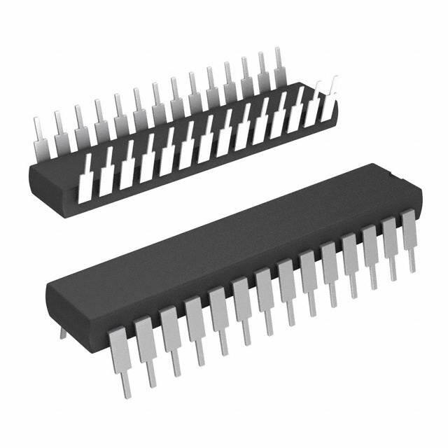
• High speed — 15 ns • Fast tDOE • Low active power — 715 mW • Low standby power — 85 mW • CMOS for optimum speed/power • Easy memory expansion with CE1, CE2 and OE features • TTL-compatible inputs and outputs • Automatic power-down when deselected • Available in non Pb-free 28-pin (300-Mil) Molded SOJ, 28-pin (300-Mil) Molded SOIC and both Pb-free and non Pb-free in 28-pin (300-Mil) Molded DIP
Functional Description[1]
The CY7C185 is a high-performance CMOS static RAM organized as 8192 words by 8 bits. Easy memory expansion is provided by an active LOW chip enable (CE1), an active HIGH chip enable (CE2), and active LOW output enable (OE) and tri-state drivers. This device has an automatic power-down feature (CE1 or CE2), reducing the power consumption by 70% when deselected. The CY7C185 is in a standard 300-mil-wide DIP, SOJ, or SOIC package. An active LOW write enable signal (WE) controls the writing/reading operation of the memory. When CE1 and WE inputs are both LOW and CE2 is HIGH, data on the eight data input/output pins (I/O0 through I/O7) is written into the memory location addressed by the address present on the address pins (A0 through A12). Reading the device is accomplished by selecting the device and enabling the outputs, CE1 and OE active LOW, CE2 active HIGH, while WE remains inactive or HIGH. Under these conditions, the contents of the location addressed by the information on address pins are present on the eight data input/output pins. The input/output pins remain in a high-impedance state unless the chip is selected, outputs are enabled, and write enable (WE) is HIGH. A die coat is used to insure alpha immunity.
Logic Block Diagram Pin Configurations
I/O0 INPUT BUFFER I/O1 A1 A2 A3 A4 A5 A6 A7 A8 ROW DECODER I/O2 I/O3 I/O4 I/O5 I/O6
CE1 CE2 WE OE NC A4 A5 A6 A7 A8 A9 A10 A11 A12 I/O0 I/O1 I/O2 GND
DIP/SOJ Top View
1 2 3 4 5 6 7 8 9 10 11 12 13 14 28 27 26 25 24 23 22 21 20 19 18 17 16 15 VCC WE CE2 A3 A2 A1 OE A0 CE1 I/O7 I/O6 I/O5 I/O4 I/O3
8K x 8 ARRAY
COLUMN DECODER
POWER DOWN
SENSE AMPS
I/O7
A10
A11
Selection Guide
Maximum Access Time (ns) Maximum Operating Current (mA) Maximum CMOS Standby Current (mA) -15 15 130 15 -20 20 110 15 -25 25 100 15 -35 35 100 15
Notes: 1. For guidelines on SRAM system design, please refer to the ‘System Design Guidelines’ Cypress application note, available on the internet at www.cypress.com.
A12
A0
A9
Cypress Semiconductor Corporation Document #: 38-05043 Rev. *B
•
198 Champion Court
•
San Jose, CA 95134-1709 • 408-943-2600 Revised July 24, 2006
[+] [+] Feedback
�CY7C185
Maximum Ratings
(Above which the useful life may be impaired. For user guidelines, not tested.) Storage Temperature ................................. –65°C to +150°C Ambient Temperature with Power Applied............................................. –55°C to +125°C Supply Voltage to Ground Potential ............... –0.5V to +7.0V DC Voltage Applied to Outputs in High Z State[2] ............................................ –0.5V to +7.0V DC Input Voltage[2] ......................................... –0.5V to +7.0V Output Current into Outputs (LOW)............................. 20 mA Static Discharge Voltage........................................... >2001V (per MIL-STD-883, Method 3015) Latch-Up Current .................................................... >200 mA
Operating Range
Range Commercial Industrial Ambient Temperature 0°C to +70°C –40°C to +85°C VCC 5V ± 10% 5V ± 10%
Electrical Characteristics Over the Operating Range
–15 Parameter VOH VOL VIH VIL IIX IOZ ICC ISB1 Description Output HIGH Voltage Output LOW Voltage Input HIGH Voltage Input LOW Voltage[2] Input Leakage Current GND ≤ VI ≤ VCC Test Conditions VCC = Min., IOH = –4.0 mA VCC = Min., IOL = 8.0 mA 2.2 –0.5 –5 –5 Min. 2.4 0.4 VCC + 0.3V 0.8 +5 +5 130 40 2.2 –0.5 –5 –5 Max. Min. 2.4 0.4 VCC + 0.3V 0.8 +5 +5 110 20 2.2 –0.5 –5 –5 –20 Max. 2.4 0.4 VCC + 0.3V 0.8 +5 +5 100 20 –25, -35 Min. Max. Unit V V V V µA µA mA mA
Output Leakage GND ≤ VI ≤ VCC, Current Output Disabled VCC Operating VCC = Max., Supply Current IOUT = 0 mA Automatic Power-Down Current Automatic Power-Down Current Max. VCC, CE1 ≥ VIH or CE2 ≤ VIL Min. Duty Cycle =100% Max. VCC, CE1 ≥ VCC – 0.3V, or CE2 ≤ 0.3V VIN ≥ VCC – 0.3V or VIN ≤ 0.3V
ISB2
15
15
15
mA
Capacitance[3]
Parameter CIN COUT Description Input Capacitance Output Capacitance Test Conditions TA = 25°C, f = 1 MHz, VCC = 5.0V Max. 7 7 Unit pF pF
Notes: 2. Minimum voltage is equal to –3.0V for pulse durations less than 30 ns. 3. Tested initially and after any design or process changes that may affect these parameters.
Document #: 38-05043 Rev. *B
Page 2 of 12
[+] [+] Feedback
�CY7C185
AC Test Loads and Waveforms
5V OUTPUT 30 pF INCLUDING JIG AND SCOPE R1 481 Ω 5V OUTPUT 5 pF INCLUDING JIGAND SCOPE R1 481 Ω 3.0V R2 255Ω GND 10% ALL INPUT PULSES 90% 90% 10% ≤ 5 ns
R2 255Ω
≤ 5 ns Equivalent to: OUTPUT
(a)
(b)
THÉVENIN EQUIVALENT 167Ω 1.73V
Switching Characteristics Over the Operating Range[4]
-15 Parameter Read Cycle tRC tAA tOHA tACE1 tACE2 tDOE tLZOE tHZOE tLZCE1 tLZCE2 tHZCE tPU tPD Write Cycle[7] tWC tSCE1 tSCE2 tAW tHA tSA tPWE tSD tHD tHZWE tLZWE Write Cycle Time CE1 LOW to Write End CE2 HIGH to Write End Address Set-up to Write End Address Hold from Write End Address Set-up to Write Start WE Pulse Width Data Set-up to Write End Data Hold from Write End WE LOW to High Z[5] WE HIGH to Low Z 3 15 12 12 12 0 0 12 8 0 7 5 20 15 15 15 0 0 15 10 0 7 5 25 20 20 20 0 0 15 10 0 7 5 35 20 20 25 0 0 20 12 0 8 ns ns ns ns ns ns ns ns ns ns ns Read Cycle Time Address to Data Valid Data Hold from Address Change CE1 LOW to Data Valid CE2 HIGH to Data Valid OE LOW to Data Valid OE LOW to Low Z OE HIGH to High Z[5] 3 3 7 0 15 0 20 CE1 LOW to Low Z[6] CE2 HIGH to Low Z CE1 HIGH to High CE2 LOW to High Z Z[5, 6] 3 7 5 3 8 0 20 3 15 15 8 3 8 5 3 10 0 20 15 15 5 20 20 9 3 10 5 3 10 20 20 5 25 25 12 3 10 25 25 5 35 35 15 35 35 ns ns ns ns ns ns ns ns ns ns ns ns ns Description Min. Max. Min. -20 Max. Min. -25 Max. Min. -35 Max. Unit
CE1 LOW to Power-Up CE2 to HIGH to Power-Up CE1 HIGH to Power-Down CE2 LOW to Power-Down
Notes: 4. Test conditions assume signal transition time of 5 ns or less, timing reference levels of 1.5V, input pulse levels of 0 to 3.0V, and output loading of the specified IOL/IOH and 30-pF load capacitance. 5. tHZOE, tHZCE, and tHZWE are specified with CL = 5 pF as in part (b) of AC Test Loads. Transition is measured ±500 mV from steady state voltage. 6. At any given temperature and voltage condition, tHZCE is less than tLZCE1 and tLZCE2 for any given device. 7. The internal write time of the memory is defined by the overlap of CE1 LOW, CE2 HIGH, and WE LOW. All 3 signals must be active to initiate a write and either signal can terminate a write by going HIGH. The data input set-up and hold timing should be referenced to the rising edge of the signal that terminates the write.
Document #: 38-05043 Rev. *B
Page 3 of 12
[+] [+] Feedback
�CY7C185
Switching Waveforms
Read Cycle No.1[8,9]
tRC ADDRESS tOHA DATA OUT PREVIOUS DATA VALID tAA DATA VALID
Read Cycle No.2[10,11]
CE1
tRC
CE2 OE OE
tACE
tDOE tLZOE HIGH IMPEDANCE tLZCE VCC SUPPLY CURRENT tPU 50%
tHZOE tHZCE DATA VALID tPD ICC 50% ISB HIGH IMPEDANCE
DATA OUT
Notes: 8. Device is continuously selected. OE, CE1 = VIL. CE2 = VIH. 9. WE is HIGH for read cycle. 10. Data I/O is High Z if OE = VIH, CE1 = VIH, WE = VIL, or CE2=VIL. 11. The internal write time of the memory is defined by the overlap of CE1 LOW, CE2 HIGH and WE LOW. CE1 and WE must be LOW and CE2 must be HIGH to initiate write. A write can be terminated by CE1 or WE going HIGH or CE2 going LOW. The data input set-up and hold timing should be referenced to the rising edge of the signal that terminates the write.
Document #: 38-05043 Rev. *B
Page 4 of 12
[+] [+] Feedback
�CY7C185
Switching Waveforms (continued)
Write Cycle No. 1 (WE Controlled)[9,11]
tWC ADDRESS CE1 tAW CE2 CE WE tSA tSCE2 tPWE tSCEI tHA
OE tSD DATA I/O NOTE 12 tHZOE DATA IN VALID tHD
Write Cycle No. 2 (CE Controlled)[11,12,13]
tWC ADDRESS CE1 tSA CE2 tAW WE tSD DATA I/O DATA IN VALID tHD tSCE2 tHA tSCE1
Notes: 12. During this period, the I/Os are in the output state and input signals should not be applied. 13. The minimum write cycle time for write cycle #3 (WE controlled, OE LOW) is the sum of tHZWE and tSD.
Document #: 38-05043 Rev. *B
Page 5 of 12
[+] [+] Feedback
�CY7C185
Switching Waveforms (continued)
Write Cycle No. 3(WE Controlled, OE LOW)[11,12,13,14]
tWC ADDRESS CE1 CE2 tSCE1 tSCE2 tAW tSA WE tSD DATA I/O NOTE 12 tHZWE
Note: 14. If CE1 goes HIGH or CE2 goes LOW simultaneously with WE HIGH, the output remains in a high-impedance state.
tHA
tHD
DATA IN VALID tLZWE
Document #: 38-05043 Rev. *B
Page 6 of 12
[+] [+] Feedback
�CY7C185
Typical DC and AC Characteristics
OUTPUT SOURCE CURRENT (mA) NORMALIZED SUPPLY CURRENT vs. SUPPLY VOLTAGE 1.4
SB
NORMALIZED SUPPLY CURRENT vs. AMBIENT TEMPERATURE 1.2
SB
OUTPUT SOURCE CURRENT vs. OUTPUT VOLTAGE 120 100 80 60 40 20 0 0.0 1.0 2.0 3.0 4.0 VCC =5.0V TA =25°C
1.2 1.0 0.8 0.6 0.4 0.2 0.0 4.0 4.5 5.0 I SB 5.5 6.0 I CC
1.0 0.8 0.6 0.4 0.2 0.0 –55 ISB 25 V CC=5.0V V IN=5.0V
NORMALIZED I,CC I
NORMALIZED I, I CC
I CC
125
SUPPLY VOLTAGE (V) NORMALIZED ACCESS TIME vs. SUPPLY VOLTAGE 1.4 NORMALIZED tAA NORMALIZED t AA 1.3 1.2 1.1 1.0 0.9 0.8 4.0 4.5 5.0 5.5 SUPPLY VOLTAGE (V) 6.0 TA =25°C 1.6 1.4 1.2 1.0
AMBIENT TEMPERATURE (°C) NORMALIZED ACCESS TIME vs. AMBIENT TEMPERATURE
OUTPUT VOLTAGE (V) OUTPUT SINK CURRENT vs. OUTPUT VOLTAGE 140 120 100 80 60 40 20 0 0.0 1.0 2.0 3.0 OUTPUT VOLTAGE (V) 4.0 VCC =5.0V TA =25°C
VCC =5.0V 0.8 0.6 –55
25
125
AMBIENT TEMPERATURE (°C)
TYPICAL POWER-ON CURRENT vs. SUPPLY VOLTAGE 3.0 NORMALIZED I PO DELTA tAA (ns) 2.5 2.0 1.5 1.0 0.5 0.0 0.0 1.0 2.0 3.0 4.0 5.0 30.0
TYPICAL ACCESS TIME CHANGE vs. OUTPUT LOADING 1.25 NORMALIZED I CC
OUTPUT SINK CURRENT (mA)
NORMALIZED I CC vs. CYCLE TIME VCC =5.0V TA =25°C VCC =0.5V 1.00
25.0 20.0 15.0 10.0 5.0 0.0 0 200 400 VCC =4.5V TA =25°C
0.75
600
800 1000
0.50 10
20
30
40
SUPPLY VOLTAGE (V)
CAPACITANCE (pF)
CYCLE FREQUENCY (MHz)
Document #: 38-05043 Rev. *B
Page 7 of 12
[+] [+] Feedback
�CY7C185
Truth Table
CE1 H X L L L CE2 X L H H H WE X X H L H OE X X L X H High Z High Z Data Out Data In High Z Input/Output Mode Deselect/Power-Down Deselect/Power-Down Read Write Deselect
Address Designators
Address Name A4 A5 A6 A7 A8 A9 A10 A11 A12 A0 A1 A2 A3 Address Function X3 X4 X5 X6 X7 Y1 Y4 Y3 Y0 Y2 X0 X1 X2 Pin Number 2 3 4 5 6 7 8 9 10 21 23 24 25
Ordering Information
Speed (ns) 15 20 Ordering Code CY7C185-15VC CY7C185-15VI CY7C185-20PC CY7C185-20PXC CY7C185-20VC 25 35 CY7C185-25PC CY7C185-25VC CY7C185-35PC CY7C185-35SC 51-85031 51-85014 51-85031 51-85014 51-85026 51-85014 Package Name 51-85031 Package Type 28-pin (300-Mil) Molded SOJ 28-pin (300-Mil) Molded SOJ 28-pin (300-Mil) Molded DIP 28-pin (300-Mil) Molded DIP (Pb-free) 28-pin (300-Mil) Molded SOJ 28-pin (300-Mil) Molded DIP 28-pin (300-Mil) Molded SOJ 28-pin (300-Mil) Molded DIP 28-pin (300-Mil) Molded SOIC Commercial Commercial Operating Range Commercial Industrial Commercial
Document #: 38-05043 Rev. *B
Page 8 of 12
[+] [+] Feedback
�CY7C185
Package Diagrams
28-pin (300-Mil) PDIP (51-85014)
SEE LEAD END OPTION
14
1
DIMENSIONS IN INCHES [MM] MIN. MAX.
0.260[6.60] 0.295[7.49]
REFERENCE JEDEC MO-095 PACKAGE WEIGHT: 2.15 gms
15
28
0.030[0.76] 0.080[2.03]
SEATING PLANE 1.345[34.16] 1.385[35.18]
0.290[7.36] 0.325[8.25] 0.120[3.05] 0.140[3.55] 0.009[0.23] 0.012[0.30]
0.140[3.55] 0.190[4.82] 0.115[2.92] 0.160[4.06] 0.055[1.39] 0.065[1.65] 0.015[0.38] 0.020[0.50]
3° MIN.
0.015[0.38] 0.060[1.52] 0.090[2.28] 0.110[2.79]
0.310[7.87] 0.385[9.78] SEE LEAD END OPTION
LEAD END OPTION (LEAD #1, 14, 15 & 28)
51-85014-*D
Document #: 38-05043 Rev. *B
Page 9 of 12
[+] [+] Feedback
�CY7C185
Package Diagrams (continued)
28-pin (300-Mil) Molded SOIC (51-85026)
NOTE :
PIN 1 ID
1. JEDEC STD REF MO-119 2. BODY LENGTH DIMENSION DOES NOT INCLUDE MOLD PROTRUSION/END FLASH,BUT DOES INCLUDE MOLD MISMATCH AND ARE MEASURED AT THE MOLD PARTING LINE. MOLD PROTRUSION/END FLASH SHALL NOT EXCEED 0.010 in (0.254 mm) PER SIDE 3. DIMENSIONS IN INCHES MIN. MAX.
14
1
0.291[7.39] 0.300[7.62]
4. PACKAGE WEIGHT 0.85gms
*
0.394[10.01] 0.419[10.64]
15
28
0.026[0.66] 0.032[0.81]
PART # S28.3 STANDARD PKG. SZ28.3 LEAD FREE PKG.
0.697[17.70] 0.713[18.11]
SEATING PLANE
0.092[2.33] 0.105[2.67] 0.004[0.10] 0.013[0.33] 0.050[1.27] TYP.
51-85026-*D
0.004[0.10] 0.0118[0.30]
*
0.019[0.48]
0.015[0.38] 0.050[1.27]
0.0091[0.23] 0.0125[3.17]
*
Document #: 38-05043 Rev. *B
Page 10 of 12
[+] [+] Feedback
�CY7C185
Package Diagrams (continued)
28-pin (300-Mil) Molded SOJ (51-85031)
NOTE : 1. JEDEC STD REF MO088 2. BODY LENGTH DIMENSION DOES NOT INCLUDE MOLD PROTRUSION/END FLASH MOLD PROTRUSION/END FLASH SHALL NOT EXCEED 0.006 in (0.152 mm) PER SIDE 3. DIMENSIONS IN INCHES MIN. MAX.
PIN 1 ID
14 1
DETAIL A EXTERNAL LEAD DESIGN
0.291 0.300
0.330 0.350 0.013 0.019
OPTION 1 OPTION 2
0.026 0.032 0.014 0.020
15
28
0.697 0.713 0.120 0.140 0.050 TYP.
SEATING PLANE
0.007 0.013
0.004
A
0.025 MIN.
0.262 0.272
51-85031-*C
All product and company names mentioned in this document may be the trademarks of their respective holders.
Document #: 38-05043 Rev. *B
Page 11 of 12
© Cypress Semiconductor Corporation, 2006. The information contained herein is subject to change without notice. Cypress Semiconductor Corporation assumes no responsibility for the use of any circuitry other than circuitry embodied in a Cypress product. Nor does it convey or imply any license under patent or other rights. Cypress products are not warranted nor intended to be used for medical, life support, life saving, critical control or safety applications, unless pursuant to an express written agreement with Cypress. Furthermore, Cypress does not authorize its products for use as critical components in life-support systems where a malfunction or failure may reasonably be expected to result in significant injury to the user. The inclusion of Cypress products in life-support systems application implies that the manufacturer assumes all risk of such use and in doing so indemnifies Cypress against all charges.
[+] [+] Feedback
�CY7C185
Document History Page
Document Title: CY7C185 8K x 8 Static RAM Document Number: 38-05043 REV. ** *A *B ECN NO. 107145 116470 486744 Issue Date 09/10/01 09/16/02 See ECN Orig. of Change SZV CEA NXR Description of Change Change from Spec number: 38-00037 to 38-05043 Add applications foot note to data sheet Changed Low standby power from 220mW to 85mW Changed the description of IIX from Input Load Current to Input Leakage Current in DC Electrical Characteristics table Removed IOS parameter from DC Electrical Characteristics table Updated the Ordering Information table
Document #: 38-05043 Rev. *B
Page 12 of 12
[+] [+] Feedback
�


 工商网监
湘ICP备2023018690号
工商网监
湘ICP备2023018690号
