CY7C187
64K x 1 Static RAM
Features
Functional Description
■
High Speed
❐ 25 ns
■
CMOS for Optimum Speed and Power
■
Low Active Power
❐ 385 mW
The CY7C187 is a high performance CMOS static RAM
organized as 65,536 words x 1 bit. Easy memory expansion is
provided by an active LOW Chip Enable (CE) and tristate drivers.
The CY7C187 has an automatic power down feature, reducing
the power consumption by 56% when deselected.
Writing to the device is possible when the Chip Enable (CE) and
Write Enable (WE) inputs are both LOW. Data on the input pin
(DIN) is written into the memory location specified on the address
pins (A0 through A15).
■
Low Standby Power
❐ 110 mW
■
TTL Compatible Inputs and Outputs
■
Automatic Power Down when Deselected
■
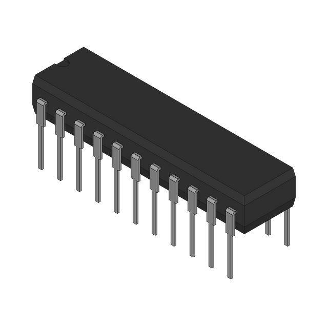
Available in Pb-free 22-Pin (300-Mil) Molded DIP
Reading the device is possible by taking the Chip Enable (CE)
LOW, while Write Enable (WE) remains HIGH. Under these
conditions, the contents of the memory location specified on the
address pin appears on the data output (DOUT) pin.
The output pin stays in high impedance state when CE is HIGH
or WE is LOW.
The CY7C187 uses a die coat to insure alpha immunity.
Logic Block Diagram
DI
ROW DECODER
A12
A13
A14
A15
A0
A1
A2
A3
16K x 1
ARRAY
SENSE AMPS
INPUT BUFFER
DO
CE
COLUMN DECODER
POWER
DOWN
A4
A5
A6
A7
A8
A9
A10
A11
WE
Cypress Semiconductor Corporation
Document #: 38-05044 Rev. *B
•
198 Champion Court
•
San Jose, CA 95134-1709
•
408-943-2600
Revised August 19, 2009
[+] Feedback
�CY7C187
Selection Guide
Description
Maximum Access Time (ns)
Maximum Operating Current (mA)
Maximum CMOS Standby Current (mA)
-25
25
70
20
-35
35
70
20
Pin Configuration
Figure 1. Pin Diagram DIP - Top View
A0
A1
A2
A3
A4
A5
A6
A7
DOUT
WE
GND
Document #: 38-05044 Rev. *B
1
2
3
4
5
6
7
8
9
10
11
22
21
20
19
18
17
16
15
14
13
12
VCC
A15
A14
A13
A12
A11
A10
A9
A8
DIN
CE
Page 2 of 9
[+] Feedback
�CY7C187
DC Input Voltage[1] .........................................–0.5V to +7.0V
Maximum Ratings
Exceeding the maximum ratings may impair the useful life of the
device. User guidelines are not tested.
Storage Temperature ................................. –65°C to +150°C
Output Current into Outputs (LOW)............................. 20 mA
Static Discharge Voltage............................................ >2001V
(per MIL–STD–883, Method 3015)
Latch Up Current ..................................................... >200 mA
Ambient Temperature with
Power Applied ............................................ –55°C to +125°C
Operating Range
Supply Voltage to Ground Potential
(Pin 22 to Pin 11) ............................................–0.5V to +7.0V
Range
VCC
DC Voltage Applied to Outputs
in High Z State[1] .............................................–0.5V to +7.0V
Ambient
Temperature
Commercial
0°C to +70°C
5V ± 10%
Electrical Characteristics Over the Operating Range
Parameter
Description
-25 and -35
Test Conditions
VOH
Output HIGH Voltage
VCC = Min., IOH = –4.0 mA
VOL
Output LOW Voltage
VCC = Min., IOL =12.0 mA
VIH
Input HIGH Voltage
Min
Max
Unit
2.4
Voltage[1]
V
0.4
V
2.2
VCC
V
–0.5
0.8
V
VIL
Input LOW
IIX
Input Leakage Current
GND < VI < VCC
–5
+5
μA
IOZ
Output Leakage Current
GND < VO < VCC,
Output Disabled
–5
+5
μA
ICC
VCC Operating Supply Current
VCC = Max.,
IOUT = 0 mA
70
mA
ISB1
Automatic CE Power Down
Current[3]
Max. VCC, CE ≥ VIH
20
mA
ISB2
Automatic C Power Down
Current
Max. VCC, CE ≥ VCC – 0.3V,
VIN ≥ VCC – 0.3V
or VIN ≤ 0.3V
20
mA
Capacitance[4]
Parameter
Description
CIN
Input Capacitance
COUT
Output Capacitance
Test Conditions
TA = 25°C, f = 1 MHz,
VCC = 5.0V
Max
Unit
10
pF
10
pF
Figure 2. AC Test Loads and Waveforms
R1 329 Ω
ALL INPUT PULSES
R1 329 Ω
5V
OUTPUT
3.0V
5V
OUTPUT
R2 202 Ω
30 pF
INCLUDING
JIG AND
SCOPE
(a)
R2 202 Ω
5 pF
INCLUDING
JIG AND
SCOPE
GND
10%
90%
≤ 5 ns
90%
10%
≤ 5 ns
C187–5
(b)
C187–4
Equivalent to:
THÉ VENIN EQUIVALENT
125Ω
OUTPUT
1.90V
Notes
1. VIL (min.) = –3.0V for pulse durations less than 30 ns.
2. Not more than one output should be shorted at one time. Duration of the short circuit should not exceed 30 seconds.
3. A pull up resistor to VCC on the CE input is required to keep the device deselected during VCC power up, otherwise ISB exceeds values given.
4. Tested initially and after any design or process changes that may affect these parameters.
Document #: 38-05044 Rev. *B
Page 3 of 9
[+] Feedback
�CY7C187
Switching Characteristics Over the Operating Range[5]
Parameter
-25
Description
Min
-35
Max
Min
Max
Unit
Read Cycle
tRC
Read Cycle Time
tAA
Address to Data Valid
25
tOHA
Output Hold from Address Change
tACE
CE LOW to Data Valid
CE LOW to Low Z
tHZCE
CE HIGH to High Z[6,7]
tPU
CE LOW to Power Up
tPD
Write
5
5
5
5
0
ns
ns
15
0
20
ns
ns
35
10
CE HIGH to Power Down
ns
35
25
[6]
tLZCE
35
25
ns
ns
20
ns
Cycle[8]
tWC
Write Cycle Time
20
25
ns
tSCE
CE LOW to Write End
20
25
ns
tAW
Address Setup to Write End
20
25
ns
tHA
Address Hold from Write End
0
0
ns
tSA
Address Setup to Write Start
0
0
ns
tPWE
WE Pulse Width
15
20
ns
tSD
Data Setup to Write End
10
15
ns
tHD
Data Hold from Write End
0
0
ns
tLZWE
WE HIGH to Low Z
5
5
ns
tHZWE
WE LOW to High
Z[7]
7
10
ns
Switching Waveforms
Figure 3. Read Cycle No. 1[9, 10]
tRC
ADDRESS
tOHA
DATA OUT
PREVIOUS DATA VALID
tAA
DATA VALID
Notes
5. Test conditions assume signal transition time of 5 ns or less, timing reference levels of 1.5V, input pulse levels of 0 to 3.0V, and output loading of the specified IOL/IOH
and 30 pF load capacitance.
6. At any temperature and voltage condition, tHZCE is less than tLZCE for any device.
7. tHZCE and tHZWE are specified with CL = 5 pF as in part (b) of AC Test Loads and Waveforms on page 3. Transition is measured ±500 mV from steady-state voltage.
8. The internal write time of the memory is defined by the overlap of CE LOW and WE LOW. Both signals must be LOW to initiate a write and either signal can terminate
a write by going HIGH. The data input setup and hold timing should be referenced to the rising edge of the signal that terminates the write.
9. WE is HIGH for read cycle.
10. Device is continuously selected, CE = VIL.
Document #: 38-05044 Rev. *B
Page 4 of 9
[+] Feedback
�CY7C187
Figure 4. Read Cycle No. 2[9, 11]
tRC
CE
tACE
tHZCE
tLZCE
DATA OUT
HIGH IMPEDANCE
VCC
SUPPLY
CURRENT
HIGH
IMPEDANCE
DATA VALID
tPD
tPU
ICC
50%
50%
ISB
Figure 5. Write Cycle No. 1(WE Controlled)[11]
tWC
ADDRESS
tSCE
CE
tSA
tAW
tHA
tPWE
WE
tSD
DATA IN
tHD
DATA VALID
tHZWE
tLZWE
HIGH IMPEDANCE
DATA OUT
DATA UNDEFINED
Figure 6. Write Cycle No. 2(CE Controlled)[11,12]
tWC
ADDRESS
tSA
tSCE
CE
tAW
tHA
tPWE
WE
tSD
DATA IN
tHD
DATA VALID
DATA OUT
HIGH IMPEDANCE
Notes
11. Address valid prior to or coincident with CE transition LOW.
12. If CE goes HIGH simultaneously with WE HIGH, the output remains in a high impedance state
Document #: 38-05044 Rev. *B
Page 5 of 9
[+] Feedback
�CY7C187
NORMALIZED SUPPLY CURRENT
vs. AMBIENT TEMPERATURE
NORMALIZED SUPPLY CURRENT
vs. SUPPLY VOLTAGE
1.2
NORMALIZED I CC, I SB
1.2
I CC
0.8
0.6
0.4
0.0
4.0
4.5
5.0
I CC
0.8
0.6
0.4
VCC =5.0V
VIN =5.0V
0.2
ISB
0.2
1.0
5.5
ISB
0.0
–55
6.0
NORMALIZED ACCESS TIME
vs. AMBIENT TEMPERATURE
NORMALIZED ACCESS TIME
vs. SUPPLY VOLTAGE
1.6
1.3
NORMALIZED t AA
NORMALIZED t AA
1.4
1.2
1.1
TA =25°C
1.0
1.4
1.2
1.0
VCC =5.0V
0.8
0.9
0.8
4.0
4.5
5.0
5.5
0.6
–55
6.0
25
AMBIENT TEMPERATURE (°C)
TYPICAL POWER-ON CURRENT
vs. SUPPLY VOLTAGE
TYPICAL ACCESS TIME CHANGE
vs. OUTPUT LOADING
NORMALIZED t AA (ns)
2.5
2.0
1.5
1.0
1.0
2.0
3.0
4.0
SUPPLY VOLTAGE(V)
Document #: 38-05044 Rev. *B
100
80
VCC =5.0V
TA =25°C
60
40
20
0
0.0
5.0
2.0
3.0
4.0
140
120
100
VCC =5.0V
TA =25°C
80
60
40
20
1.0
2.0
3.0
4.0
OUTPUT VOLTAGE (V)
NORMALIZED I CC vs.CYCLE TIME
1.25
25.0
20.0
15.0
10.0
0.0
1.0
OUTPUT SINK CURRENT
vs. OUTPUT VOLTAGE
0
0.0
30.0
VCC =4.5V
TA =25°C
5.0
0.5
0.0
0.0
120
OUTPUT VOLTAGE (V)
125
SUPPLY VOLTAGE (V)
3.0
PO
125
OUTPUT SOURCE CURRENT
vs. OUTPUT VOLTAGE
AMBIENT TEMPERATURE (°C)
SUPPLY VOLTAGE(V)
NORMALIZED I
25
OUTPUT SINK CURRENT (mA)
1.0
0
200
400
600
800 1000
CAPACITANCE (pF)
NORMALIZED I CC
NORMALIZED I CC, ISB
1.4
OUTPUT SOURCE CURRENT (mA)
Typical DC and AC Characteristics
VCC =5.0V
TA =25°C
VCC =0.5V
1.00
0.75
0.50
10
20
30
40
CYCLE FREQUENCY (MHz)
Page 6 of 9
[+] Feedback
�CY7C187
Address Designators
Address Name
Address Function
Pin Number
A0
X3
1
A1
X4
2
A2
X5
3
A3
X6
4
A4
X7
5
A5
Y7
6
A6
Y6
7
A7
Y2
8
A8
Y3
14
A9
Y1
15
A10
Y0
16
A11
Y4
17
A12
Y5
18
A13
X0
19
A14
X1
20
A15
X2
21
Truth Table
CE
WE
H
X
High Z
Deselect/Power Down
L
H
Data Out
Read
L
L
Data In
Write
Document #: 38-05044 Rev. *B
Input/Output
Mode
Page 7 of 9
[+] Feedback
�CY7C187
Ordering Information
Speed (ns)
Ordering Code
Package Diagram
Package Type
25
CY7C187-25PXC
51-85012
22-Pin (300-Mil) Molded DIP
35
CY7C187-35PXC
51-85012
22-Pin (300-Mil) Molded DIP
Operating Range
Commercial
Contact your local Cypress sales representatives for the availability of parts
Package Diagram
Figure 7. 22-Pin (300 Mil) PDIP
11
1
DIMENSIONS IN INCHES MIN.
MAX.
0.250
0.270
12
22
0.030
0.065
1.070
1.120
SEATING PLANE
0.120
0.140
0.140
0.190
0.115
0.160
0.015
0.060
0.090
0.110
0.280
0.325
0.055
0.065
0.015
0.020
0.009
0.012
3° MIN.
0.310
0.385
51-85012-*A
Document #: 38-05044 Rev. *B
Page 8 of 9
[+] Feedback
�CY7C187
Document History Page
Document Title: CY7C187 64K x 1 Static RAM
Document Number: 38-05044
Rev.
ECN No.
Orig. of
Change
Submission Description of Change
Date
**
107146
SZV
09/10/01
Change from Spec number: 38-00038 to 38-05044
*A
486744
NXR
See ECN
Removed 20 ns speed bin
Changed Low standby power from 220mW to 110mW
Changed the description of IIX from Input Load Current to Input Leakage
Current in DC Electrical Characteristics table
Updated the Ordering Information Table
*B
2753814
NXR
08/19/09
Removed SOJ package from product offering
Updated the Ordering Information Table
Sales, Solutions, and Legal Information
Worldwide Sales and Design Support
Cypress maintains a worldwide network of offices, solution centers, manufacturer’s representatives, and distributors. To find the office
closest to you, visit us at cypress.com/sales.
Products
PSoC
Clocks & Buffers
psoc.cypress.com
clocks.cypress.com
Wireless
wireless.cypress.com
Memories
memory.cypress.com
Image Sensors
image.cypress.com
© Cypress Semiconductor Corporation, 2001-2009. The information contained herein is subject to change without notice. Cypress Semiconductor Corporation assumes no responsibility for the use
of any circuitry other than circuitry embodied in a Cypress product. Nor does it convey or imply any license under patent or other rights. Cypress products are not warranted nor intended to be used
for medical, life support, life saving, critical control or safety applications, unless pursuant to an express written agreement with Cypress. Furthermore, Cypress does not authorize its products for use
as critical components in life-support systems where a malfunction or failure may reasonably be expected to result in significant injury to the user. The inclusion of Cypress products in life-support
systems application implies that the manufacturer assumes all risk of such use and in doing so indemnifies Cypress against all charges.
Any Source Code (software and/or firmware) is owned by Cypress Semiconductor Corporation (Cypress) and is protected by and subject to worldwide patent protection (United States and foreign),
United States copyright laws and international treaty provisions. Cypress hereby grants to licensee a personal, non-exclusive, non-transferable license to copy, use, modify, create derivative works of,
and compile the Cypress Source Code and derivative works for the sole purpose of creating custom software and or firmware in support of licensee product to be used only in conjunction with a Cypress
integrated circuit as specified in the applicable agreement. Any reproduction, modification, translation, compilation, or representation of this Source Code except as specified above is prohibited without
the express written permission of Cypress.
Disclaimer: CYPRESS MAKES NO WARRANTY OF ANY KIND, EXPRESS OR IMPLIED, WITH REGARD TO THIS MATERIAL, INCLUDING, BUT NOT LIMITED TO, THE IMPLIED WARRANTIES
OF MERCHANTABILITY AND FITNESS FOR A PARTICULAR PURPOSE. Cypress reserves the right to make changes without further notice to the materials described herein. Cypress does not
assume any liability arising out of the application or use of any product or circuit described herein. Cypress does not authorize its products for use as critical components in life-support systems where
a malfunction or failure may reasonably be expected to result in significant injury to the user. The inclusion of Cypress’ product in a life-support systems application implies that the manufacturer
assumes all risk of such use and in doing so indemnifies Cypress against all charges.
Use may be limited by and subject to the applicable Cypress software license agreement.
Document #: 38-05044 Rev. *B
Revised August 19, 2009
Page 9 of 9
All product and company names mentioned in this document are the trademarks of their respective holders.
[+] Feedback
�