88
CY7C188
32K x 9 Static RAM
Features
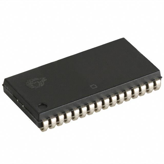
• High speed — 15 ns • Automatic power-down when deselected • Low active power — 660 mW • Low standby power — 140 mW • CMOS for optimum speed/power • TTL-compatible inputs and outputs • Easy memory expansion with CE1, CE2, and OE features provided by an active-LOW chip enable (CE1), an active-HIGH chip enable (CE2), an active-LOW output enable (OE), and three-state drivers. The device has an automatic power-down feature that reduces power consumption by more than 75% when deselected. Writing to the device is accomplished by taking CE1 and write enable (WE) inputs LOW and CE2 input HIGH. Data on the nine I/O pins (I/Oo – I/O8) is then written into the location specified on the address pins (A0 – A14). Reading from the device is accomplished by taking CE1 and OE LOW while forcing WE and CE2 HIGH. Under these conditions, the contents of the memory location specified by the address pins will appear on the I/O pins. The nine input/output pins (I/O0 – I/O8) are placed in a high-impedance state when the device is deselected (CE1 HIGH or CE2 LOW), the outputs are disabled (OE HIGH), or during a write operation (CE1 LOW, CE2 HIGH, and WE LOW). The CY7C188 is available in standard 300-mil-wide SOJs.
Functional Description
The CY7C188 is a high-performance CMOS static RAM organized as 32,768 words by 9 bits. Easy memory expansion is
Logic Block Diagram
Pin Configuration
DIP/SOJ Top View
NC NC A8 A7 A6 A5 A4 A3 A2 A1 A0 I/O0 I/O1 I/O2 I/O3 GND 1 2 3 4 5 6 7 8 9 10 11 12 13 14 15 16 32 31 30 29 28 27 26 25 24 23 22 21 20 19 18 17 VCC A14 CE2 WE A13 A9 A10 A11 OE A12 CE1 I/O8 I/O7 I/O6 I/O5 I/O4
I/O0
INPUT BUFFER
I/O1 I/O2
SENSE AMPS
A0 A1 A2 A3 A4 A5 A6
ROW DECODER
I/O3 I/O4 I/O5
32K x 9 ARRAY
C188–2
I/O6
CE1 CE2 WE OE COLUMN DECODER POWER DOWN
I/O7 I/O8
C188–1
Selection Guide
7C188–15 Maximum Access Time (ns) Maximum Operating Current (mA) Commercial Maximum Standby Current (mA) 15 120 35 7C188–20 20 170 35 7C188–25 25 165 35 7C188–35 35 160 30
Cypress Semiconductor Corporation Document #: 38-05053 Rev. **
A7 A8 A9 A 10 A 11 A 12 A 13 A 14
•
3901 North First Street
•
San Jose
•
CA 95134 • 408-943-2600 Revised August 24, 2001
�CY7C188
Maximum Ratings
(Above which the useful life may be impaired. For user guidelines, not tested.) Storage Temperature ................................. –65°C to +150°C Ambient Temperature with Power Applied............................................. –55°C to +125°C Supply Voltage on VCC Relative to GND (Pin 32 to Pin 16) .......................................... –0.5V to + 7.0V DC Voltage Applied to Outputs in High Z State[1] .................................... –0.5V to VCC + 0.5V DC Input Voltage[1] ................................. –0.5V to VCC + 0.5V Output Current into Outputs (LOW)............................. 20 mA Static Discharge Voltage .......................................... >2001V (per MIL-STD-883, Method 3015) Latch-Up Current.................................................... >200 mA
Operating Range
Range Commercial Ambient Temperature 0°C to +70°C VCC 5V ± 10%
Electrical Characteristics Over the Operating Range[2]
7C188–15 Parameter VOH VOL VIH VIL IIX IOZ IOS ICC Description Output HIGH Voltage Output LOW Voltage Input HIGH Voltage Input LOW Voltage[1] Input Load Current Output Leakage Current Output Short Circuit Current[3] VCC Operating Supply Current Automatic CE Power-Down Current— TTL Inputs Automatic CE Power-Down Current — CMOS Inputs GND ≤ VI ≤ VCC GND ≤ VI ≤ VCC, Output Disabled VCC = Max., VOUT = GND VCC = Max., IOUT = 0 mA, f = fMAX = 1/tRC Max. VCC, CE1 ≥ VIH or CE2 ≤ VIL, VIN ≥ VIH or VIN ≤ VIL, f = fMAX Max. VCC, CE1 ≥ VCC –0.3V or CE2 ≤ 0.3V, VIN ≥ VCC – 0.3V or VIN ≤ 0.3V, f = 0 Test Conditions VCC = Min., IOH = –4.0 mA VCC = Min., IOL = 8.0 mA 2.2 –0.5 –5 –5 Min. 2.4 0.4 VCC + 0.3 0.8 +5 +5 –300 120 2.2 –0.5 –5 –5 Max 7C188–20 Min. 2.4 0.4 VCC + 0.3 0.8 +5 +5 –300 170 2.2 –0.5 –5 –5 Max. 7C188–25 Min. 2.4 0.4 VCC + 0.3 0.8 +5 +5 –300 165 2.2 –0.5 –5 –5 Max. 7C188–35 Min. 2.4 0.4 VCC + 0.3 0.8 +5 +5 –300 160 Max. Unit V V V V µA µA mA mA
ISB1
35
35
35
30
mA
ISB2
10
15
15
15
mA
Capacitance[4]
Parameter CIN: Addresses CIN: Controls COUT Description Input Capacitance Input Capacitance Output Capacitance Test Conditions TA = 25°C, f = 1 MHz, VCC = 5.0V Max. 6 8 8 Unit pF pF pF
Notes: 1. Minimum voltage is equal to –2.0V for pulse durations less than 20 ns. 2. .See the last page of this specification for Group A subgroup testing information. 3. Not more than one output should be shorted at one time. Duration of the short circuit should not exceed 30 seconds. 4. Tested initially and after any design or process changes that may affect these parameters.
Document #: 38-05053 Rev. **
Page 2 of 8
�CY7C188
AC Test Loads and Waveforms[5, 6]
R1 481Ω 5V OUTPUT 30 pF INCLUDING JIGAND SCOPE Equivalent to: R2 255Ω 5V OUTPUT 5 pF INCLUDING JIGAND SCOPE R2 255Ω 3.0V 10% GND R1 481Ω ALLINPUTPULSES 90% 90% 10%
≤ 3 ns
≤ 3 ns
C188–4
(a)
167Ω
(b)
C188–3
THÉ VENIN EQUIVALENT 1.73V
OUTPUT
Switching Characteristics Over the Operating Range[2, 5]
7C188–15 Parameter READ CYCLE tRC tAA tOHA tACE tDOE tLZOE tHZOE tLZCE tHZCE tPU tPD tWC tSCE tAW tHA tSA tPWE tSD tHD tHZWE tLZWE Read Cycle Time Address to Data Valid Data Hold from Address Change CE1 LOW or CE2 HIGH to Data Valid OE LOW to Data Valid OE LOW to Low Z
[7] [6,7]
7C188–20 Min. 20 Max.
7C188–25 Min. 25 Max.
7C188–35 Min. 35 Max. Unit ns 35 3 35 16 3 15 3 15 0 20 35 22 30 0 0 22 15 0 ns ns ns ns ns ns ns ns ns ns ns ns ns ns ns ns ns ns 15 ns ns
Description
Min. 15
Max.
15 3 15 7 0 7 3 7 0 15 15 10 10 0 0 10 8 0 0 3 7 20 15 15 0 0 15 10 0 0 3 0 3
[6, 7]
20 3 20 9 0 9 3 9 0 20 25 18 20 0 0 18 10 0 7 0 3 3 3
25 25 10 11 11 20
OE HIGH to High Z
CE1 LOW or CE2 HIGH to Low Z[7] CE1 HIGH or CE2 LOW to High Z CE1 LOW or CE2 HIGH to Power-Up CE1 HIGH or CE2 LOW to Power-Down Write Cycle Time CE1 LOW or CE2 HIGH to Write End Address Set-Up to Write End Address Hold from Write End Address Set-Up to Write Start WE Pulse Width Data Set-Up to Write End Data Hold from Write End WE LOW to High Z WE HIGH to Low Z
[6] [6, 7]
WRITE CYCLE[8, 9]
11
0 3
Document #: 38-05053 Rev. **
Page 3 of 8
�CY7C188
Switching Characteristics Over the Operating Range[2, 5]
7C188–15 Parameter Description Min. Max. 7C188–20 Min. Max. 7C188–25 Min. Max. 7C188–35 Min. Max. Unit
Notes: 5. Test conditions assume signal transition time of 3 ns or less, timing reference levels of 1.5V, input pulse levels of 0 to 3.0V, and output loading of the specified IOL/IOH and 30-pF load capacitance. 6. tHZOE, tHZCE, and tHZWE are specified with CL = 5 pF as in part (b) of AC Test Loads. Transition is measured ±500 mV from steady-state voltage. 7. At any given temperature and voltage condition, tHZCE is less than tLZCE, tHZOE is less than tLZOE, and tHZWE is less than tLZWE for any given device. 8. The internal write time of the memory is defined by the overlap of CE1, LOW, CE2 HIGH, and WE LOW. All three signals must be asserted to initiate a write and any signal can terminate a write by being deasserted. The data input set-up and hold timing should be referenced to the rising edge of the signal that terminates the write. 9. The minimum write cycle time for write cycle #3 (WE controlled, OE LOW) is the sum of tHZWE and tSD.
Switching Waveforms
Read Cycle No. 1[10,11]
tRC ADDRESS tOHA DATA OUT PREVIOUS DATA VALID tAA DATA VALID
C188–5
Read Cycle No. 2 (Chip-Enable Controlled)
[11,12,13]
tRC CE1 tACE OE tDOE tLZOE HIGH IMPEDANCE tLZCE VCC SUPPLY CURRENT tPU 50% tPD ICC 50% ISB
C188–6
tHZOE tHZCE DATA VALID
HIGH IMPEDANCE
DATA OUT
Write Cycle No. 1 (WE Controlled)[8,13,14,15]
Document #: 38-05053 Rev. **
Page 4 of 8
�CY7C188
Switching Waveforms (Continued)
tWC ADDRESS
CE1 tAW tSA WE OE tSD DATA I/O NOTE 16 tHZOE
Notes: 10. Device is continuously selected. OE, CE = VIL. 11. WE is HIGH for read cycle. 12. Address valid prior to or coincident with CE transition LOW. 13. Timing parameters are the same for all chip enable signals (CE1 and CE2), so only the timing for CE1 is shown. 14. Data I/O is high impedance if OE = VIH. 15. If CE goes HIGH simultaneously with WE HIGH, the output remains in a high-impedance state. 16. During this period, the I/Os are in the output state and input signals should not be applied. [8,13,14,15]
tHA tPWE
tHD
DATA IN VALID
C188–7
Write Cycle No.2 (CE Controlled)
tWC ADDRESS tSCE CE1 tSA tAW tHA
WE tSD DATA I/O DATA IN VALID
C188–8
tHD
Write Cycle No. 3 (WE Controlled, OE LOW)[9,13,15]
Document #: 38-05053 Rev. **
Page 5 of 8
�CY7C188
Switching Waveforms (Continued)
tWC ADDRESS
CE tAW tSA WE tSD DATA I/O NOTE 16 tHZWE DATA IN VALID tLZWE
C188–9
tHA
tHD
Truth Table
CE H L L L WE X H L H OE X L X H Input/Output High Z Data Out Data In High Z Read Write Deselect, Output Disabled Mode Deselect/Power-Down Power Standby (ISB) Active (ICC) Active (ICC) Active (ICC)
Ordering Information
Speed (ns) 15 20 25 35 Ordering Code CY7C188–15VC CY7C188–20VC CY7C188–25VC CY7C188–35VC Package Name V32 V32 V32 V32 Package Type 32-Lead (300-Mil) Molded SOJ 32-Lead (300-Mil) Molded SOJ 32-Lead (300-Mil) Molded SOJ 32-Lead (300-Mil) Molded SOJ Operating Range Commercial Commercial
MILITARY SPECIFICATIONS Group A Subgroup Testing DC Characteristics
Parameter VOH VOL VIH VIL Max. Subgroups 1, 2, 3 1, 2, 3 1, 2, 3 1, 2, 3
DC Characteristics
Parameter IIX IOZ ICC ISB1 ISB2 Subgroups 1, 2, 3 1, 2, 3 1, 2, 3 1, 2, 3 1, 2, 3
Document #: 38-05053 Rev. **
Page 6 of 8
�CY7C188
Switching Characteristics
Parameter READ CYCLE tRC tAA tOHA tACE tDOE WRITE CYCLE tWC tSCE tAW tHA tSA tPWE tSD tHD 7, 8, 9, 10, 11 7, 8, 9, 10, 11 7, 8, 9, 10, 11 7, 8, 9, 10, 11 7, 8, 9, 10, 11 7, 8, 9, 10, 11 7, 8, 9, 10, 11 7, 8, 9, 10, 11 7, 8, 9, 10, 11 7, 8, 9, 10, 11 7, 8, 9, 10, 11 7, 8, 9, 10, 11 7, 8, 9, 10, 11 Subgroups
Package Diagrams
32-Lead (300-Mil) Molded SOJ V32
Document #: 38-05053 Rev. **
Page 7 of 8
© Cypress Semiconductor Corporation, 2001. The information contained herein is subject to change without notice. Cypress Semiconductor Corporation assumes no responsibility for the use of any circuitry other than circuitry embodied in a Cypress Semiconductor product. Nor does it convey or imply any license under patent or other rights. Cypress Semiconductor does not authorize its products for use as critical components in life-support systems where a malfunction or failure may reasonably be expected to result in significant injury to the user. The inclusion of Cypress Semiconductor products in life-support systems application implies that the manufacturer assumes all risk of such use and in doing so indemnifies Cypress Semiconductor against all charges.
�CY7C188
Document Title: CY7C188 32K x 9 Static RAM Document Number: 38-05053 REV. ** ECN NO. 107155 Issue Date 09/10/01 Orig. of Change SZV Description of Change Change from Spec number: 38-00220 to 38-05053
Document #: 38-05053 Rev. **
Page 8 of 8
�