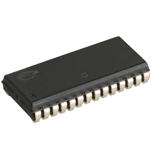
CY7C192
64 K × 4 Static RAM with Separate IO
64 K × 4 Static RAM with Separate IO
Features
Functional Description
■
High speed
❐ 15 ns
■
CMOS for optimum speed/power
■
Low active power
❐ 860 mW
The CY7C192 is a high performance CMOS static RAM
organized as 65,536 × 4 bits with separate IO. Easy memory
expansion is provided by active LOW Chip Enable (CE) and
tri-state drivers. It has an automatic power down feature that
reduces power consumption by 75% when deselected.
Writing to the device is accomplished when the Chip Enable (CE)
and Write Enable (WE) inputs are both LOW.
■
Low standby power
❐ 55 mW
■
TTL-compatible inputs and outputs
■
Automatic power down when deselected
■
Available in Pb-free 28-pin Molded SOJ package
Data on the four input pins (I0 through I3) is written into the
memory location specified on the address pins (A0 through A15).
Reading the device is accomplished by taking the Chip Enable
(CE) LOW while the Write Enable (WE) remains HIGH. Under
these conditions, the contents of the memory location specified
on the address pins appears on the four data output pins.
The output pins stay in high impedance state when Write Enable
(WE) is LOW or Chip Enable (CE) is HIGH.
A die coat ensures alpha immunity.
Logic Block Diagram
I0
I1
I2
I3
INPUT BUFFER
SENSE AMPS
O0
ROW DECODER
A0
A1
A2
A3
A4
A5
A6
A7
A8
A9
64K x 4
ARRAY
O1
O2
O3
POWER
DOWN
CE
A15
A10
A11
A12
A13
A14
COLUMN
DECODER
WE
Cypress Semiconductor Corporation
Document Number: 38-05047 Rev. *I
•
198 Champion Court
•
San Jose, CA 95134-1709
•
408-943-2600
Revised April 19, 2013
�CY7C192
Contents
Pin Configurations ........................................................... 3
Selection Guide ................................................................ 3
Maximum Ratings ............................................................. 4
Operating Range ............................................................... 4
Electrical Characteristics ................................................. 4
Capacitance ...................................................................... 4
AC Test Loads and Waveforms ....................................... 5
Switching Characteristics ................................................ 6
Switching Waveforms ...................................................... 7
Typical DC and AC Characteristics ................................ 9
Ordering Information ...................................................... 10
Ordering Code Definitions ......................................... 10
Document Number: 38-05047 Rev. *I
Package Diagram ............................................................ 11
Acronyms ........................................................................ 12
Document Conventions ................................................. 12
Units of Measure ....................................................... 12
Document History Page ................................................. 13
Sales, Solutions, and Legal Information ...................... 14
Worldwide Sales and Design Support ....................... 14
Products .................................................................... 14
PSoC Solutions ......................................................... 14
Page 2 of 14
�CY7C192
Pin Configurations
Figure 1. 28-pin Molded SOJ pinout
Top View
A6
A7
A8
A9
A10
A11
A12
A13
A14
A15
I0
I1
CE
GND
1
2
3
4
5
6
7
8
9
10
11
12
13
14
28
27
26
25
24
23
22
21
20
19
18
17
16
15
VCC
A5
A4
A3
A2
A1
A0
I3
I2
O3
O2
O1
O0
WE
Selection Guide
Description
-15
Unit
Maximum Access Time
15
ns
Maximum Operating Current
145
mA
Maximum CMOS Standby Current
10
mA
Document Number: 38-05047 Rev. *I
Page 3 of 14
�CY7C192
DC Input Voltage[1] 0.5 V to VCC + 0.5 V
Maximum Ratings
Output Current into Outputs (LOW) ............................ 20 mA
Exceeding maximum ratings may shorten the useful life of the
device. User guidelines are not tested.
Static Discharge Voltage
(per MIL-STD-883, Method 3015) ........................... > 900 V
Storage Temperature 65 °C to +150 °C
Latch-Up Current .................................................. > 200 mA
Ambient Temperature with
Power Applied 55 °C to +125 °C
Operating Range
Supply Voltage to Ground Potential 0.5 V to +7.0 V
Range
DC Voltage Applied to Outputs
in High Z State [1] 0.5 V to VCC 0.5 V
Ambient Temperature [2]
VCC
0 °C to +70 °C
5 V 10%
Commercial
Electrical Characteristics
Over the Operating Range
Parameter
Description
Test Conditions
VOH
Output HIGH Voltage
VCC = Min, IOH = 4.0 mA
VOL
Output LOW Voltage
VCC = Min, IOL = 8.0 mA
VIH
Input HIGH Voltage
[1]
-15
Unit
Min
Max
2.4
–
V
–
0.4
V
2.2
VCC + 0.3
V
0.5
0.8
V
+5
A
VIL
Input LOW Voltage
IIX
Input Leakage Current
GND < VI < VCC
5
IOZ
Output Leakage Current
GND < VO < VCC, Output Disabled
5
+5
A
ICC
VCC Operating Supply Current
VCC = Max, IOUT = 0 mA, f = fMAX = 1/tRC
–
145
mA
ISB1
Automatic CE Power Down
Current – TTL Inputs
Max VCC, CE > VIH, VIN > VIH or VIN < VIL, f = fMAX
–
30
mA
ISB2
Automatic CE Power Down
Current – CMOS Inputs
Max VCC, CE > VCC 0.3 V,
VIN > VCC 0.3 V or VIN < 0.3 V, f = 0
–
10
mA
Max
Unit
8
pF
10
pF
Capacitance
Parameter
CIN
[3]
COUT
[3]
Description
Input Capacitance
Test Conditions
TA = 25 °C, f = 1 MHz, VCC = 5.0 V
Output Capacitance
Notes
1. Minimum voltage is equal to –2.0 V for pulse durations of less than 20 ns.
2. TA is the case temperature.
3. Tested initially and after any design or process changes that may affect these parameters.
Document Number: 38-05047 Rev. *I
Page 4 of 14
�CY7C192
AC Test Loads and Waveforms
Figure 2. AC Test Loads and Waveforms
R1 481
5V
OUTPUT
R1 481
5V
OUTPUT
R2
255
30 pF
INCLUDING
JIG AND
SCOPE
(a)
Document Number: 38-05047 Rev. *I
ALL INPUT PULSES
3.0 V
R2
255
5 pF
INCLUDING
JIG AND
SCOPE
(b)
GND
10%
90%
< 3 ns
90%
10%
< 3 ns
Equivalent to:
THÉVENIN EQUIVALENT
167
OUTPUT
1.73 V
Page 5 of 14
�CY7C192
Switching Characteristics
Over the Operating Range
Parameter [4]
Description
-15
Min
Max
Unit
Read Cycle
tRC
Read Cycle Time
15
–
ns
tAA
Address to Data Valid
–
15
ns
tOHA
Output Hold from Address Change
3
–
ns
tACE
CE LOW to Data Valid
–
15
ns
[5]
tLZCE
CE LOW to Low Z
3
–
ns
tHZCE
CE HIGH to High Z [5, 6]
–
7
ns
tPU
CE LOW to Power Up
0
–
ns
CE HIGH to Power Down
–
15
ns
tWC
Write Cycle Time
15
–
ns
tSCE
CE LOW to Write End
10
–
ns
tAW
Address Setup to Write End
10
–
ns
tHA
Address Hold from Write End
0
–
ns
tSA
Address Setup to Write Start
0
–
ns
tPWE
WE Pulse Width
9
–
ns
tSD
Data Setup to Write End
9
–
ns
tHD
Data Hold from Write End
0
–
ns
tLZWE
WE HIGH to Low Z [5]
3
–
ns
–
7
ns
tPD
Write Cycle
tHZWE
[7]
WE LOW to High Z
[5, 6]
Notes
4. Test conditions assume signal transition time of 3 ns or less, timing reference levels of 1.5 V, input pulse levels of 0 to 3.0 V, and output loading of the specified IOL/IOH
and 30-pF load capacitance.
5. At any temperature and voltage condition, tHZCE is less than tLZCE, tHZW\E is less than tLZWE for any given device. These parameters are guaranteed by design and
not 100% tested.
6. tHZCE and tHZWE are specified with CL = 5 pF as in part (b) of Figure 2. Transition is measured 500 mV from steady-state voltage.
7. The internal write time of the memory is defined by the overlap of CE LOW and WE LOW. Both signals must be LOW to initiate a write and either signal can terminate
a write by going HIGH. The data input setup and hold timing must be referenced to the rising edge of the signal that terminates the write.
Document Number: 38-05047 Rev. *I
Page 6 of 14
�CY7C192
Switching Waveforms
Figure 3. Read Cycle No. 1 [8, 9]
tRC
ADDRESS
tAA
tOHA
DATA OUT
PREVIOUS DATA VALID
DATA VALID
Figure 4. Read Cycle No. 2 [8, 10]
tRC
CE
tACE
DATA OUT
tHZCE
HIGH IMPEDANCE
DATA VALID
tLZCE
VCC
SUPPLY
CURRENT
HIGH
IMPEDANCE
tPD
tPU
ICC
50%
50%
ISB
Figure 5. Write Cycle No. 1 (WE Controlled) [11]
Notes
8. WE is HIGH for read cycle.
9. Device is continuously selected, CE = VIL.
10. Address valid prior to or coincident with CE transition LOW.
11. The internal write time of the memory is defined by the overlap of CE LOW and WE LOW. Both signals must be LOW to initiate a write and either signal can
terminate a write by going HIGH. The data input setup and hold timing must be referenced to the rising edge of the signal that terminates the write.
Document Number: 38-05047 Rev. *I
Page 7 of 14
�CY7C192
Switching Waveforms (continued)
Figure 6. Write Cycle No. 2 (CE Controlled) [12, 13]
Notes
12. The internal write time of the memory is defined by the overlap of CE LOW and WE LOW. Both signals must be LOW to initiate a write and either signal can
terminate a write by going HIGH. The data input setup and hold timing must be referenced to the rising edge of the signal that terminates the write.
13. If CE goes HIGH simultaneously with WE HIGH, the output remains in a high impedance state.
Document Number: 38-05047 Rev. *I
Page 8 of 14
�CY7C192
1.4
SB
ICC
0.8
0.6
VIN =5.0V
TA =25C
0.4
0.2
1.0
0.8
0.6
VCC =5.0V
VIN =5.0V
0.4
0.2
ISB
0.0
4.0
1.2
4.5
5.0
5.5
ISB
0.0
–55
6.0
NORMALIZED ACCESS TIME
vs. AMBIENT TEMPERATURE
1.4
1.6
1.3
1.4
NORMALIZED tAA
NORMALIZED tAA
NORMALIZED ACCESS TIME
vs. SUPPLY VOLTAGE
1.2
TA =25C
1.0
1.2
1.0
VCC =5.0V
0.8
0.9
0.8
4.0
4.5
5.0
5.5
0.6
-55
6.0
TYPICAL POWER ON CURRENT
vs. SUPPLY VOLTAGE
2.5
25.0
DELTA t AA (ns)
30.0
2.0
1.5
1.0
25
2.0
3.0
4.0
SUPPLY VOLTAGE (V)
Document Number: 38-05047 Rev. *I
80
VCC =5.0V
TA =25C
60
40
20
0
0.0
5.0
2.0
3.0
4.0
OUTPUT VOLTAGE (V)
140
OUTPUT SINK CURRENT
vs. OUTPUT VOLTAGE
120
100
80
60
VCC =5.0V
TA =25C
40
20
0
0.0
125
20.0
15.0
VCC =4.5V
TA =25C
10.0
0.0
1.0
1.0
2.0
3.0
4.0
OUTPUT VOLTAGE (V)
NORMALIZED I CC vs. CYCLE TIME
1.25
5.0
0.5
1.0
100
TYPICAL ACCESS TIME CHANGE
vs. OUTPUT LOADING
3.0
0.0
0.0
120
AMBIENT TEMPERATURE (C)
SUPPLY VOLTAGE (V)
NORMALIZED IPO
125
OUTPUT SOURCE CURRENT
vs. OUTPUT VOLTAGE
AMBIENT TEMPERATURE(C)
SUPPLY VOLTAGE (V)
1.1
25
OUTPUT SINK CURRENT (mA)
1.0
NORMALIZED ICC
NORMALIZED ICC
1.2
ICC
0
200
400
600
800 1000
CAPACITANCE (pF)
NORMALIZED ICC
SB
1.4
NORMALIZED SUPPLY CURRENT
vs. AMBIENT TEMPERATURE
NORMALIZED SUPPLY CURRENT
vs. SUPPLY VOLTAGE
OUTPUT SOURCE CURRENT (mA)
Typical DC and AC Characteristics
1.00
VCC =5.0V
TA =25C
VIN =0.5V
0.75
0.50
10
20
30
40
CYCLE FREQUENCY (MHz)
Page 9 of 14
�CY7C192
Ordering Information
Speed
(ns)
15
Package
Diagram
Ordering Code
CY7C192-15VXC
Package Type
51-85031 28-pin Molded SOJ (Pb-free)
Operating
Range
Commercial
Ordering Code Definitions
CY 7 C 1 92 - 15
V
X
C
Temperature Range:
C = Commercial
Pb-free
Package Type:
V = 28-pin Molded SOJ
Speed: 15 ns
Density: 92 = 256-Kbit density with datawidth × 4 bits
Family Code: 1 = Fast Asynchronous SRAM family
Technology Code: C = CMOS
Marketing Code: 7 = SRAM
Company ID: CY = Cypress
Document Number: 38-05047 Rev. *I
Page 10 of 14
�CY7C192
Package Diagram
Figure 7. 28-pin SOJ (300 Mils) V28.3 (Molded SOJ V21) Package Outline, 51-85031
51-85031 *E
Document Number: 38-05047 Rev. *I
Page 11 of 14
�CY7C192
Acronyms
Acronym
Document Conventions
Description
Units of Measure
CE
Chip Enable
CMOS
Complementary Metal Oxide Semiconductor
°C
degree Celcius
I/O
Input/Output
MHz
megahertz
SOJ
Small Outline J-lead
µA
microampere
SRAM
Static Random Access Memory
mA
milliampere
TTL
Transistor-Transistor Logic
mm
millimeter
WE
Write Enable
ms
millisecond
mW
milliwatt
ns
nanosecond
Document Number: 38-05047 Rev. *I
Symbol
Unit of Measure
ohm
%
percent
pF
picofarad
V
volt
W
watt
Page 12 of 14
�CY7C192
Document History Page
Document Title: CY7C192, 64 K × 4 Static RAM with Separate IO
Document Number: 38-05047
Rev.
ECN No.
Issue Date
Orig. of
Change
**
107149
09/10/01
SZV
Change Spec number from: 38-00076 to 38-05047
*A
359716
See ECN
AJU
Changed Static Discharge Voltage limit in the Maximum Ratings section (page
2) from 2001V to 900V
Removed references to CY7C191
*B
419549
See ECN
AJU
Added Pb-free parts to the Ordering Information table and replaced the
Package Name column with Package Diagram
*C
492500
See ECN
NXR
Removed 20 ns and 25 ns speed bins
Changed the Low active power from 220 mW to 55 mW
Changed the description of IIX from Input Load Current to Input Leakage
Current in DC Electrical Characteristics table
Removed IOS parameter from DC Electrical Characteristics table
Removed 28-Lead (300-Mil) PDIP package from product offering
Updated Ordering Information table
*D
2104606
See ECN
*E
2956606
06/18/2010
Description of Change
VKN/AESA Removed 12 ns speed bin
KAO
Removed inactive part from Ordering Information
Updated Package Diagram.
Added Sales, Solutions, and Legal Information.
*F
3105329
12/09/2010
AJU
*G
3217855
04/06/2011
PRAS
Added Acronyms and Units of Measure.
Updated in new template.
Added Ordering Code Definitions.
*H
3271782
06/01/2011
PRAS
Updated Features.
*I
3974483
04/19/2013
MEMJ
Updated Switching Waveforms (Updated Figure 5, Figure 6).
Updated Package Diagram:
spec 51-85031 – Changed revision from *D to *E.
Completing Sunset Review.
Document Number: 38-05047 Rev. *I
Page 13 of 14
�CY7C192
Sales, Solutions, and Legal Information
Worldwide Sales and Design Support
Cypress maintains a worldwide network of offices, solution centers, manufacturer’s representatives, and distributors. To find the office
closest to you, visit us at Cypress Locations.
Products
Automotive
Clocks & Buffers
Interface
Lighting & Power Control
PSoC Solutions
cypress.com/go/automotive
cypress.com/go/clocks
psoc.cypress.com/solutions
cypress.com/go/interface
PSoC 1 | PSoC 3 | PSoC 5
cypress.com/go/powerpsoc
cypress.com/go/plc
Memory
cypress.com/go/memory
Optical & Image Sensing
cypress.com/go/image
PSoC
cypress.com/go/psoc
Touch Sensing
cypress.com/go/touch
USB Controllers
Wireless/RF
cypress.com/go/USB
cypress.com/go/wireless
© Cypress Semiconductor Corporation, 2001-2013. The information contained herein is subject to change without notice. Cypress Semiconductor Corporation assumes no responsibility for the use of
any circuitry other than circuitry embodied in a Cypress product. Nor does it convey or imply any license under patent or other rights. Cypress products are not warranted nor intended to be used for
medical, life support, life saving, critical control or safety applications, unless pursuant to an express written agreement with Cypress. Furthermore, Cypress does not authorize its products for use as
critical components in life-support systems where a malfunction or failure may reasonably be expected to result in significant injury to the user. The inclusion of Cypress products in life-support systems
application implies that the manufacturer assumes all risk of such use and in doing so indemnifies Cypress against all charges.
Any Source Code (software and/or firmware) is owned by Cypress Semiconductor Corporation (Cypress) and is protected by and subject to worldwide patent protection (United States and foreign),
United States copyright laws and international treaty provisions. Cypress hereby grants to licensee a personal, non-exclusive, non-transferable license to copy, use, modify, create derivative works of,
and compile the Cypress Source Code and derivative works for the sole purpose of creating custom software and or firmware in support of licensee product to be used only in conjunction with a Cypress
integrated circuit as specified in the applicable agreement. Any reproduction, modification, translation, compilation, or representation of this Source Code except as specified above is prohibited without
the express written permission of Cypress.
Disclaimer: CYPRESS MAKES NO WARRANTY OF ANY KIND, EXPRESS OR IMPLIED, WITH REGARD TO THIS MATERIAL, INCLUDING, BUT NOT LIMITED TO, THE IMPLIED WARRANTIES
OF MERCHANTABILITY AND FITNESS FOR A PARTICULAR PURPOSE. Cypress reserves the right to make changes without further notice to the materials described herein. Cypress does not
assume any liability arising out of the application or use of any product or circuit described herein. Cypress does not authorize its products for use as critical components in life-support systems where
a malfunction or failure may reasonably be expected to result in significant injury to the user. The inclusion of Cypress’ product in a life-support systems application implies that the manufacturer
assumes all risk of such use and in doing so indemnifies Cypress against all charges.
Use may be limited by and subject to the applicable Cypress software license agreement.
Document Number: 38-05047 Rev. *I
Revised April 19, 2013
All products and company names mentioned in this document may be the trademarks of their respective holders.
Page 14 of 14
�