CY7C194BN
256 Kb (64K x 4) Static RAM
General Description [1]
Features
• Fast access time: 15 ns and 25 ns
• Wide voltage range: 5.0V ± 10% (4.5V to 5.5V)
• CMOS for optimum speed/power
• TTL-compatible inputs and outputs
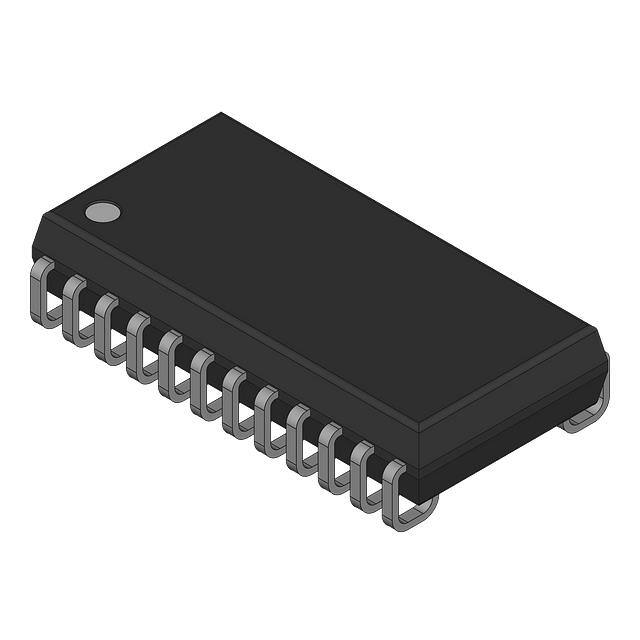
• CY7C194BN is available in 24 DIP, 24 SOJ packages.
The CY7C194BN is a high-performance CMOS
Asynchronous SRAM organized as 64K × 4 bits that supports
an asynchronous memory interface. The device features an
automatic power-down feature that significantly reduces
power consumption when deselected.
See the Truth Table in this data sheet for a complete
description of read and write modes.
The CY7C194BN is available in 24 DIP, 24 SOJ package(s).
Logic Block Diagram
Sense Amps
Row Decoder
Input Buffer
RAM Array
I/Ox
CE
WE
Power
Down
Circuit
Column Decoder
OE
(7C195 only)
X
A
X
Product Portfolio
Maximum Access Time
-15
-25
Unit
15
25
ns
Maximum Operating Current
80
80
mA
Maximum CMOS Standby Current
10
10
mA
Notes:
1. For best-practice recommendations, please refer to the Cypress application note System Design Guidelines on www.cypress.com.
Cypress Semiconductor Corporation
Document #: 001-06446 Rev. **
•
198 Champion Court
•
San Jose, CA 95134-1709
•
408-943-2600
Revised February 1, 2006
[+] Feedback
�CY7C194BN
Pin Layout and Specification
CY7C194BN 24 SOJ (8 × 15 × 3.5 mm)
A6
1
24
VCC
A7
2
23
A5
A8
3
22
A4
A9
4
21
A3
A10
5
20
A2
A11
6
19
A1
A12
7
18
A0
A13
8
17
I/O3
A14
9
16
I/O2
A15
10
15
I/O1
CE
11
14
I/O0
GND
12
13
WE
CY7C194BN 24 DIP (6.6 × 31.8 × 3.5 mm)
Document #: 001-06446 Rev. **
A6
1
24
VCC
A7
2
23
A5
A8
3
22
A4
A9
4
21
A3
A10
5
20
A2
A11
6
19
A1
A12
7
18
A0
A13
8
17
I/O3
A14
9
16
I/O2
A15
10
15
I/O1
CE
11
14
I/O0
GND
12
13
WE
Page 2 of 10
[+] Feedback
�CY7C194BN
Pin Description
CY7C194BN
Pin
Type
Description
AX
Input
Address Inputs.
CE
Control
Chip Enable.
I/OX
Input or Output
Data Input/Outputs.
24 DIP
24 SOJ
1, 2, 3, 4, 5, 6, 7, 8, 9, 10,
18, 19, 20, 21, 22, 23
1, 2, 3, 4, 5, 6, 7, 8, 9, 10,
18, 19, 20, 21, 22, 23
11
11
14, 15, 16, 17
14, 15, 16, 17
No Connect. Pins are not
internally connected to the die.
–
–
Supply
Power (5.0V).
24
24
Control
Write Enable.
13
13
NC
–
VCC
WE
CY7C194BN Truth Table
CE
WE
I/Ox
Mode
Power
H
X
High Z
Power-Down
Standby (ISB)
L
H
Data Out
Read
Active (ICC)
L
L
Data In
Write
Active (ICC)
Document #: 001-06446 Rev. **
Page 3 of 10
[+] Feedback
�CY7C194BN
Maximum Ratings (Above which the useful life may be impaired. For user guidelines, not tested.)
Parameter
Description
Value
Unit
TSTG
Storage Temperature
–65 to +150
°C
TAMB
Ambient Temperature with Power Applied (i.e. case temperature)
–55 to +125
°C
VCC
Core Supply Voltage Relative to VSS
VIN, VOUT
DC Voltage Applied to any Pin Relative to VSS
–0.5 to +7.0
V
–0.5 to VCC + 0.5
V
IOUT
Output Short-Circuit Current
20
mA
VESD
Static Discharge Voltage (per MIL-STD-883, Method 3015)
> 2001
V
ILU
Latch-up Current
> 200
mA
Operating Range
Range
Ambient Temperature (TA)
Voltage Range (VCC)
Commercial
0°C to 70°C
5.0V ± 10%
DC Electrical Characteristics[3]
15 ns
Parameter
Description
Condition
25 ns
Min.
Max.
Min.
Max.
Unit
VIH
Input HIGH Voltage
2.2
VCC + 0.3
2.2
VCC + 0.3
V
VIL
Input LOW Voltage
–0.3
0.8
–0.5
0.8
V
VOH
Output HIGH Voltage VCC = Min., loh = –4.0 ma
2.4
–
2.4
–
V
VOL
Output LOW Voltage
–
0.4
–
0.4
V
ICC
VCC Operating Supply VCC = Max., IOUT = 0 mA,
Current
f = FMAX = 1 / tRC
–
80
–
80
mA
ISB1
Automatic CE
Power-down Current
TTL Inputs
VCC = Max., CE ≥ VIH, VIN ≥
VIH or VIN ≤ VIL, f = FMAX
–
30
–
30
mA
ISB2
Automatic CE
Power-down Current
CMOS Inputs
VCC = Max., CE ≥ VCC - 0.3v,
VIN > VCC - 0.3v or VIN ≤ 0.3,
f = 0, Commercial
–
10
–
10
mA
IOZ
Output Leakage
Current
GND ≤ Vi ≤ VCC,
Output Disabled
–5
+5
–5
+5
µA
IIX
Input Load Current
GND ≤ Vi ≤ VCC
–5
+5
–5
+5
µA
VCC = Min., lol = 8.0 ma
Capacitance[2]
Parameter
Description
CIN
Input Capacitance
COUT
Output Capacitance
Conditions
Max
Unit
TA = 25°C, f = 1 MHz, VCC = 5.0V
7
pF
10
Thermal Resistance[4]
CY7C194BN
Parameter
Description
ΘJA
Thermal Resistance
(Junction to Ambient)
ΘJC
Thermal Resistance
(Junction to Case)
Conditions
24 DIP
24 SOJ
Unit
Still Air, soldered on a 3 x 4.5
square inches, two-layer
printed circuit board
75.69
84.15
°C/W
33.80
37.56
Note:
2. Tested initially and after any design or process change that may affect these parameters
3. VIL(min) = –2.0V for pulse durations of less than 20 ns.
4. Test Conditions assume a transition time of 3ns or less, timing reference levels of 1.5V, input pulse levels of 0 to 3.0V
Document #: 001-06446 Rev. **
Page 4 of 10
[+] Feedback
�CY7C194BN
AC Test Loads
Output Loads
Output Loads
for tHZOE
for , tHZCE & tHZWE
R1
R3
VCC
VCC
Output
C1
R2
C2
(A)*
(B)*
All Input Pulses
Thevenin Equivalent
Output
Rth
R4
VCC
90%
90%
VT
VSS
10%
10%
Rise Time
1 V/ns
Fall Time
1 V/ns
* including scope and jig capacitance
AC Test Conditions
Parameter
C1
Description
Capacitor 1
Nom.
Unit
30
pF
C2
Capacitor 2
5
R1
Resistor 1
480
R2
Resistor 2
255
R3
Resistor 3
480
R4
Resistor 4
255
RTH
Resistor Thevenin
167
VTH
Voltage Thevenin
1.73
Document #: 001-06446 Rev. **
Ω
V
Page 5 of 10
[+] Feedback
�CY7C194BN
AC Electrical Characteristics[2, 5, 6, 7]
15 ns
Parameter
Description
25 ns
Min
Max
Min
Max
Unit
tRC
Read Cycle Time
15
–
25
–
ns
tAA
Address to Data Valid
–
15
–
25
ns
tOHA
Data Hold from Address Change
3
–
3
–
ns
tACE
CE to Data Valid
–
15
–
25
ns
tLZCE
CE to Low Z
3
–
3
–
ns
tHZCE
CE to High Z
–
7
–
10
ns
tPU
CE to Power-up
0
–
0
–
ns
tPD
CE to Power-down
–
15
–
25
ns
tWC
Write Cycle Time
15
–
25
–
ns
tSCE
CE to Write End
10
–
18
–
ns
tAW
Address Set-up to Write End
10
–
20
–
ns
tHA
Address Hold from Write End
0
–
0
–
ns
tSA
Address Set-up to Write Start
0
–
0
–
ns
tPWE
WE Pulse Width
9
–
18
–
ns
tSD
Data Set-Up to Write End
8
–
10
–
ns
tHD
Data Hold from Write End
0
–
0
–
ns
tHZWE
WE LOW to High Z
–
7
-
10
ns
tLZWE
WE HIGH to Low Z
3
–
3
–
ns
Timing Waveforms
Read Cycle No. 1[8, 9]
tRC
Address
tAA
tOHA
Data Out
Previous Data Valid
Data Valid
Notes:
5. At any given temperature and voltage condition, tHZCE is less than tLZCE, and tHZWE is less than tLZWE for any given device.
6. The internal write time of the memory is defined by the overlap of CE LOW and WE LOW. CE and WE must be LOW to initiate a write, and the transition of any
of these signals can terminate the write. The input data set-up and hold timing should be referenced to the leading edge of the signal that terminates the write.
7. tHZCE, tHZWE are specified as in part (b) of the A/C Test Loads. Transitions are measured ± 200 mV from steady state voltage.
8. Device is continuously selected. CE = VIL.
9. WE is HIGH for Read Cycle.
Document #: 001-06446 Rev. **
Page 6 of 10
[+] Feedback
�CY7C194BN
Timing Waveforms (continued)
Read Cycle No. 2[2, 10, 11]
tRC
Address
CE
tHZCE
t ACE
OE
tDOE
tHZOE
tLZOE
High Z
High Z
Data Out
Data Valid
tLZCE
tPU
ICC
V CC
tPD
50%
ISB
Current
50%
Write Cycle No. 1 (WE Controlled)[2, 12]
t WC
Address
tSCE
CE
tAW
tHA
tPWE
tSA
WE
tSD
Data
In/Out
Undefined
tHD
Undefined
See Footnotes
Data-In Valid
see footnotes
tHZWE
tLZWE
Notes:
10. WE is HIGH in read cycle.
11. Address valid prior to or coincident with CE transition LOW.
12. The minimum write cycle time is the sum of tHZWE and tSD.
Document #: 001-06446 Rev. **
Page 7 of 10
[+] Feedback
�CY7C194BN
Timing Waveforms (continued)
Write Cycle No. 2 (CE Controlled)[13, 14]
tWC
Address
tSCE
CE
tSA
tHA
tAW
WE
tSD
Data In/Out
High Z
Data-In Valid
tHD
High Z
Notes:
13. This cycle is CE controlled.
14. If CE goes HIGH simultaneously with WE going HIGH, the output remains in a high-impedance state.
Document #: 001-06446 Rev. **
Page 8 of 10
[+] Feedback
�CY7C194BN
Ordering Information
Speed
(ns)
Ordering Code
15
25
Package
Diagram
Package Type
Power Option
Operating
Range
CY7C194BN-15PC
51-85013
24 DIP (6.6 x 31.8 x 3.5 mm)
Standard
Commercial
CY7C194BN-15VC
51-85030
24 SOJ (8 x 15 x 3.5 mm)
Standard
Commercial
CY7C194BN-25VC
51-85030
24 SOJ (8 x 15 x 3.5 mm)
Standard
Commercial
Please contact local sales representative regarding availability of these parts.
Package Diagrams
24-lead (300-mil) SOJ (51-85030)
PIN 1 ID
12
1
MIN.
DIMENSIONS IN INCHES[MM]
MAX.
REFERENCE JEDEC MO-088
0.291[7.39]
0.300[7.62]
0.330[8.38]
0.350[8.89]
PACKAGE WEIGHT 0.75gms
PART #
13
24
0.597[15.16]
0.613[15.57]
V24.3
STANDARD PKG.
VZ24.3
LEAD FREE PKG.
SEATING PLANE
0.120[3.05]
0.140[3.55]
0.007[0.17]
0.013[0.33]
0.004[0.10]
0.050[1.27]
TYP.
0.025[0.63] MIN.
0.262[6.65]
0.272[6.91]
0.013[0.33]
0.019[0.48]
51-85030-*B
24 DIP (6.6 x 31.8 x 3.5 mm) (51-85013)
51-85013-*B
All product and company names mentioned in this document may be the trademarks of their respective holders.
Document #: 001-06446 Rev. **
Page 9 of 10
© Cypress Semiconductor Corporation, 2006. The information contained herein is subject to change without notice. Cypress Semiconductor Corporation assumes no responsibility for the use
of any circuitry other than circuitry embodied in a Cypress product. Nor does it convey or imply any license under patent or other rights. Cypress products are not warranted nor intended to be
used for medical, life support, life saving, critical control or safety applications, unless pursuant to an express written agreement with Cypress. Furthermore, Cypress does not authorize its
products for use as critical components in life-support systems where a malfunction or failure may reasonably be expected to result in significant injury to the user. The inclusion of Cypress
products in life-support systems application implies that the manufacturer assumes all risk of such use and in doing so indemnifies Cypress against all charges.
[+] Feedback
�CY7C194BN
Document History Page
Document Title: CY7C194BN 256 Kb (64K x 4) Static RAM
Document Number: 001-06446
REV.
ECN No.
Issue Date
Orig. of
Change
**
424111
See ECN
NXR
Document #: 001-06446 Rev. **
Description of Change
New Data Sheet
Page 10 of 10
[+] Feedback
�