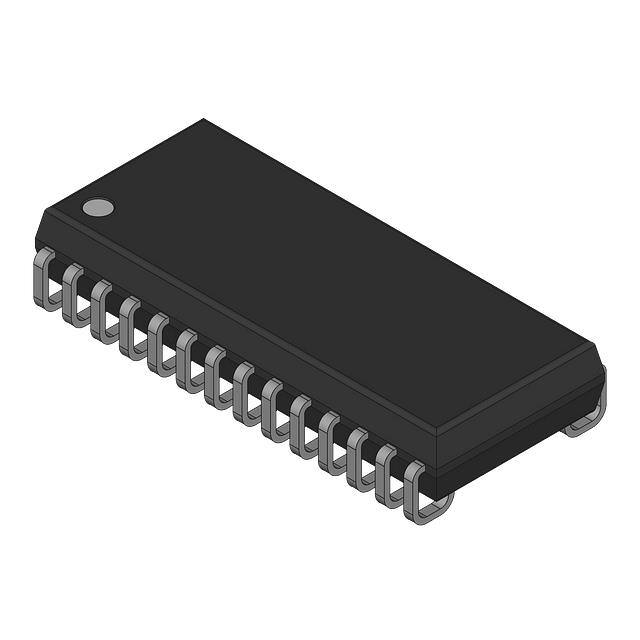
CY7C199CN
256 K (32 K × 8) Static RAM
Features
General Description [1]
■
Fast access time: 15 ns
■
Wide voltage range: 5.0 V ± 10% (4.5 V to 5.5 V)
■
complementary metal oxide semiconductor (CMOS) for
optimum speed and power
The CY7C199CN is a high performance CMOS Asynchronous
SRAM organized as 32K by 8 bits that supports an asynchronous
memory interface. The device features an automatic
power-down feature that reduces power consumption when
deselected.
■
Transistor transistor logic (TTL) compatible inputs and outputs
See the “Truth Table” on page 4 in this data sheet for a complete
description of read and write modes.
■
2.0 V data retention
■
Low CMOS standby power
The CY7C199CN is available in 28-pin molded SOJ and 28-pin
DIP package(s).
■
Automated power-down when deselected
■
Available in Pb-free 28-pin molded small outline J-lead (SOJ)
and 28-pin DIP packages
Logic Block Diagram
RAM Array
Sense Amps
Row Decoder
Input Buffer
I/Ox
CE
Column Decoder
WE
Power
Down
Circuit
OE
X
A
X
Product Portfolio
–15
Unit
15
ns
Maximum operating current
80
mA
Maximum CMOS standby current (low power)
500
μA
Maximum access time
Cypress Semiconductor Corporation
Document #: 001-06435 Rev. *G
•
198 Champion Court
•
San Jose, CA 95134-1709
•
408-943-2600
Revised August 2, 2011
�CY7C199CN
Contents
Pin Layout and Specifications ........................................ 3
Pin Description ................................................................. 4
Truth Table ........................................................................ 4
Maximum Ratings ............................................................. 4
Operating Range ............................................................... 4
Capacitance ...................................................................... 5
Thermal Resistance .......................................................... 5
DC Electrical Characteristics .......................................... 5
AC Test Loads .................................................................. 6
AC Test Conditions .......................................................... 6
AC Electrical Characteristics .......................................... 7
Data Retention Characteristics ....................................... 7
Document #: 001-06435 Rev. *G
Ordering Information ...................................................... 12
Ordering Code Definitions ......................................... 12
Package Diagrams .......................................................... 13
Acronyms ........................................................................ 15
Document Conventions ................................................. 15
Units of Measure ....................................................... 15
Document History Page ................................................. 16
Sales, Solutions, and Legal Information ...................... 17
Worldwide Sales and Design Support ....................... 17
Products .................................................................... 17
PSoC Solutions ......................................................... 17
Page 2 of 17
�CY7C199CN
Pin Layout and Specifications
28 DIP
A5
A6
A7
1
2
3
28 SOJ
28
27
26
VCC
A5
1
28
VCC
WE
A6
2
27
WE
A7
3
26
A4
A8
4
25
A3
A4
A8
4
25
A3
A9
5
24
A2
A9
5
24
A2
A10
6
23
A1
A10
6
23
A1
A11
7
22
OE
A11
7
22
OE
A12
8
21
A0
A12
8
21
A0
A13
9
20
CE
A13
9
20
CE
A14
10
19
IO7
A14
10
19
IO7
IO0
11
18
IO6
IO0
11
18
IO6
IO5
IO1
12
17
IO5
IO2
13
16
IO4
VSS
14
15
IO3
IO1
IO2
VSS
12
13
14
17
16
15
IO4
IO3
Note
1. For best practices recommendations, refer to the Cypress application note System Design Guidelines on www.cypress.com.
Document #: 001-06435 Rev. *G
Page 3 of 17
�CY7C199CN
Pin Description
Pin
Type
Description
DIP
SOJ
1, 2, 3, 4, 5, 6, 7, 8, 9,
10, 21, 23, 24, 25, 26
1, 2, 3, 4, 5, 6, 7, 8, 9, 10,
21, 23, 24, 25, 26
20
20
11, 12, 13, 15, 16, 17,
18, 19
11, 12, 13, 15, 16, 17, 18,
19
AX
Input
Address inputs
CE
Control
Chip enable
IOX
Input or Output
Data input outputs
OE
Control
Output enable
22
22
VCC
Supply
Power (5.0V)
28
28
VSS
Supply
Ground
14
14
WE
Control
Write enable
27
27
Truth Table
CE
OE
WE
IOx
Mode
Power
H
X
X
High-Z
Deselect/Power-down
Stand by (ISB)
L
L
H
Data Out
Read
Active (ICC)
L
X
L
Data In
Write
Active (ICC)
L
H
H
High-Z
Selected, Outputs disabled
Active (ICC)
Maximum Ratings
Exceeding maximum ratings may shorten the useful life of the device. User guidelines are not tested.
Parameter
Description
Value
Unit
TSTG
Storage temperature
–65 to +150
°C
TAMB
Ambient temperature with power applied (that is, case temperature)
–55 to +125
°C
VCC
Core Supply voltage relative to VSS
–0.5 to +7.0
V
VIN, VOUT
DC voltage applied to any pin relative to VSS
–0.5 to VCC + 0.5
IOUT
Output short-circuit current
20
VESD
Static discharge voltage (in accordance with MIL-STD-883, Method 3015)
> 2001
V
ILU
Latch-up current
> 200
mA
V
mA
Operating Range
Range
Ambient Temperature (TA)
Voltage Range (VCC)
Commercial
0 °C to 70 °C
5.0 V ± 10%
–40 °C to 85 °C
5.0 V ± 10%
Industrial
Document #: 001-06435 Rev. *G
Page 4 of 17
�CY7C199CN
DC Electrical Characteristics
Over the Operating Range [2]
–15
Parameter
Description
Condition
Unit
Min
Max
VIH
Input HIGH voltage
2.2
VCC + 0.3
V
VIL
Input LOW voltage
–0.5
0.8
V
VOH
Output HIGH voltage
VCC = Min, IOH = –4.0 mA
2.4
–
V
VOL
Output LOW voltage
VCC = Min, IOL = 8.0 mA
–
0.4
V
ICC
VCC Operating supply
current
VCC = Max, IOUT = 0 mA,
f = Fmax = 1/tRC
–
80
mA
ISB1
Automatic CE power-down Max VCC, CE ≥ VIH,
current TTL inputs
VIN ≥ VIH or VIN ≤ VIL, f = Fmax
–
30
mA
–
10
mA
–
10
mA
–
500
μA
L
Automatic CE power-down Max VCC, CE ≥ VCC – 0.3 V,
current CMOS Inputs
VIN ≥ VCC – 0.3 V, or VIN ≤ 0.3 V, f = 0
ISB2
L
IOZ
Output leakage current
GND ≤ VI ≤ VCC, output disabled
–5
+5
μA
IIX
Input leakage current
GND ≤ VI ≤ VCC
–5
+5
μA
Capacitance
Parameter[3]
Description
CIN
Input capacitance
COUT
Output capacitance
Conditions
Max
Unit
TA = 25°C, f = 1 MHz, VCC = 5.0 V
8
pF
8
Thermal Resistance
Parameter[3]
Description
θJA
Thermal resistance
(junction to ambient)
θJC
Thermal resistance
(junction to case)
Conditions
SOJ
DIP
Unit
Still air, soldered on a 3 × 4.5 square
inch, two–layer printed circuit board
79
69.33
°C/W
41.42
31.62
Note
2. VIL (min) = –2.0 V for pulse durations of less than 20 ns.
Document #: 001-06435 Rev. *G
Page 5 of 17
�CY7C199CN
AC Test Loads
O u tp u t L o a d s
O u tp u t L o a d s
fo r t H Z O E , t H Z C E & t H Z W E
R1
R3
VC C
VC C
O u tp u t
C1
R2
C2
(A )*
(B )*
A ll In p u t P u ls e s
T h e v e n in E q u iv a le n t
O u tp u t
R th
R4
VC C
90%
90%
VT
10%
VS S
10%
R is e T im e
1 V /n s
F a ll T im e
1 V /n s
* in c lu d in g s c o p e a n d jig c a p a c ita n c e
AC Test Conditions
Parameter
Description
Nom
Unit
pF
C1
Capacitor 1
30
C2
Capacitor 2
5
R1
Resistor 1
480
R2
Resistor 2
255
R3
Resistor 3
480
R4
Resistor 4
255
RTH
Resistor Thevenin
167
VTH
Voltage Thevenin
1.73
Ω
V
Note
3. Tested initially and after any design or process change that may affect these parameters.
Document #: 001-06435 Rev. *G
Page 6 of 17
�CY7C199CN
AC Electrical Characteristics
–15
Parameter[4]
Description
Unit
Min
Max
tRC
Read cycle time
15
–
ns
tAA
Address to data valid
–
15
ns
tOHA
Data hold from address change
3
–
ns
tACE
CE to data valid
–
15
ns
tDOE
OE to data valid
–
7
ns
0
–
ns
[5]
tLZOE
OE to Low-Z
tHZOE
OE to High-Z [5, 6]
–
7
ns
CE to Low-Z
[5]
3
–
ns
tHZCE
CE to High-Z
[5, 6]
–
7
ns
tPU
CE to Power-up
0
–
ns
tPD
CE to Power-down
–
15
ns
15
–
ns
tLZCE
[7]
tWC
Write Cycle Time
tSCE
CE to write end
10
–
ns
tAW
Address setup to write end
10
–
ns
tHA
Address hold from write end
0
–
ns
tSA
Address setup to write start
0
–
ns
tPWE
WE pulse width
9
–
ns
tSD
Data setup to write end
9
–
ns
tHD
Data hold from write end
tHZWE
tLZWE
0
–
ns
WE LOW to High-Z
[5, 6]
–
7
ns
WE HIGH to Low-Z
[5]
3
–
ns
Data Retention Characteristics
Parameter[8]
Description
VDR
VCC for data retention
ICCDR
Data retention current
tCDR
Chip deselect to data
retention time
tR
Operation recovery time
Condition
VCC = VDR = 2.0 V, CE ≥ VCC – 0.3 V,
VIN ≥ VCC – 0.3 V or VIN ≤ 0.3 V
Min
Max
Unit
2.0
–
V
–
150
μA
0
–
ns
200
–
μs
Notes
4. Test Conditions are based on a transition time of 3 ns or less and timing reference levels of 1.5 V, and input pulse levels of 0 to 3.0 V.
5. At any given temperature and voltage condition, tHZCE is less than tLZCE, tHZOE is less than tLZOE, and tHZWE is less than tLZWE for any given device.
6. tHZOE, tHZCE, tHZWE are specified as in part (b) of the “” on page 5. Transitions are measured ± 200 mV from steady state voltage.
7. The internal memory write time is defined by the overlap of CE LOW and WE LOW. CE and WE must be LOW to initiate a write, and the transition of any of these
signals can terminate the write. The input data setup and hold timing must be referenced to the leading edge of the signal that terminates the write.
8. L-version only.
Document #: 001-06435 Rev. *G
Page 7 of 17
�CY7C199CN
Timing Waveforms
Data Retention Waveform
VCC
DATA RETENTION MODE
tCDR
tR
CE
Figure 1. Read Cycle 1 [9, 10]
tRC
Address
tAA
tOHA
Data Out
Previous Data Valid
Data Valid
Notes
9. Device is continuously selected. OE = VIL = CE.
10. WE is HIGH for read cycle.
Document #: 001-06435 Rev. *G
Page 8 of 17
�CY7C199CN
Timing Waveforms
(continued)
Figure 2. Read Cycle 2 [11, 12]
tRC
Address
CE
tHZCE
tACE
OE
tDOE
tHZOE
tLZOE
High Z
High Z
Data Out
VCC
Current
Data Valid
ICC
ISB
tLZCE
tPU
tPD
50%
50%
Notes
11. This cycle is OE controlled and WE is HIGH read cycle.
12. Address valid before or similar with CE transition LOW.
Document #: 001-06435 Rev. *G
Page 9 of 17
�CY7C199CN
Timing Waveforms
(continued)
Figure 3. Write Cycle 1 (WE controlled) [13, 14, 15]
tWC
Address
tSCE
CE
tAW
tHA
tPWE
tSA
WE
OE
tHD
tHZOE
Data In/Out
tSD
Undefined
Data-In Valid
see footnotes
Figure 4. Write Cycle 2 (CE controlled) [14, 16, 17]
tWC
Address
tSCE
CE
tSA
tHA
tAW
WE
tSD
Data In/Out
High Z
Data-In Valid
tHD
High Z
Notes
13. This cycle is WE controlled, OE is HIGH during write.
14. Data in and/or out is high impedance if OE = VIH.
15. During this period the IOs are in output state and input signals must not be applied.
16. This cycle is CE controlled.
17. If CE goes HIGH simultaneously with WE going HIGH, the output remains in a high impedance state.
Document #: 001-06435 Rev. *G
Page 10 of 17
�CY7C199CN
Timing Waveforms
(continued)
Figure 5. Write Cycle 3 (WE controlled, OE low) [18]
t WC
Address
tSCE
CE
tAW
tHA
t PWE
tSA
WE
tSD
Data
In Out
Undefined
tHD
Undefined
See Footnotes
Data In Valid
see footnotes
t HZWE
t LZWE
Note
18. The cycle is WE controlled, OE LOW. The minimum write cycle time is the sum of tHZWE and tSD.
Document #: 001-06435 Rev. *G
Page 11 of 17
�CY7C199CN
Ordering Information
Contact local sales representative regarding availability of these parts.
Speed
(ns)
15
Ordering Code
Package
Diagram
Package Type
Power Option
Operating
Range
CY7C199CN-15PXC
51-85014
28 DIP (6.9 × 35.6 × 3.5 mm), Pb-free
Standard
Commercial
CY7C199CNL-15VXI
51-85031
28-Pin (300-Mil) Molded SOJ, Pb-free
Low Power
Industrial
Ordering Code Definitions
CY 7 C 1 99 CN L - XX XX X
Temperature Range: X = C or I
C = Commercial; I = Industrial
Package Type: XX = VX or PX or ZX
VX = 28-lead Molded SOJ (Pb-free)
PX = 28-lead DIP (Pb-free)
Speed: XX = 15 ns
L = low power
CN = 0.25 µm Technology
99 = 256 K bit density with datawidth × 8 bits
1 = Fast Asynchronous SRAM family
Technology Code: C = CMOS
7 = SRAM
CY = Cypress
Document #: 001-06435 Rev. *G
Page 12 of 17
�CY7C199CN
Package Diagrams
Figure 6. 28-pin (300 Mil) Molded SOJ, 51-85031
51-85031 *E
Document #: 001-06435 Rev. *G
Page 13 of 17
�CY7C199CN
Package Diagrams (continued)
Figure 7. 28-pin (300 Mil) PDIP, 51-85014
51-85014 *F
Document #: 001-06435 Rev. *G
Page 14 of 17
�CY7C199CN
Acronyms
Document Conventions
Acronym
Description
CE
chip enable
CMOS
complementary metal oxide semiconductor
I/O
input/output
OE
output enable
SRAM
static random access memory
SOJ
small outline j-lead
VFBGA
very fine-pitch ball grid array
Document #: 001-06435 Rev. *G
Units of Measure
Symbol
Unit of Measure
ns
nanosecond
V
volt
µA
microampere
mA
milliampere
mV
millivolt
mW
milliwatt
MHz
megahertz
pF
picoFarad
°C
degree Celsius
W
Watt
Page 15 of 17
�CY7C199CN
Document History Page
Document Title: CY7C199CN, 256 K (32 K × 8) Static RAM
Document Number: 001-06435
Revision
ECN
Submission
Date
Orig. of
Change
Description of Change
**
430363
See ECN
NXR
New Data Sheet
*A
684342
See ECN
VKN
Added Automotive-A Information
Updated Ordering Information Table
*B
839904
See ECN
VKN
Added tDOE spec for Automotive-A part in AC Electrical characteristics
table
*C
2896044
03/19/2010
NXR
Updated Ordering Information Table
Updated Package Diagram
*D
3108898
12/13/2010
PRAS
Added Ordering Code Definitions.
*E
3198636
03/17/11
PRAS
Dislodged Automotive device information to 001-67737
Updated template and styles.
*F
3246329
05/04/2011
PRAS
Additional information on ISB1, ISB2 with respect to L parts
*G
3302830
08/02/2011
RAME
Removed the following parts from ordering information table.
CY7C199CN-15VXC
CY7C199CN-20ZXI
Removed all information related to 28-pin TSOP 1.
Removed all information related to 20 ns speed bin.
Removed spec 51-85071.
Document #: 001-06435 Rev. *G
Page 16 of 17
�CY7C199CN
Sales, Solutions, and Legal Information
Worldwide Sales and Design Support
Cypress maintains a worldwide network of offices, solution centers, manufacturer’s representatives, and distributors. To find the office
closest to you, visit us at Cypress Locations.
Products
Automotive
Clocks & Buffers
Interface
Lighting & Power Control
PSoC Solutions
cypress.com/go/automotive
cypress.com/go/clocks
psoc.cypress.com/solutions
cypress.com/go/interface
PSoC 1 | PSoC 3 | PSoC 5
cypress.com/go/powerpsoc
cypress.com/go/plc
Memory
Optical & Image Sensing
PSoC
Touch Sensing
USB Controllers
Wireless/RF
cypress.com/go/memory
cypress.com/go/image
cypress.com/go/psoc
cypress.com/go/touch
cypress.com/go/USB
cypress.com/go/wireless
© Cypress Semiconductor Corporation, 2006-2011. The information contained herein is subject to change without notice. Cypress Semiconductor Corporation assumes no responsibility for the use of
any circuitry other than circuitry embodied in a Cypress product. Nor does it convey or imply any license under patent or other rights. Cypress products are not warranted nor intended to be used for
medical, life support, life saving, critical control or safety applications, unless pursuant to an express written agreement with Cypress. Furthermore, Cypress does not authorize its products for use as
critical components in life-support systems where a malfunction or failure may reasonably be expected to result in significant injury to the user. The inclusion of Cypress products in life-support systems
application implies that the manufacturer assumes all risk of such use and in doing so indemnifies Cypress against all charges.
Any Source Code (software and/or firmware) is owned by Cypress Semiconductor Corporation (Cypress) and is protected by and subject to worldwide patent protection (United States and foreign),
United States copyright laws and international treaty provisions. Cypress hereby grants to licensee a personal, non-exclusive, non-transferable license to copy, use, modify, create derivative works of,
and compile the Cypress Source Code and derivative works for the sole purpose of creating custom software and or firmware in support of licensee product to be used only in conjunction with a Cypress
integrated circuit as specified in the applicable agreement. Any reproduction, modification, translation, compilation, or representation of this Source Code except as specified above is prohibited without
the express written permission of Cypress.
Disclaimer: CYPRESS MAKES NO WARRANTY OF ANY KIND, EXPRESS OR IMPLIED, WITH REGARD TO THIS MATERIAL, INCLUDING, BUT NOT LIMITED TO, THE IMPLIED WARRANTIES
OF MERCHANTABILITY AND FITNESS FOR A PARTICULAR PURPOSE. Cypress reserves the right to make changes without further notice to the materials described herein. Cypress does not
assume any liability arising out of the application or use of any product or circuit described herein. Cypress does not authorize its products for use as critical components in life-support systems where
a malfunction or failure may reasonably be expected to result in significant injury to the user. The inclusion of Cypress’ product in a life-support systems application implies that the manufacturer
assumes all risk of such use and in doing so indemnifies Cypress against all charges.
Use may be limited by and subject to the applicable Cypress software license agreement.
Document #: 001-06435 Rev. *G
Revised August 2, 2011
All products and company names mentioned in this document may be the trademarks of their respective holders.
Page 17 of 17
�