CY7C4201V/4211VCY7C4241V/4251VLow Voltage 256/512 × 9
Synchronous FIFOs
CY7C4201V/4211V
Low Voltage 256/512 × 9
Synchronous FIFOs
Low Voltage 256/512 × 9 Synchronous FIFOs
Features
Functional Description
■
High-speed, low-power, first-in, first-out (FIFO) memories
❐ 256 × 9 (CY7C4201V)
❐ 512 × 9 (CY7C4211V)
The CY7C42X1V are high-speed, low-power, FIFO memories
with clocked read and write interfaces. All are nine bits wide.
Programmable features include Almost Full/Almost Empty flags.
These FIFOs provide solutions for a wide variety of data
buffering needs, including high-speed data acquisition,
multiprocessor interfaces, and communications buffering.
■
High-speed 66-MHz operation (15-ns read/write cycle time)
■
Low power (ICC = 20 mA)
■
3.3 V operation for low power consumption and easy integration
into low-voltage systems
■
5V-tolerant inputs VIH(max) = 5 V
■
Fully asynchronous and simultaneous read and write operation
■
Empty, full, and programmable almost empty and almost full
status flags
■
TTL compatible
■
Output Enable (OE) pin
■
Independent read and write enable pins
■
Center power and ground pins for reduced noise
■
Width expansion capability
■
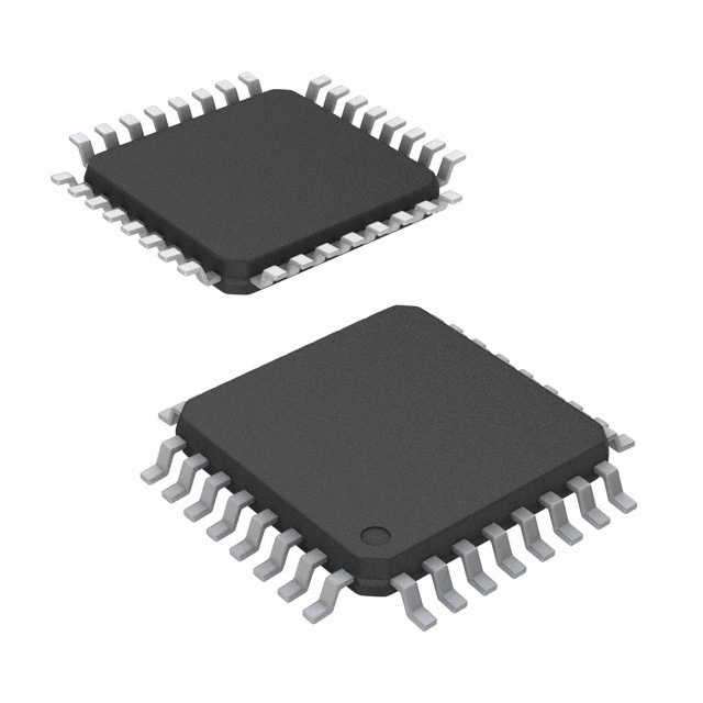
Space saving 32-pin 7 mm × 7 mm TQFP
Depth expansion is possible using one enable input for system
control, while the other enable is controlled by expansion logic to
direct the flow of data.
■
32-pin PLCC available in Pb-free Packages
For a complete list of related documentation, click here.
These FIFOs have 9-bit input and output ports that are controlled
by separate clock and enable signals. The input port is controlled
by a Free-Running Clock (WCLK) and two Write Enable pins
(WEN1, WEN2/LD).
When WEN1 is LOW and WEN2/LD is HIGH, data is written into
the FIFO on the rising edge of the WCLK signal. While WEN1,
WEN2/LD is held active, data is continually written into the FIFO
on each WCLK cycle. The output port is controlled in a similar
manner by a Free-Running Read Clock (RCLK) and two Read
Enable Pins (REN1, REN2). In addition, the CY7C42X1V has an
Output Enable Pin (OE). The Read (RCLK) and Write (WCLK)
clocks may be tied together for single clock operation or the two
clocks may be run independently for asynchronous read/write
applications. Clock frequencies up to 66 MHz are achievable.
Logic Block Diagram
Cypress Semiconductor Corporation
Document Number: 38-06010 Rev. *I
•
198 Champion Court
•
San Jose, CA 95134-1709
•
408-943-2600
Revised November 18, 2015
�CY7C4201V/4211V
Contents
Pin Configuration ............................................................. 3
Pin Definitions .................................................................. 3
Selection Guide ................................................................ 4
Architecture ...................................................................... 4
Functional Overview ........................................................ 4
Resetting the FIFO ...................................................... 4
FIFO Operation ........................................................... 4
Programming ............................................................... 5
Width Expansion Configuration ................................... 7
Flag Operation ............................................................. 7
Maximum Ratings ............................................................. 8
Operating Range ............................................................... 8
Electrical Characteristics ................................................. 8
Capacitance ...................................................................... 9
AC Test Loads and Waveforms ....................................... 9
Document Number: 38-06010 Rev. *I
Switching Characteristics .............................................. 10
Switching Waveforms .................................................... 11
Ordering Information ...................................................... 19
Ordering Code Definitions ......................................... 19
Package Diagrams .......................................................... 20
Acronyms ........................................................................ 21
Document Conventions ................................................. 21
Units of Measure ....................................................... 21
Document History Page ................................................. 22
Sales, Solutions, and Legal Information ...................... 23
Worldwide Sales and Design Support ....................... 23
Products .................................................................... 23
PSoC® Solutions ...................................................... 23
Cypress Developer Community ................................. 23
Technical Support ..................................................... 23
Page 2 of 23
�CY7C4201V/4211V
Pin Configuration
Figure 1. 32-pin TQFP pinout
Pin Definitions
Signal Name
I/O
Description
D08
Data Inputs
I
Data Inputs for 9-bit bus.
Q08
Data Outputs
O
Data Outputs for 9-bit bus.
WEN1
Write Enable 1
I
The only write enable when device is configured to have programmable flags. Data is
written on a LOW-to-HIGH transition of WCLK when WEN1 is asserted and FF is HIGH. If the FIFO
is configured to have two write enables, data is written on a LOW-to-HIGH transition of WCLK when
WEN1 is LOW and WEN2/LD and FF are HIGH.
WEN2/LD
Write Enable 2
Dual Mode Pin
Load
I
If HIGH at reset, this pin operates as a second write enable. If LOW at reset, this pin
operates as a control to write or read the programmable flag offsets. WEN1 must be LOW and
WEN2 must be HIGH to write data into the FIFO. Data will not be written into the FIFO if the FF is LOW.
If the FIFO is configured to have programmable flags, WEN2/LD is held LOW to write or read the
programmable flag offsets.
I
REN1, REN2 Read Enable
Inputs
I
Enables the device for Read operation.
WCLK
Write Clock
I
The rising edge clocks data into the FIFO when WEN1 is LOW and WEN2/LD is HIGH and
the FIFO is not Full. When LD is asserted, WCLK writes data into the programmable flag-offset register.
RCLK
Read Clock
I
The rising edge clocks data out of the FIFO when REN1 and REN2 are LOW and the FIFO
is not Empty. When WEN2/LD is LOW, RCLK reads data out of the programmable flag offset register.
EF
Empty Flag
O
When EF is LOW, the FIFO is empty. EF is synchronized to RCLK.
FF
Full Flag
O
When FF is LOW, the FIFO is full. FF is synchronized to WCLK.
PAE
Programmable
Almost Empty
O
When PAE is LOW, the FIFO is almost empty based on the almost empty offset value
programmed into the FIFO.
PAF
Programmable
Almost Full
O
When PAF is LOW, the FIFO is almost full based on the almost full offset value programmed into
the FIFO.
RS
Reset
I
Resets device to empty condition. A reset is required before an initial read or write operation
after power-up.
OE
Output Enable
I
When OE is LOW, the FIFO’s data outputs drive the bus to which they are connected. If OE is
HIGH, the FIFO’s outputs are in High Z (high-impedance) state.
Document Number: 38-06010 Rev. *I
Page 3 of 23
�CY7C4201V/4211V
Selection Guide
Description
CY7C42X1V-15
Unit
66.7
MHz
Maximum Access Time
11
ns
Minimum Cycle Time
15
ns
Minimum Data or Enable Set-up
4
ns
Minimum Data or Enable Hold
1
ns
Maximum Flag Delay
10
ns
20
mA
Maximum Frequency
Active Power Supply Current
Architecture
The CY7C42X1V consists of an array of 64 to 8K words of nine
bits each (implemented by a dual-port array of SRAM cells),
a read pointer, a write pointer, control signals (RCLK, WCLK,
REN1, REN2, WEN1, WEN2, RS), and flags (EF, PAE, PAF, FF.)
Functional Overview
The CY7C42X1V provides four status pins: Empty, Full, Almost Empty,
Almost Full. The Almost Empty/Almost Full flags are programmable to
single word granularity. The programmable flags default to Empty-7 and
Full-7.
The flags are synchronous, that is, they change state relative to
either the Read Clock (RCLK) or the Write Clock (WCLK). When
entering or exiting the Empty and Almost Empty states, the flags
are updated exclusively by the RCLK. The flags denoting Almost
Full and Full states are updated exclusively by WCLK. The
synchronous flag architecture guarantees that the flags maintain
their status for at least one cycle
All configurations are fabricated using an advanced 0.65 P-Well
CMOS technology. Input ESD protection is greater than 2001 V, and
latch-up is prevented by the use of guard rings.
Resetting the FIFO
Upon power-up, the FIFO must be reset with a Reset (RS) cycle.
This causes the FIFO to enter the Empty condition signified by
EF being LOW. All data outputs (Q0-8) go LOW tRSF after the
rising edge of RS. In order for the FIFO to reset to its default
state, a falling edge must occur on RS and the user must not read
or write while RS is LOW. All flags are guaranteed to be valid tRSF
after RS is taken LOW.
FIFO Operation
Commercial
rising edge of the WCLK signal. Similarly, when the REN1 and
REN2 signals are active LOW, data in the FIFO memory will be
presented on the Q0-8 outputs. New data will be presented on
each rising edge of RCLK while REN1 and REN2 are active.
REN1 and REN2 must set up tENS before RCLK for it to be a valid
read function. WEN1 and WEN2 must occur tENS before WCLK
for it to be a valid write function.
An Output Enable (OE) pin is provided to three-state the Q0-8
outputs when OE is asserted. When OE is enabled (LOW), data in
the output register will be available to the Q0-8 outputs after tOE.
The FIFO contains overflow circuitry to disallow additional writes
when the FIFO is full, and underflow circuitry to disallow
additional reads when the FIFO is empty. An empty FIFO
maintains the data of the last valid read on its Q0-8 outputs even
after additional reads occur.
Write Enable 1 (WEN1). If the FIFO is configured for programmable flags, Write Enable 1 (WEN1) is the only write enable
control pin. In this configuration, when Write Enable 1 (WEN1) is
LOW, data can be loaded into the input register and RAM array
on the LOW-to-HIGH transition of every write clock (WCLK).
Data is stored is the RAM array sequentially and independently
of any on-going read operation.
Write Enable 2/Load (WEN2/LD). This is a dual-purpose pin.
The FIFO is configured at Reset to have programmable flags or
to have two write enables, which allows for depth expansion. If
Write Enable 2/Load (WEN2/LD) is set active HIGH at Reset
(RS=LOW), this pin operates as a second write enable pin.
If the FIFO is configured to have two write enables, when Write
Enable (WEN1) is LOW and Write Enable 2/Load (WEN2/LD) is
HIGH, data can be loaded into the input register and RAM array
on the LOW-to-HIGH transition of every write clock (WCLK.)
Data is stored in the RAM array sequentially and independently
of any on-going read operation.
When the WEN1 signal is active LOW and WEN2 is active HIGH,
data present on the D0-8 pins is written into the FIFO on each
Document Number: 38-06010 Rev. *I
Page 4 of 23
�CY7C4201V/4211V
Programming
WEN2/LD and WEN1 are LOW writes data to the empty LSB
register again. Figure 2 shows the register sizes and default
values for the various device types.
When WEN2/LD is held LOW during Reset, this pin is the load
(LD) enable for flag offset programming. In this configuration,
WEN2/LD can be used to access the four 8-bit offset registers
contained in the CY7C42X1V for writing or reading data to these
registers.
It is not necessary to write to all the offset registers at one time.
A subset of the offset registers can be written; then by bringing
the WEN2/LD input HIGH, the FIFO is returned to normal read
and write operation. The next time WEN2/LD is brought LOW, a
write operation stores data in the next offset register in
sequence.
When the device is configured for programmable flags and both
WEN2/LD and WEN1 are LOW, the first LOW-to-HIGH transition
of WCLK writes data from the data inputs to the empty offset
Least Significant Bit (LSB) register. The second, third, and fourth
LOW-to-HIGH transitions of WCLK store data in the empty offset
Most Significant Bit (MSB) register, full offset LSB register, and
full offset MSB register, respectively, when WEN2/LD and WEN1
are LOW. The fifth LOW-to-HIGH transition of WCLK while
The contents of the offset registers can be read to the data
outputs when WEN2/LD is LOW and both REN1 and REN2 are
LOW. LOW-to-HIGH transitions of RCLK read register contents
to the data outputs. Writes and reads should not be performed
simultaneously on the offset registers.
Figure 2. Offset Register Location and Default Values
256 x 9
8
7
512 x 9
0
8
Empty Offset (LSB) Reg.
Default Value = 007h
Empty Offset (LSB) Reg.
Default Value = 007h
0
8
0
7
0
8
(MSB)
0
8
7
0
8
Full Offset (LSB) Reg
Default Value = 007h
8
7
0
Full Offset (LSB) Reg
Default Value = 007h
0
8
0
(MSB)
0
Document Number: 38-06010 Rev. *I
Page 5 of 23
�CY7C4201V/4211V
Programmable Flag (PAE, PAF) Operation
Whether the flag offset registers are programmed as described
in Table 1 or the default values are used, the programmable
Almost Empty Flag (PAE) and programmable Almost Full Flag
(PAF) states are determined by their corresponding offset
registers and the difference between the read and write pointers.
Table 1. Writing the Offset Registers
WCLK[1]
LD
WEN
0
0
Empty Offset (LSB)
Empty Offset (MSB)
Full Offset (LSB)
Full Offset (MSB)
Selection
0
1
No Operation
1
0
Write Into FIFO
1
1
No Operation
to the LOW-to-HIGH transition of RCLK by one flip-flop and is
LOW when the FIFO contains n or fewer unread words. PAE is
set HIGH by the LOW-to-HIGH transition of RCLK when the
FIFO contains (n+1) or greater unread words.
The number formed by the full offset least significant bit register
and full offset most significant bit register is referred to as m and
determines the operation of PAF. PAF is synchronized to the
LOW-to-HIGH transition of WCLK by one flip-flop and is set LOW
when the number of unread words in the FIFO is greater than or
equal to CY7C4201V (256 – m) and CY7C4211V (512 – m). PAF
is set HIGH by the LOW-to-HIGH transition of WCLK when the
number of available memory locations is greater than m.
The number formed by the empty offset least significant bit
register and empty offset most significant register is referred to
as n and determines the operation of PAE. PAE is synchronized
Table 2. Status Flags
Number of Words in FIFO
CY7C4201V
CY7C4211V
0
0
1 to n[2]
1 to n[2]
(n+1) to 128
(n+1) to 256
129 to (256(m+1))
257 to (512(m+1))
(512m)[3] to 511
(256m)[3] to 255
256
512
FF
PAF
PAE
EF
H
H
H
H
H
L
H
H
H
H
L
L
L
L
H
H
H
H
L
H
H
H
H
H
Notes
1. The same selection sequence applies to reading from the registers. REN1 and REN2 are enabled and a read is performed on the LOW-to-HIGH transition of RCLK.
2. n = Empty Offset (n=7 default value).
3. m = Full Offset (m=7 default value).
Document Number: 38-06010 Rev. *I
Page 6 of 23
�CY7C4201V/4211V
Width Expansion Configuration
Word width may be increased simply by connecting the corresponding input control signals of multiple devices. A composite
flag should be created for each of the end-point status flags (EF
and FF). The partial status flags (PAE and PAF) can be detected
from any one device. Figure 3 demonstrates a 18-bit word width
by using two CY7C42X1Vs. Any word width can be attained by
adding additional CY7C42X1Vs.
When the CY7C42X1V is in a width expansion configuration, the
Read Enable (REN2) control input can be grounded (see
Figure 3). In this configuration, the Write Enable 2/Load
(WEN2/LD) pin is set to LOW at Reset so that the pin operates
as a control to load and read the programmable flag offsets.
Figure 3. Block Diagram of 256 x 9, 512 x 9 Low-Voltage Synchronous FIFO Memory Used in a Width-Expansion Configuration
RESET (RS)
DATA IN (D) 18
RESET (RS)
9
9
READ CLOCK (RCLK)
WRITE CLOCK (WCLK)
READ ENABLE 1 (REN1)
WRITE ENABLE 1 (WEN1)
OUTPUT ENABLE (OE)
WRITE ENABLE 2/LOAD
(WEN2/LD)
CY7C42X1V
PROGRAMMABLE (PAF)
FULL FLAG (FF) # 1
CY7C42X1V
PROGRAMMABLE (PAE)
EMPTY FLAG (EF) #1
EF EMPTY FLAG (EF) #2
EF
FF
FF
9
FULL FLAG (FF) # 2
DATA OUT (Q)
18
9
Read Enable 2 (REN2)
Flag Operation
The CY7C42X1 devices provide four flag pins to indicate the
condition of the FIFO contents. Empty, Full, PAE, and PAF are
synchronous.
Full Flag
The Full Flag (FF) will go LOW when device is full. Write operations are inhibited whenever FF is LOW regardless of the state
Document Number: 38-06010 Rev. *I
Read Enable 2 (REN2)
of WEN1 and WEN2/LD. FF is synchronized to WCLK, i.e., it is
exclusively updated by each rising edge of WCLK.
Empty Flag
The Empty Flag (EF) will go LOW when the device is empty.
Read operations are inhibited whenever EF is LOW, regardless
of the state of REN1 and REN2. EF is synchronized to RCLK,
i.e., it is exclusively updated by each rising edge of RCLK.
Page 7 of 23
�CY7C4201V/4211V
Maximum Ratings
Output Current into Outputs (LOW) ............................ 20 mA
Static Discharge Voltage
(per MIL-STD-883, Method 3015) .......................... > 2001 V
Exceeding maximum ratings may shorten the useful life of the
device. User guidelines are not tested.
Latch up Current .................................................... > 200 mA
Storage Temperature ................................. –65 °C to +150 °C
Operating Range
Ambient Temperature with
Power Applied .......................................... –-55 °C to +125 °C
Range
Supply Voltage to Ground Potential .............–0.5 V to +5.0 V
Commercial
DC Voltage Applied to Outputs
in High-Z State .............................................–0.5 V to +5.0 V
Industrial
Ambient Temperature
VCC
0 °C to +70 °C
3.3 V 300 mV
–40 °C to +85 °C
3.3 V 300 mV
DC Input Voltage .........................................–0.5 V to +5.0 V
Electrical Characteristics
Over the Operating Range
Parameter
Description
Test Conditions
VOH
Output HIGH Voltage
VCC = Min., IOH = 2.0 mA
VOL
Output LOW Voltage
VCC = Min., IOL = 8.0 mA
VIH
7C42X1V-15
Min
Max
Unit
2.4
–
V
–
0.4
V
Input HIGH Voltage
2.0
5.0
V
VIL
Input LOW Voltage
0.5
0.8
V
IIX
Input Leakage Current
VCC = Max.
10
+10
A
IOZL
IOZH
Output OFF, High Z Current
OE > VIH,
VSS < VO < VCC
10
+10
A
ICC[4]
Active Power Supply Current
Commercial
–
20
mA
ISB[5]
Average Standby Current
Commercial
–
6
mA
Notes
4. Outputs open. Tested at Frequency = 20 MHz.
5. All inputs = VCC – 0.2 V, except WCLK and RCLK, which are switching at 20 MHz.
Document Number: 38-06010 Rev. *I
Page 8 of 23
�CY7C4201V/4211V
Capacitance
Parameter [6]
Description
CIN
Input capacitance
COUT
Output capacitance
Test Conditions
TA = 25 °C, f = 1 MHz, VCC = 5.0 V
Max
Unit
5
pF
7
pF
AC Test Loads and Waveforms
Figure 4. AC Test Loads and Waveforms [7, 8]
R1 = 330
ALL INPUT PULSES
3.3 V
OUTPUT
3.0 V
CL
R2 = 510
INCLUDING
JIG AND
SCOPE
Equivalent to:
THÉVENIN EQUIVALENT
Rth = 200
OUTPUT
GND
3 ns
90%
10%
90%
10%
3 ns
Vth = 2.0 V
Notes
6. Tested initially and after any design or process changes that may affect these parameters.
7. CL = 30 pF for all AC parameters except for tOHZ.
8. CL = 5 pF for tOHZ.
Document Number: 38-06010 Rev. *I
Page 9 of 23
�CY7C4201V/4211V
Switching Characteristics
Over the Operating Range
Parameter
Description
7C42X1V-15
Min
Max
Unit
tS
Clock Cycle Frequency
–
66.7
MHz
tA
Data Access Time
2
11
ns
tCLK
Clock Cycle Time
15
–
ns
tCLKH
Clock HIGH Time
6
–
ns
tCLKL
Clock LOW Time
6
–
ns
tDS
Data Set-Up Time
4
–
ns
tDH
Data Hold Time
1
–
ns
tENS
Enable Set-Up Time
4
–
ns
tENH
Enable Hold Time
1
–
ns
tRS
Reset Pulse Width[9]
15
–
ns
tRSS
Reset Set-Up Time
10
–
ns
tRSR
Reset Recovery Time
10
–
ns
tRSF
Reset to Flag and Output Time
–
18
ns
tOLZ
Output Enable to Output in Low Z[10]
0
–
ns
tOE
Output Enable to Output Valid
3
8
ns
3
8
ns
Z[10]
tOHZ
Output Enable to Output in High
tWFF
Write Clock to Full Flag
–
11
ns
tREF
Read Clock to Empty Flag
–
11
ns
tPAF
Clock to Programmable Almost-Full Flag
–
16
ns
tPAE
Clock to Programmable Almost-Full Flag
–
16
ns
tSKEW1
Skew Time between Read Clock and Write Clock for Empty Flag and Full Flag
6
–
ns
tSKEW2
Skew Time between Read Clock and Write Clock for Almost-Empty Flag and
Almost-Full Flag
15
–
ns
Notes
9. Pulse widths less than minimum values are not allowed.
10. Values guaranteed by design, not currently tested.
Document Number: 38-06010 Rev. *I
Page 10 of 23
�CY7C4201V/4211V
Switching Waveforms
Figure 5. Write Cycle Timing
tCLKH
tCLK
tCLKL
WCLK
tDS
tDH
D0 –D8
tENS
tENH
WEN1
NO OPERATION
NO OPERATION
WEN2
(if applicable)
tWFF
tWFF
FF
tSKEW1
[11]
RCLK
REN1,REN2
Note
11. tSKEW1 is the minimum time between a rising RCLK edge and a rising WCLK edge to guarantee that FF will go HIGH during the current clock cycle. If the time
between the rising edge of RCLK and the rising edge of WCLK is less than tSKEW1, then FF may not change state until the next WCLK rising edge.
Document Number: 38-06010 Rev. *I
Page 11 of 23
�CY7C4201V/4211V
Switching Waveforms (continued)
Figure 6. Read Cycle Timing
tCKL
tCLKH
tCLKL
RCLK
tENS
tENH
REN1,REN2
NO OPERATION
tREF
tREF
EF
tA
Q0 –Q8
VALID DATA
tOLZ
tOHZ
tOE
OE
tSKEW1
[12]
WCLK
WEN1
WEN2
Note
12. tSKEW1 is the minimum time between a rising WCLK edge and a rising RCLK edge to guarantee that EF will go HIGH during the current clock cycle. It the time
between the rising edge of WCLK and the rising edge of RCLK is less than tSKEW1, then EF may not change state until the next RCLK rising edge.
Document Number: 38-06010 Rev. *I
Page 12 of 23
�CY7C4201V/4211V
Switching Waveforms (continued)
Figure 7. Reset Timing [13]
RS
tRS
tRSS
tRSR
tRSS
tRSR
tRSS
tRSR
REN1,
REN2
WEN1
WEN2/LD
[14]
tRSF
EF,PAE
tRSF
FF,PAF,
tRSF
Q0 Q8
OE=1 [15]
OE=0
Notes
13. The clocks (RCLK, WCLK) can be free-running during reset.
14. Holding WEN2/LD HIGH during reset will make the pin act as a second enable pin. Holding WEN2/LD LOW during reset will make the pin act as a load enable
for the programmable flag offset registers.
15. After reset, the outputs will be LOW if OE = 0 and three-state if OE=1.
Document Number: 38-06010 Rev. *I
Page 13 of 23
�CY7C4201V/4211V
Switching Waveforms (continued)
Figure 8. First Data Word Latency after Reset with Simultaneous Read and Write
WCLK
tDS
D0 –D8
D0 (FIRSTVALID WRITE)
D1
D2
D3
[17]
tA
D4
tENS
tFRL
WEN1
[16]
WEN2
(if applicable)
tSKEW1
RCLK
tREF
EF
tA
REN1,
REN2
Q0 –Q8
D0
tOLZ
D1
tOE
OE
Notes
16. When tSKEW1 > minimum specification, tFRL (maximum) = tCLK + tSKEW1. When tSKEW1 < minimum specification, tFRL (maximum) = either 2*tCLK + tSKEW1 or
tCLK + tSKEW1. The Latency Timing applies only at the Empty Boundary (EF = LOW).
17. The first word is available the cycle after EF goes HIGH, always.
Document Number: 38-06010 Rev. *I
Page 14 of 23
�CY7C4201V/4211V
Switching Waveforms (continued)
Figure 9. Empty Flag Timing
WCLK
tDS
tDS
DATAWRITE2
DATAWRITE1
D0 –D8
tENH
WEN1
tENH
tENS
tENS
tENS
tENH
tENS
tENH
WEN2
(if applicable)
tFRL
[18]
tFRL
[16]
RCLK
tSKEW1
tREF
tREF
tREF
tSKEW1
EF
REN1,
REN2
LOW
OE
tA
Q0 –Q8
DATA IN OUTPUT REGISTER
DATA READ
Note
18. When tSKEW1 > minimum specification, tFRL (maximum) = tCLK + tSKEW1. When tSKEW1 < minimum specification, tFRL (maximum) = either 2*tCLK + tSKEW1 or
tCLK + tSKEW1. The Latency Timing applies only at the Empty Boundary (EF = LOW).
Document Number: 38-06010 Rev. *I
Page 15 of 23
�CY7C4201V/4211V
Switching Waveforms (continued)
Figure 10. Full Flag Timing
NO WRITE
NO WRITE
NO WRITE
WCLK
tSKEW1 [19]
tDS
tSKEW1 [19]
DATA WRITE
DATA WRITE
D0 –D8
tWFF
tWFF
tWFF
FF
WEN1
WEN2
(if applicable)
RCLK
tENS
REN1,
REN2
OE
tENH
tENS
LOW
tA
Q0 –Q8
tENH
DATA IN OUTPUT REGISTER
tA
DATA READ
NEXT DATA READ
Note
19. tSKEW1 is the minimum time between a rising RCLK edge and a rising WCLK edge to guarantee that FF will go HIGH during the current clock cycle. If the time
between the rising edge of RCLK and the rising edge of WCLK is less than tSKEW1, then FF may not change state until the next WCLK rising edge.
Document Number: 38-06010 Rev. *I
Page 16 of 23
�CY7C4201V/4211V
Switching Waveforms (continued)
Figure 11. Programmable Almost Empty Flag Timing
tCLKL
tCLKH
WCLK
tENS tENH
WEN1
WEN2
(if applicable)
tENS tENH
Note 20
PAE
N + 1 WORDS
INFIFO
tSKEW2
[21]
Note 22
tPAE
tPAE
RCLK
tENS
tENS tENH
REN1,
REN2
Figure 12. Programmable Almost Full Flag Timing
tCLKL
tCLKH
Note 23
WCLK
tENS tENH
WEN1
[24]
WEN2
(if applicable)
tENS tENH
PAF
tPAF
FULL M WORDS
IN FIFO [25]
FULL (M+1) WORDS
IN FIFO
tSKEW2 [26]
tPAF
RCLK
tENS
tENS tENH
REN1,
REN2
Notes
20. PAE offset = n.
21. tSKEW2 is the minimum time between a rising WCLK and a rising RCLK edge for PAE to change state during that clock cycle. If the time between the edge of
WCLK and the rising RCLK is less than tSKEW2, then PAE may not change state until the next RCLK.
22. If a read is performed on this rising edge of the read clock, there will be Empty + (n1) words in the FIFO when PAE goes LOW.
23. If a write is performed on this rising edge of the write clock, there will be Full– (m–1) words of the FIFO when PAF goes LOW.
24. PAF offset = m.
25. 256-m words in FIFO for CY7C4201V, 512–m words for CY7C4211V
26. tSKEW2 is the minimum time between a rising RCLK edge and a rising WCLK edge for PAF to change during that clock cycle. If the time between the rising edge
of RCLK and the rising edge of WCLK is less than tSKEW2, then PAF may not change state until the next WCLK.
Document Number: 38-06010 Rev. *I
Page 17 of 23
�CY7C4201V/4211V
Switching Waveforms (continued)
Figure 13. Write Programmable Registers
tCLK
tCLKL
tCLKH
WCLK
tENS
tENH
WEN2/LD
tENS
WEN1
tDS
tDH
D0 –D8
PAE OFFSET
LSB
PAE OFFSET
MSB
PAF OFFSET
LSB
PAF OFFSET
MSB
Figure 14. Read Programmable Registers
tCLK
tCLKL
tCLKH
RCLK
tENS
tENH
WEN2/LD
tENS
PAF OFFSET
MSB
REN1,
REN2
tA
Q0 –Q8
Document Number: 38-06010 Rev. *I
UNKNOWN
PAE OFFSET LSB
PAE OFFSET MSB
PAF OFFSET
LSB
Page 18 of 23
�CY7C4201V/4211V
Ordering Information
Speed
(ns)
Package
Name
Ordering Code
Package Type
Operating
Range
256 × 9 Low Voltage Synchronous FIFO
15
CY7C4201V-15AXC
A32
32-pin TQFP (Pb-free)
Commercial
A32
32-pin TQFP (Pb-free)
Industrial
512 × 9 Low Voltage Synchronous FIFO
15
CY7C4211V-15AXI
Ordering Code Definitions
CY
7
C
4
2X
1
V
- 15
A
X
X
Temperature Grade: X = C or I
C = Commercial; I = Industrial
Pb-free
Package Type:
A = 32-pin TQFP
Speed Grade: 15 ns
Voltage range: 3.3 V
Width: 1 = × 9
Depth: 2X = 20 or 21
20 = 256 Bytes; 21 = 512 Bytes
Family Code: 4 = FIFO
Technology Code: C = CMOS
Marketing Code: 7 = SRAM
Company ID: CY = Cypress
Document Number: 38-06010 Rev. *I
Page 19 of 23
�CY7C4201V/4211V
Package Diagrams
Figure 15. 32-pin TQFP (7 × 7 × 1.0 mm) Package Outline, 51-85063
51-85063 *E
Document Number: 38-06010 Rev. *I
Page 20 of 23
�CY7C4201V/4211V
Acronyms
Acronym
Document Conventions
Description
Units of Measure
CMOS
Complementary Metal Oxide Semiconductor
EF
Empty Flag
°C
degree Celsius
ESD
Electrostatic Discharge
k
kilohm
FF
Full Flag
MHz
megahertz
FIFO
First-In First-Out
µA
microampere
I/O
Input/Output
mA
milliampere
LSB
Least Significant Bit
mm
millimeter
MSB
Most Significant Bit
mV
millivolt
OE
Output Enable
ns
nanosecond
PAE
Programmable Almost Empty
PAF
Programmable Almost Full
RCLK
Read Clock
RS
Reset
TQFP
Thin Quad Flat Pack
TTL
Transistor-Transistor Logic
WCLK
Write Clock
Document Number: 38-06010 Rev. *I
Symbol
Unit of Measure
ohm
%
percent
pF
picofarad
V
volt
W
watt
Page 21 of 23
�CY7C4201V/4211V
Document History Page
Document Title: CY7C4201V/4211V, Low Voltage 256/512 × 9 Synchronous FIFOs
Document Number: 38-06010
Rev.
ECN
Orig. of
Change
Submission
Date
**
106471
SZV
09/10/01
Change from Spec number: 38-00622 to 38-06010
*A
127857
FSG
08/25/03
Updated Switching Waveforms:
Updated Figure 9.
Fixed typos in all figures in the section.
*B
384573
ESH
See ECN
Added Pb-free logo to top of front page.
Added industrial Temperature Range related information in all instances across
the document.
Updated Ordering Information:
Added MPNs CY7C4251V-25AXC, CY7C4251V-15AXC,
CY7C4241V-15AXC, CY7C4241V-15JXC, CY7C4241V-25XC,
CY7C4231V-25AXC, CY7C4221V-15AI, CY7C4211V-15AXI,
CY7C4201V-15AXC.
*C
2896039
RAME
03/19/2010
Removed CY7C4421V and CY7C4231V parts related information in all
instances across the document.
Updated Ordering Information:
Removed inactive parts.
Updated Package Diagrams.
*D
2965557
RAME
06/30/2010
Removed CY7C4421V, CY7C4221V, CY7C4231V, CY7C4241V and
CY7C4251V part related information in all instances across the document.
Removed 25 ns and 35 ns speed bins related information in all instances across
the document.
Updated Ordering Information:
Removed inactive parts.
*E
3094385
ADMU
11/24/10
Corrections to the PAE and PAF flags had been done in all instances across
the document.
Added Ordering Code Definitions.
*F
3847934
ADMU
12/20/2012
Updated Ordering Information (Updated part numbers).
Updated Package Diagrams:
spec 51-85063 – Changed revision from *C to *D.
*G
4215930
SMCH
12/10/2013
Added Acronyms and Units of Measure.
Updated to new template.
Completing Sunset Review.
*H
4581652
SMCH
11/26/2014
Updated Functional Description:
Added “For a complete list of related documentation, click here.” at the end.
*I
5018894
NILE
11/18/2015
Updated Package Diagrams:
spec 51-85063 – Changed revision from *D to *E.
Updated to new template.
Completing Sunset Review.
Document Number: 38-06010 Rev. *I
Description of Change
Page 22 of 23
�CY7C4201V/4211V
Sales, Solutions, and Legal Information
Worldwide Sales and Design Support
Cypress maintains a worldwide network of offices, solution centers, manufacturer’s representatives, and distributors. To find the office
closest to you, visit us at Cypress Locations.
PSoC® Solutions
Products
Automotive
cypress.com/go/automotive
Clocks & Buffers
Interface
Lighting & Power Control
Memory
cypress.com/go/clocks
cypress.com/go/interface
cypress.com/go/powerpsoc
cypress.com/go/memory
PSoC
cypress.com/go/psoc
Touch Sensing
cypress.com/go/touch
USB Controllers
Wireless/RF
psoc.cypress.com/solutions
PSoC 1 | PSoC 3 | PSoC 4 | PSoC 5LP
Cypress Developer Community
Community | Forums | Blogs | Video | Training
Technical Support
cypress.com/go/support
cypress.com/go/USB
cypress.com/go/wireless
© Cypress Semiconductor Corporation, 2001-2015. The information contained herein is subject to change without notice. Cypress Semiconductor Corporation assumes no responsibility for the use of
any circuitry other than circuitry embodied in a Cypress product. Nor does it convey or imply any license under patent or other rights. Cypress products are not warranted nor intended to be used for
medical, life support, life saving, critical control or safety applications, unless pursuant to an express written agreement with Cypress. Furthermore, Cypress does not authorize its products for use as
critical components in life-support systems where a malfunction or failure may reasonably be expected to result in significant injury to the user. The inclusion of Cypress products in life-support systems
application implies that the manufacturer assumes all risk of such use and in doing so indemnifies Cypress against all charges.
Any Source Code (software and/or firmware) is owned by Cypress Semiconductor Corporation (Cypress) and is protected by and subject to worldwide patent protection (United States and foreign),
United States copyright laws and international treaty provisions. Cypress hereby grants to licensee a personal, non-exclusive, non-transferable license to copy, use, modify, create derivative works of,
and compile the Cypress Source Code and derivative works for the sole purpose of creating custom software and or firmware in support of licensee product to be used only in conjunction with a Cypress
integrated circuit as specified in the applicable agreement. Any reproduction, modification, translation, compilation, or representation of this Source Code except as specified above is prohibited without
the express written permission of Cypress.
Disclaimer: CYPRESS MAKES NO WARRANTY OF ANY KIND, EXPRESS OR IMPLIED, WITH REGARD TO THIS MATERIAL, INCLUDING, BUT NOT LIMITED TO, THE IMPLIED WARRANTIES
OF MERCHANTABILITY AND FITNESS FOR A PARTICULAR PURPOSE. Cypress reserves the right to make changes without further notice to the materials described herein. Cypress does not
assume any liability arising out of the application or use of any product or circuit described herein. Cypress does not authorize its products for use as critical components in life-support systems where
a malfunction or failure may reasonably be expected to result in significant injury to the user. The inclusion of Cypress’ product in a life-support systems application implies that the manufacturer
assumes all risk of such use and in doing so indemnifies Cypress against all charges.
Use may be limited by and subject to the applicable Cypress software license agreement.
Document Number: 38-06010 Rev. *I
Revised November 18, 2015
All products and company names mentioned in this document may be the trademarks of their respective holders.
Page 23 of 23
�