Please note that Cypress is an Infineon Technologies Company.
The document following this cover page is marked as “Cypress” document as this is the
company that originally developed the product. Please note that Infineon will continue
to offer the product to new and existing customers as part of the Infineon product
portfolio.
Continuity of document content
The fact that Infineon offers the following product as part of the Infineon product
portfolio does not lead to any changes to this document. Future revisions will occur
when appropriate, and any changes will be set out on the document history page.
Continuity of ordering part numbers
Infineon continues to support existing part numbers. Please continue to use the
ordering part numbers listed in the datasheet for ordering.
www.infineon.com
�CY7C4255V
CY7C4275V
CY7C4285V
8K/32K/64K × 18 Low Voltage
Deep Sync FIFOs
8K/32K/64K × 18 Low Voltage Deep Sync FIFOs
Features
Functional Description
■
3.3 V operation for low power consumption and easy integration
into low voltage systems
■
High speed, low power, first-in first-out (FIFO) memories
■
8K × 18 (CY7C4255V)
■
32K × 18 (CY7C4275V)
■
64K × 18 (CY7C4285V)
■
0.35 micron CMOS for optimum speed and power
■
High speed 100 MHz operation (10 ns read/write cycle times)
■
Low power
❐ ICC = 30 mA
❐ ISB = 4 mA
■
Fully asynchronous and simultaneous read and write operation
■
Empty, Full, Half Full, and programmable Almost Empty and
Almost Full status flags
■
Retransmit function
■
Output Enable (OE) pin
■
Independent read and write enable pins
■
Supports free running 50% duty cycle clock inputs
■
Width Expansion Capability
■
Depth Expansion Capability
■
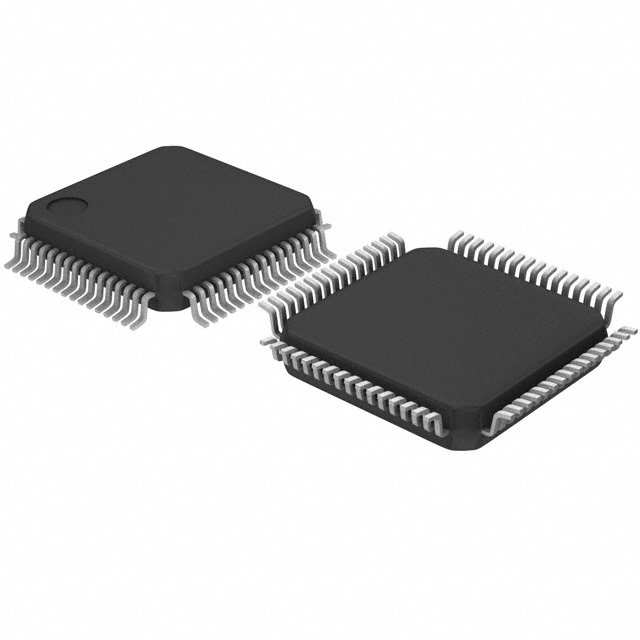
64-pin 10 × 10 STQFP
■
Pin compatible density upgrade to CY7C42X5V-ASC families
■
Pin compatible 3.3 V solutions for CY7C4255/75/85V
The CY7C4255/75/85V are high speed, low power, first-in
first-out (FIFO) memories with clocked read and write interfaces.
All are 18 bits wide and are pin and functionally compatible to the
CY7C42X5V Synchronous FIFO family. The CY7C4255/75/85V
can be cascaded to increase FIFO depth. Programmable
features include Almost Full/Almost Empty flags. These FIFOs
provide solutions for a wide variety of data buffering needs,
including high speed data acquisition, multiprocessor interfaces,
and communications buffering.
These FIFOs have 18-bit input and output ports that are
controlled by separate clock and enable signals. The input port
is controlled by a free-running clock (WCLK) and a write enable
pin (WEN).
When WEN is asserted, data is written into the FIFO on the rising
edge of the WCLK signal. While WEN is held active, data is
continually written into the FIFO on each cycle. The output port
is controlled in a similar manner by a free-running read clock
(RCLK) and a read enable pin (REN). In addition, the
CY7C4255/75/85V have an output enable pin (OE). The read
and write clocks may be tied together for single-clock operation
or the two clocks may be run independently for asynchronous
read or write applications. Clock frequencies up to 67 MHz are
achievable.
Retransmit and Synchronous Almost Full/Almost Empty flag
features are available on these devices.
Depth expansion is possible using the cascade input (WXI, RXI),
cascade output (WXO, RXO), and First Load (FL) pins. The
WXO and RXO pins are connected to the WXI and RXI pins of
the next device, and the WXO and RXO pins of the last device
must be connected to the WXI and RXI pins of the first device.
The FL pin of the first device is tied to VSS and the FL pin of all
the remaining devices must be tied to VCC.
For a complete list of related documentation, click here.
Selection Guide
Parameter
7C4255/75/85V-10
7C4255/75/85V-15
Maximum Frequency (MHz)
100
66.7
Maximum Access Time (ns)
8
10
Minimum Cycle Time (ns)
10
15
Minimum Data or Enable Setup (ns)
3.5
4
Minimum Data or Enable Hold (ns)
0
0
Maximum Flag Delay (ns)
8
10
30
30
Active Power Supply Current (ICC1) (mA)
Commercial
Industrial
Cypress Semiconductor Corporation
Document Number: 38-06012 Rev. *G
•
198 Champion Court
35
•
San Jose, CA 95134-1709
•
408-943-2600
Revised March 9, 2018
�CY7C4255V
CY7C4275V
CY7C4285V
Parameter
CY7C4255V
CY7C4275V
CY7C4285V
Density
8K × 18
32K × 18
64K × 18
Package
64-pin 10 × 10 TQFP
64-pin 10 × 10 TQFP
64-pin 10 × 10 TQFP
Logic Block Diagram
D0 – 17
INPUT
REGISTER
WCLK
WEN
FLAG
PROGRAM
REGISTER
WRITE
CONTROL
High
Density
Dual-Port
RAM Array
WRITE
POINTER
RS
FL/RT
WXI
WXO/HF
RXI
RXO
Document Number: 38-06012 Rev. *G
FLAG
LOGIC
8K x 18
32K x 18
64K x 18
FF
EF
PAE
PAF
SMODE
READ
POINTER
RESET
LOGIC
EXPANSION
LOGIC
THREE-ST ATE
OUTPUT REGISTER
Q0 – 17
READ
CONTROL
OE
RCLK
REN
Page 2 of 25
�CY7C4255V
CY7C4275V
CY7C4285V
Contents
Pin Configurations ........................................................... 4
Pin Definitions .................................................................. 5
Functional Overview ........................................................ 6
Architecture ...................................................................... 6
Resetting the FIFO ............................................................ 6
FIFO Operation ................................................................. 6
Programming .................................................................... 6
Flag Operation .................................................................. 6
Full Flag ....................................................................... 6
Empty Flag .................................................................. 6
Programmable Almost Empty/Almost Full Flag ........... 7
Retransmit ......................................................................... 7
Width Expansion Configuration ...................................... 7
Depth Expansion Configuration
(with Programmable Flags) ............................................. 8
Maximum Ratings ........................................................... 10
Operating Range ............................................................. 10
Electrical Characteristics ............................................... 10
Document Number: 38-06012 Rev. *G
Capacitance .................................................................... 11
AC Test Loads and Waveforms ..................................... 11
Switching Characteristics .............................................. 12
Switching Waveforms .................................................... 13
Ordering Information ...................................................... 21
Ordering Code Definitions ......................................... 21
Package Diagram ............................................................ 22
Acronyms ........................................................................ 23
Document Conventions ................................................. 23
Units of Measure ....................................................... 23
Document History Page ................................................. 24
Sales, Solutions, and Legal Information ...................... 25
Worldwide Sales and Design Support ....................... 25
Products .................................................................... 25
PSoC® Solutions ...................................................... 25
Cypress Developer Community ................................. 25
Technical Support ..................................................... 25
Page 3 of 25
�CY7C4255V
CY7C4275V
CY7C4285V
Pin Configurations
REN
LD
OE
RS
VCC
GND
EF
Q17
Q16
GND
Q15
VCC/SMODE
Figure 1. 64-pin STQFP pinout
CY7C4255V
CY7C4275V
Document Number: 38-06012 Rev. *G
48
47
46
45
44
43
42
41
40
39
38
37
36
35
34
33
Q14
Q13
GND
Q12
Q11
VCC
Q10
Q9
GND
Q8
Q7
Q6
Q5
GND
Q4
VCC
Q3
Q0
Q1
GND
Q2
17
18
19
20
21
22
23
24
25
26
27
28
29
30
31
32
CY7C4285V
PAE
1
2
3
4
5
6
7
8
9
10
11
12
13
14
15
16
FL/RT
WCLK
WEN
WXI
VCC
PAF
RXI
FF
WXO/HF
RXO
D15
D14
D13
D12
D11
D10
D9
D8
D7
D6
D5
D4
D3
D2
D1
D0
64
63
62
61
60
59
58
57
56
55
54
53
52
51
50
49
D16
D17
GND
RCLK
Top View
Page 4 of 25
�CY7C4255V
CY7C4275V
CY7C4285V
Pin Definitions
CY7C4255/75/85V 64-pin STQFP
Signal Name
Description
I/O
Function
D0–17
Data Inputs
I
Data inputs for an 18-bit bus.
Q0–17
Data Outputs
O
Data outputs for an 18-bit bus.
WEN
Write Enable
I
Enables the WCLK input.
REN
Read Enable
I
Enables the RCLK input.
WCLK
Write Clock
I
The rising edge clocks data into the FIFO when WEN is LOW and the FIFO is not Full.
When LD is asserted, WCLK writes data into the programmable flag-offset register.
RCLK
Read Clock
I
The rising edge clocks data out of the FIFO when REN is LOW and the FIFO is not
Empty. When LD is asserted, RCLK reads data out of the programmable flag-offset
register.
WXO/HF
Write Expansion
Out/Half Full Flag
O
Dual Mode Pin:
Single device or width expansion – Half Full status flag
Cascaded – Write Expansion Out signal, connected to WXI of next device
EF
Empty Flag
O
When EF is LOW, the FIFO is empty. EF is synchronized to RCLK.
FF
Full Flag
O
When FF is LOW, the FIFO is full. FF is synchronized to WCLK.
PAE
Programmable
Almost Empty
O
When PAE is LOW, the FIFO is almost empty based on the almost empty offset value
programmed into the FIFO. PAE is asynchronous when VCC/SMODE is tied to VCC.
It is synchronized to RCLK when VCC/SMODE is tied to VSS.
PAF
Programmable
Almost Full
O
When PAF is LOW, the FIFO is almost full based on the almost full offset value
programmed into the FIFO. PAF is asynchronous when VCC/SMODE is tied to VCC.
It is synchronized to WCLK when VCC/SMODE is tied to VSS.
LD
Load
I
When LD is LOW, D0–17 (Q0–17) are written (read) into (from) the
programmable-flag-offset register.
FL/RT
First Load/
Retransmit
I
Dual Mode Pin:
Cascaded – The first device in the daisy chain has FL tied to VSS; all other devices have
FL tied to VCC. In standard mode or width expansion, FL is tied to VSS on all devices.
Not Cascaded – Tied to VSS . Retransmit function is also available in standalone mode
by strobing RT.
WXI
Write Expansion
Input
I
Cascaded – Connected to WXO of previous device
Not Cascaded – Tied to VSS
RXI
Read Expansion
Input
I
Cascaded – Connected to RXO of previous device
Not Cascaded – Tied to VSS
RXO
Read Expansion
Output
O
Cascaded – Connected to RXI of next device
RS
Reset
I
Resets device to empty condition. A reset is required before an initial read or write
operation after power up.
OE
Output Enable
I
When OE is LOW, the FIFO’s data outputs drive the bus to which they are connected. If
OE is HIGH, the FIFO’s outputs are in High Z (high-impedance) state.
VCC/SMODE
Synchronous
Almost Empty/
Almost Full Flags
I
Dual Mode Pin:
Asynchronous Almost Empty/Almost Full flags – tied to VCC
Synchronous Almost Empty/Almost Full flags – tied to VSS
(Almost Empty synchronized to RCLK, Almost Full synchronized to WCLK.)
Document Number: 38-06012 Rev. *G
Page 5 of 25
�CY7C4255V
CY7C4275V
CY7C4285V
Functional Overview
Programming
The CY7C4255/75/85V provides five status pins. These pins are
decoded to determine one of five states: Empty, Almost Empty,
Half Full, Almost Full, and Full (see Table 2 on page 7). The Half
Full flag shares the WXO pin. This flag is valid in the standalone
and width expansion configurations. In the depth expansion, this
pin provides the expansion out (WXO) information that is used
to signal the next FIFO when it is to be activated.
The CY7C4255/75/85V devices contain two 16-bit offset
registers. Data present on D0–15 during a program write
determine the distance from Empty (Full) that the Almost Empty
(Almost Full) flags become active. If the user elects not to
program the FIFO’s flags, the default offset values are used (see
Table 2 on page 7). When the Load LD pin is set LOW and WEN
is set LOW, data on the inputs D0–15 is written into the Empty
offset register on the first LOW-to-HIGH transition of the write
clock (WCLK). When the LD pin and WEN are held LOW then
data is written into the Full offset register on the second
LOW-to-HIGH transition of the write clock (WCLK). The third
transition of the write clock (WCLK) again writes to the Empty
offset register (see Table 1). All offset registers do not have to be
written at one time. One or two offset registers can be written and
then, by bringing the LD pin HIGH, the FIFO is returned to normal
read/write operation. When the LD pin is set LOW, and WEN is
LOW, the next offset register in sequence is written.
The Empty and Full flags are synchronous, that is, they change
state relative to either the read clock (RCLK) or the write clock
(WCLK). When entering or exiting the Empty states, the flag is
updated exclusively by the RCLK. The flag denoting Full states
is updated exclusively by WCLK. The synchronous flag
architecture guarantees that the flags remain valid from one
clock cycle to the next. The Almost Empty/Almost Full flags
become synchronous if the VCC/SMODE is tied to VSS. All
configurations are fabricated using an advanced 0.35
CMOS technology. Input ESD protection is greater than
2001 V, and latch-up is prevented by the use of guard rings.
Architecture
The CY7C4255/75/85V consists of an array of 8K/32K/64K
words of 18 bits each (implemented by a dual port array of SRAM
cells), a read pointer, a write pointer, control signals (RCLK,
WCLK, REN, WEN, RS), and flags (EF, PAE, HF, PAF, FF). The
CY7C4255/75/85V also includes the control signals WXI, RXI,
WXO, RXO for depth expansion.
The contents of the offset registers can be read on the output
lines when the LD pin is set LOW and REN is set LOW. Then,
data can be read on the LOW-to-HIGH transition of the read
clock (RCLK).
Table 1. Write Offset Register
WCLK [1]
LD
WEN
0
0
Writing to offset registers:
Empty Offset
Full Offset
0
1
No Operation
1
0
Write Into FIFO
1
1
No Operation
Resetting the FIFO
Upon power up, the FIFO must be reset with a Reset (RS) cycle.
This causes the FIFO to enter the Empty condition signified by
EF being LOW. All data outputs go LOW after the falling edge of
RS only if OE is asserted. For the FIFO to reset to its default
state, the user must not read or write while RS is LOW.
FIFO Operation
When the WEN signal is active (LOW), data present on the D0–17
pins is written into the FIFO on each rising edge of the WCLK
signal. Similarly, when the REN signal is active LOW, data in the
FIFO memory is presented on the Q0–17 outputs. New data is
presented on each rising edge of RCLK while REN is active LOW
and OE is LOW. REN must set up tENS before RCLK for it to be
a valid read function. WEN must occur tENS before WCLK for it
to be a valid write function.
An output enable (OE) pin is provided to three-state the Q0–17
outputs when OE is deasserted. When OE is enabled (LOW),
data in the output register is available to the Q0–17 outputs after
tOE. If devices are cascaded, the OE function only outputs data
on the FIFO that is read enabled.
The FIFO contains overflow circuitry to disallow additional writes
when the FIFO is full, and under flow circuitry to disallow
additional reads when the FIFO is empty. An empty FIFO
maintains the data of the last valid read on its Q0–17 outputs even
after additional reads occur.
Selection
Flag Operation
The CY7C4255/75/85V devices provide five flag pins to indicate
the condition of the FIFO contents. Empty and Full are
synchronous. PAE and PAF are synchronous if VCC/SMODE is
tied to VSS.
Full Flag
The Full Flag (FF) goes LOW when device is Full. Write
operations are inhibited whenever FF is LOW regardless of the
state of WEN. FF is synchronized to WCLK, that is, it is
exclusively updated by each rising edge of WCLK.
Empty Flag
The Empty Flag (EF) goes LOW when the device is empty. Read
operations are inhibited whenever EF is LOW, regardless of the
state of REN. EF is synchronized to RCLK, that is, it is
exclusively updated by each rising edge of RCLK.
Note
1. The same selection sequence applies to reading from the registers. REN is enabled and read is performed on the LOW-to-HIGH transition of RCLK.
Document Number: 38-06012 Rev. *G
Page 6 of 25
�CY7C4255V
CY7C4275V
CY7C4285V
Programmable Almost Empty/Almost Full Flag
been programmed, the PAF or PAE is asserted, signifying that
the FIFO is either Almost Full or Almost Empty. See Table 2 for
a description of programmable flags.
The CY7C4255/75/85V features programmable Almost Empty
and Almost Full Flags. Each flag can be programmed (described
in section Programming on page 6) a specific distance from the
corresponding boundary flags (Empty or Full). When the FIFO
contains the number of words or fewer for which the flags have
When the SMODE pin is tied LOW, the PAF flag signal transition
is caused by the rising edge of the write clock and the PAE flag
transition is caused by the rising edge of the read clock.
Table 2. Flag Truth Table
Number of Words in FIFO
7C4255V – 8K × 18
0
1 to n
7C4275V – 32K × 18
0
[2]
1 to n
7C4285V – 64K × 18
0
[2]
1 to n
[2]
FF
PAF
HF
PAE
EF
H
H
H
L
L
H
H
H
L
H
(n + 1) to 4096
(n + 1) to 16384
(n + 1) to 32768
H
H
H
H
H
4097 to (8192 – (m + 1))
16385 to (32768 – (m + 1))
32769 to (65536 – (m + 1))
H
H
L
H
H
(8192 – m) [3] to 8192
(32768 – m) [3] to 32767
(65536 – m) [3] to 65535
H
L
L
H
H
8192
32768
65536
L
L
L
H
H
Retransmit
Width Expansion Configuration
The retransmit feature is beneficial when transferring packets of
data. It enables the receipt of data to be acknowledged by the
receiver and retransmitted if necessary.
The CY7C4255/75/85V can be expanded in width to provide
word widths greater than 18 in increments of 18. During width
expansion mode, all control line inputs are common and all flags
are available. Empty (Full) flags must be created by ANDing the
Empty (Full) flags of every FIFO. The PAE and PAF flags can be
detected from any one device. This technique avoids reading
data from, or writing data to the FIFO that is “staggered” by one
clock cycle due to the variations in skew between RCLK and
WCLK. Figure 2 on page 8 demonstrates a 36-word width by
using two CY7C4255/75/85Vs.
The Retransmit (RT) input is active in the standalone and width
expansion modes. The retransmit feature is intended for use
when a number of writes equal to or less than the depth of the
FIFO have occurred and at least one word has been read since
the last RS cycle. A HIGH pulse on RT resets the internal read
pointer to the first physical location of the FIFO. WCLK and
RCLK may be free running but must be disabled during and tRTR
after the retransmit pulse. With every valid read cycle after
retransmit, previously accessed data is read and the read pointer
is incremented until it is equal to the write pointer. Flags are
governed by the relative locations of the read and write pointers
and are updated during a retransmit cycle. Data written to the
FIFO after activation of RT are transmitted also. The full depth of
the FIFO can be repeatedly retransmitted.
Notes
2. n = Empty Offset (Default Values: CY7C4255/75/85V n = 127).
3. m = Full Offset (Default Values: CY7C4255/75/85V n = 127).
Document Number: 38-06012 Rev. *G
Page 7 of 25
�CY7C4255V
CY7C4275V
CY7C4285V
Figure 2. Block Diagram of 8K/32K/64K × 18 Low Voltage Synchronous FIFO Memory in Width Expansion Configuration
RESET (RS)
DATA IN (D) 36
RESET (RS)
18
18
READ CLOCK (RCLK)
WRITE CLOCK (WCLK)
READ ENABLE (REN)
WRITE ENABLE (WEN)
OUTPUT ENABLE (OE)
LOAD (LD)
PROGRAMMABLE(PAE)
7C4255V
7C4255V
HALF FULL FLAG (HF)
7C4275V
7C4275V
7C4285V
7C4285V
FF
FF
EF
PROGRAMMABLE (PAF)
EMPTY FLAG (EF)
EF
18
FULL FLAG (FF)
DATA OUT (Q)
36
18
FIRST LOAD (FL)
WRITE EXPANSION IN (WXI)
READ EXPANSION IN (RXI)
4275V–24
Depth Expansion Configuration (with Programmable Flags)
The CY7C4255/75/85V can easily be adapted to applications requiring more than 8 K/32 K/64 K words of buffering.
Figure 3 on page 9 shows Depth Expansion using three CY7C4255/75/85Vs. Maximum depth is limited only by signal loading. Follow
these steps:
1. The first device must be designated by grounding the First Load (FL) control input.
2. All other devices must have FL in the HIGH state.
3. The Write Expansion Out (WXO) pin of each device must be tied to the Write Expansion In (WXI) pin of the next device.
4. The Read Expansion Out (RXO) pin of each device must be tied to the Read Expansion In (RXI) pin of the next device.
5. All Load (LD) pins are tied together.
6. The Half Full Flag (HF) is not available in the Depth Expansion Configuration.
7. EF, FF, PAE, and PAF are created with composite flags by ORing together these respective flags for monitoring. The composite
PAE and PAF flags are not precise.
Document Number: 38-06012 Rev. *G
Page 8 of 25
�CY7C4255V
CY7C4275V
CY7C4285V
Figure 3. Block Diagram of 8K/32K/64K × 18 Low Voltage Synchronous FIFO Memory with Programmable Flags in
Depth Expansion Configuration
WXO RXO
7C4255V
7C4275V
7C4285V
VCC
FL
FF
EF
PAE
PAF
WXI RXI
WXO RXO
7C4255V
DATA IN (D)
DATA OUT (Q)
7C4275V
7C4285V
VCC
FL
FF
EF
PAF
PAE
WXI RXI
WRITE CLOCK (WCLK)
WXO RXO
WRITE ENABLE (WEN)
READ ENABLE (REN)
7C4255V
RESET (RS)
READ CLOCK (RCLK)
OUTPUT ENABLE (OE)
7C4275V
7C4285V
LOAD (LD)
FF
FF
PAF
EF
EF
PAFWXI RXI PAE
PAE
FIRST LOAD (FL)
4275V–25
Document Number: 38-06012 Rev. *G
Page 9 of 25
�CY7C4255V
CY7C4275V
CY7C4285V
Maximum Ratings
Output Current into Outputs (LOW) ............................ 20 mA
Exceeding maximum ratings [4] may impair the useful life of the
device. These user guidelines are not tested.
Storage Temperature .............................. –65 °C to +150 °C
Static Discharge Voltage
(per MIL-STD-883, Method 3015) .......................... > 2001 V
Latch-Up Current ................................................... > 200 mA
Operating Range
Ambient Temperature with
Power Applied ........................................ –55 °C to +125 °C
Range
Supply Voltage to Ground Potential .... –0.5 V to VCC + 0.5 V
Commercial
DC Voltage Applied to Outputs
in High Z State .................................... –0.5 V to VCC + 0.5 V
Industrial
VCC[5]
Ambient Temperature
[6]
0 °C to +70 °C
3.3 V ± 300 mV
–40 °C to +85 °C
3.3 V ± 300 mV
DC Input Voltage 0.5 V to VCC + 0.5 V
Electrical Characteristics
Over the Operating Range
Parameter [7]
Description
Test Conditions
7C4255/85V-10
7C4255/75/85V-15
Unit
Min
Max
Min
Max
2.4
–
2.4
–
V
–
0.4
–
0.4
V
VOH
Output HIGH Voltage
VCC = Min,
IOH = –1.0 mA;
VCC = 3.0 V,
IOH = –2.0 mA
VOL
Output LOW Voltage
VCC = Min,
IOL = 4.0 mA;
VCC = 3.0 V,
IOL = 8.0 mA
VIH[8]
Input HIGH Voltage
2.0
VCC
2.0
VCC
V
[8]
Input LOW Voltage
–0.5
0.8
–0.5
0.8
V
VIL
IIX
Input Leakage Current
VCC = Max
–10
+10
–10
+10
A
IOZL
IOZH
Output OFF, High Z Current
OE > VIH,
VSS < VO < VCC
–10
+10
–10
+10
A
ICC1[9]
Active Power Supply Current
Commercial
–
30
–
30
mA
Industrial
–
–
–
35
mA
Commercial
–
4
–
4
mA
Industrial
–
–
–
4
mA
ISB[10]
Average Standby Current
Notes
4. The Voltage on any input or IO pin cannot exceed the power pin during power-up.
5. VCC range for commercial –10 ns is 3.3 V ± 150 mV.
6. TA is the “instant on” case temperature.
7. See the last page of this specification for Group A subgroup testing information.
8. The VIH and V IL specifications apply for all inputs except WXI, RXI. The WXI, RXI pin is not a TTL input. It is connected to either RXO, WXO of the previous
device or VSS.
9. Input signals switch from 0 V to 3 V with a rise/fall time of less than 3 ns, clocks and clock enables switch at 20 MHz, while data inputs switch at 10 MHz. Outputs
are unloaded.
10. All inputs = VCC – 0.2 V, except RCLK and WCLK (which are at frequency = 0 MHz), and FL/RT which is at VSS. All outputs are unloaded.
Document Number: 38-06012 Rev. *G
Page 10 of 25
�CY7C4255V
CY7C4275V
CY7C4285V
Capacitance
Parameter [11]
Description
CIN
Input capacitance
COUT
Output capacitance
Test Conditions
TA = 25 °C, f = 1 MHz, VCC = 3.3 V
Max
Unit
5
pF
7
pF
AC Test Loads and Waveforms
Figure 4. AC Test Loads and Waveforms (-15) [12, 13]
R1 = 330
ALL INPUT PULSES
3.3 V
OUTPUT
3.0 V
R2 = 510
CL
90%
10%
GND
90%
10%
3 ns
INCLUDING
JIG AND
SCOPE
4275V–4
Equivalent to:
3 ns
THÉVENIN EQUIVALENT
200
OUTPUT
4287V–5
2.0 V
Figure 5. AC Test Loads and Waveforms (-10)
ALL INPUT PULSES
VCC/2
3.0 V
50
I/O
GND
3 ns
Z0 = 50
4275V–6
90%
10%
90%
10%
3 ns
4275V–7
Notes
11. Tested initially and after any design changes that may affect these parameters.
12. CL = 30 pF for all AC parameters except for tOHZ.
13. CL = 5 pF for tOHZ.
Document Number: 38-06012 Rev. *G
Page 11 of 25
�CY7C4255V
CY7C4275V
CY7C4285V
Switching Characteristics
Over the Operating Range
Parameter
7C4255/85V-10
Description
7C4255/75/85V-15
Unit
Min
Max
Min
Max
–
100
–
66.7
MHz
tS
Clock Cycle Frequency
tA
Data Access Time
2
8
2
10
ns
tCLK
Clock Cycle Time
10
–
15
–
ns
tCLKH
Clock HIGH Time
4.5
–
6
–
ns
tCLKL
Clock LOW Time
4.5
–
6
–
ns
tDS
Data Setup Time
3.5
–
4
–
ns
tDH
Data Hold Time
0
–
0
–
ns
tENS
Enable Setup Time
3.5
–
4
–
ns
tENH
Enable Hold Time
0
–
0
–
ns
10
–
15
–
ns
8
–
10
–
ns
[14]
tRS
Reset Pulse Width
tRSR
Reset Recovery Time
tRSF
Reset to Flag and Output Time
–
10
–
15
ns
tPRT
Retransmit Pulse Width
60
–
60
–
ns
tRTR
Retransmit Recovery Time
90
–
90
–
ns
0
–
0
–
ns
3
7
3
10
ns
3
7
3
8
ns
tOLZ
Output Enable to Output in Low Z
tOE
Output Enable to Output Valid
[15]
tOHZ
Output Enable to Output in High
tWFF
Write Clock to Full Flag
–
8
–
10
ns
tREF
Read Clock to Empty Flag
–
8
–
10
ns
Z[15]
[16]
tPAFasynch
Clock to Programmable Almost Full Flag
(Asynchronous mode, VCC/SMODE tied to VCC)
–
15
–
16
ns
tPAFsynch
Clock to Programmable Almost Full Flag
(Synchronous mode, VCC/SMODE tied to VSS)
–
8
–
10
ns
tPAEasynch
Clock to Programmable Almost Empty Flag [16]
(Asynchronous mode, VCC/SMODE tied to VCC)
–
15
–
16
ns
tPAEsynch
Clock to Programmable Almost Full Flag
(Synchronous mode, VCC/SMODE tied to VSS)
–
8
–
10
ns
tHF
Clock to Half Full Flag
–
12
–
16
ns
tXO
Clock to Expansion Out
–
6
–
10
ns
tXI
Expansion in Pulse Width
4.5
–
6.5
–
ns
tXIS
Expansion in Setup Time
4
–
5
–
ns
tSKEW1
Skew Time between Read Clock and Write Clock for Full
Flag
5
–
6
–
ns
tSKEW2
Skew Time between Read Clock and Write Clock for
Empty Flag
5
–
6
–
ns
tSKEW3
Skew Time between Read Clock and Write Clock for
Programmable Almost Empty and Programmable Almost
Full Flags (Synchronous Mode only)
10
–
15
–
ns
Notes
14. Pulse widths less than minimum values are not allowed.
15. Values guaranteed by design, not currently tested.
16. tPAFasynch, tPAEasynch, after program register write are valid until 5 ns + tPAF(E).
Document Number: 38-06012 Rev. *G
Page 12 of 25
�CY7C4255V
CY7C4275V
CY7C4285V
Switching Waveforms
Figure 6. Write Cycle Timing
tCLK
tCLKH
tCLKL
WCLK
tDS
tDH
D0 –D17
tENS
tENH
WEN
NO OPERATION
tWFF
tWFF
FF
tSKEW1
[17]
RCLK
REN
Figure 7. Read Cycle Timing
tCLK
tCLKH
tCLKL
RCLK
tENS
tENH
REN
NO OPERATION
tREF
tREF
EF
tA
Q0 –Q17
VALID DATA
tOLZ
tOHZ
tOE
OE
tSKEW2[18]
WCLK
WEN
Notes
17. tSKEW1 is the minimum time between a rising RCLK edge and a rising WCLK edge to guarantee that FF goes HIGH during the current clock cycle. If the time between
the rising edge of RCLK and the rising edge of WCLK is less than tSKEW1, then FF may not change state until the next WCLK rising edge.
18. tSKEW2 is the minimum time between a rising WCLK edge and a rising RCLK edge to guarantee that EF goes HIGH during the current clock cycle. If the time between
the rising edge of WCLK and the rising edge of RCLK is less than tSKEW2, then EF may not change state until the next RCLK rising edge.
Document Number: 38-06012 Rev. *G
Page 13 of 25
�CY7C4255V
CY7C4275V
CY7C4285V
Switching Waveforms (continued)
Figure 8. Reset Timing [19]
tRS
RS
tRSR
REN, WEN,
LD
tRSF
EF,PAE
tRSF
FF,PAF,
HF
tRSF
[20]
OE=1
Q0 – Q17
OE=0
Figure 9. First Data Word Latency after Reset with Simultaneous Read and Write
WCLK
tDS
D0 –D17
D0 (FIRSTVALID WRITE)
D1
tENS
D2
D3
D4
[21]
tFRL
WEN
tSKEW2
RCLK
tREF
EF
REN
tA
Q0 –Q17
tA
D0
tOLZ
[22]
D1
tOE
OE
Notes
19. The clocks (RCLK, WCLK) can be free-running during reset.
20. After reset, the outputs are LOW if OE = 0 and three-state if OE = 1.
21. When tSKEW2 > minimum specification, tFRL (maximum) = tCLK + tSKEW2. When tSKEW2 < minimum specification, tFRL (maximum) = either 2 × tCLK + tSKEW2 or
tCLK + tSKEW2. The Latency Timing applies only at the Empty Boundary (EF = LOW).
22. The first word is always available the cycle after EF goes HIGH.
Document Number: 38-06012 Rev. *G
Page 14 of 25
�CY7C4255V
CY7C4275V
CY7C4285V
Switching Waveforms (continued)
Figure 10. Empty Flag Timing
WCLK
tDS
tDS
D0
D0 –D17
D1
tENH
tENS
tENH
tENS
WEN
[23]
[23]
tFRL
tFRL
RCLK
tREF
tSKEW2
tREF
tREF
tSKEW2
EF
REN
OE
tA
D0
Q0 –Q17
Figure 11. Full Flag Timing
NO WRITE
NO WRITE
WCLK
tSKEW1
[24]
tDS
tSKEW1
[24]
DATA WRITE
DATA WRITE
D0 –D17
tWFF
tWFF
tWFF
FF
WEN
RCLK
tENS
tENH
tENS
tENH
REN
OE
LOW
tA
Q0 –Q17
DATA IN OUTPUT REGISTER
tA
DATA READ
NEXT DATA READ
Notes
23. When tSKEW2 > minimum specification, tFRL (maximum) = tCLK + tSKEW2. When tSKEW2 < minimum specification, tFRL (maximum) = either 2 × tCLK + tSKEW2 or
tCLK + tSKEW2. The Latency Timing applies only at the Empty Boundary (EF = LOW).
24. tSKEW1 is the minimum time between a rising RCLK edge and a rising WCLK edge to guarantee that FF goes HIGH during the current clock cycle. If the time between
the rising edge of RCLK and the rising edge of WCLK is less than tSKEW1, then FF may not change state until the next WCLK rising edge.
Document Number: 38-06012 Rev. *G
Page 15 of 25
�CY7C4255V
CY7C4275V
CY7C4285V
Switching Waveforms (continued)
Figure 12. Half Full Timing
tCLKH
tCLKL
WCLK
tENS tENH
WEN
tHF
HF
HALF FULL + 1
OR MORE
HALF FULL OR LESS
HALF FULL OR LESS
tHF
RCLK
tENS
REN
Figure 13. Programmable Almost Empty Flag Timing
tCLKH
tCLKL
WCLK
tENS tENH
WEN
tPAE
PAE
[25]
N + 1 WORDS
IN FIFO
tPAE
n WORDS IN FIFO
RCLK
tENS
REN
Note
25. PAE is offset = n. Number of data words into FIFO already = n.
Document Number: 38-06012 Rev. *G
Page 16 of 25
�CY7C4255V
CY7C4275V
CY7C4285V
Switching Waveforms (continued)
Figure 14. Programmable Almost Empty Flag Timing (applies only in SMODE (SMODE is LOW))
tCLKL
tCLKH
WCLK
tENS tENH
WEN
Note 26
PAE
tSKEW3
N + 1 WORDS
IN FIFO
[27]
tPAE synch
Note 28
tPAE synch
RCLK
tENS
tENS tENH
REN
Figure 15. Programmable Almost Full Flag Timing
tCLKH
tCLKL
Note 26
WCLK
tENS tENH
WEN
PAF
[29]
tPAF
FULL– M WORDS
IN FIFO [30]
tPAF
FULL– (M+1) WORDS
IN FIFO [31]
RCLK
tENS
REN
Notes
26. PAF offset = m. Number of data words written into FIFO already = 8192 (m + 1) for the CY7C4255V, 32768 (m + 1) for the CY7C4275V, and 65536 (m + 1) for
the CY7C4285V.
27. tSKEW3 is the minimum time between a rising WCLK and a rising RCLK edge for PAE to change state during that clock cycle. If the time between the edge of WCLK
and the rising RCLK is less than tSKEW3, then PAE may not change state until the next RCLK.
28. If a read is performed on this rising edge of the read clock, there are Empty + (n1) words in the FIFO when PAE goes LOW.
29. PAF is offset = m.
30. 8192 m words in CY7C4255V, 32768m words in CY7C4275V, and 65536 m words in CY7C4285V.
31. 8192 (m + 1) words in CY7C4255V, 32768 (m + 1) words in CY7C4275V, and 65536 (m + 1) words in CY7C4285V.
Document Number: 38-06012 Rev. *G
Page 17 of 25
�CY7C4255V
CY7C4275V
CY7C4285V
Switching Waveforms (continued)
Figure 16. Programmable Almost Full Flag Timing (applies only in SMODE (SMODE is LOW))
Note 32
tCLKL
tCLKH
WCLK
tENS tENH
WEN
tPAF
PAF
FULL– M WORDS
IN FIFO [33]
FULL – M + 1 WORDS
IN FIFO
[34]
tSKEW3
tPAF synch
RCLK
tENS
tENS tENH
REN
Figure 17. Write Programmable Registers
tCLK
tCLKL
tCLKH
WCLK
tENS
tENH
LD
tENS
WEN
tDS
tDH
PAE OFFSET
D0 –D17
PAE OFFSET
PAF OFFSET
D0 – D11
Notes
32. If a write is performed on this rising edge of the write clock, there are Full (m1) words of the FIFO when PAF goes LOW.
33. 8192 m words in CY7C4255V, 32768m words in CY7C4275V, and 65536 m words in CY7C4285V.
34. tSKEW3 is the minimum time between a rising RCLK and a rising WCLK edge for PAF to change state during that clock cycle. If the time between the edge of RCLK
and the rising edge of WCLK is less than tSKEW3, then PAF may not change state until the next WCLK rising edge.
Document Number: 38-06012 Rev. *G
Page 18 of 25
�CY7C4255V
CY7C4275V
CY7C4285V
Switching Waveforms (continued)
Figure 18. Read Programmable Registers
tCLK
tCLKL
tCLKH
RCLK
tENS
tENH
LD
tENS
WEN
tA
UNKNOWN
Q0 –Q17
PAE OFFSET
PAF OFFSET
PAE OFFSET
Figure 19. Write Expansion Out Timing
tCLKH
WCLK
35
tXO
36
WXO
tXO
tENS
WEN
Figure 20. Read Expansion Out Timing
tCLKH
WCLK
35
tXO
RXO
tXO
tENS
REN
Figure 21. Write Expansion In Timing
tXI
WXI
WCLK
tXIS
Notes
35. Read from Last Physical Location.
36. Write to Last Physical Location.
Document Number: 38-06012 Rev. *G
Page 19 of 25
�CY7C4255V
CY7C4275V
CY7C4285V
Switching Waveforms (continued)
Figure 22. Read Expansion In Timing
tXI
RXI
tXIS
RCLK
Figure 23. Retransmit Timing [37, 38, 39]
FL/RT
tPRT
tRTR
REN/WEN
EF/FF
and all
async flags
HF/PAE/PAF
Notes
37. Clocks are free-running in this case.
38. The flags may change state during Retransmit as a result of the offset of the read and write pointers, but flags are valid at tRTR.
39. For the synchronous PAE and PAF flags (SMODE), an appropriate clock cycle is necessary after tRTR to update these flags.
Document Number: 38-06012 Rev. *G
Page 20 of 25
�CY7C4255V
CY7C4275V
CY7C4285V
Ordering Information
Speed
(ns)
Ordering Code
Package
Diagram
Package Type
Operating
Range
8K × 18 Low-Voltage Deep Sync FIFO
10
CY7C4255V-10ASXC
51-85051 64-pin TQFP (10 × 10 × 1.4 mm) Pb-free
Commercial
15
CY7C4255V-15ASXC
51-85051 64-pin TQFP (10 × 10 × 1.4 mm) Pb-free
Commercial
51-85051 64-pin TQFP (10 × 10 × 1.4 mm) Pb-free
Commercial
32K × 18 Low-Voltage Deep Sync FIFO
15
CY7C4275V-15ASXC
64K × 18 Low-Voltage Deep Sync FIFO
10
CY7C4285V-10ASXC
51-85051 64-pin TQFP (10 × 10 × 1.4 mm) Pb-free
Commercial
15
CY7C4285V-15ASXC
51-85051 64-pin TQFP (10 × 10 × 1.4 mm) Pb-free
Commercial
CY7C4285V-15ASC
CY7C4285V-15ASXI
64-pin TQFP (10 × 10 × 1.4 mm)
51-85051 64-pin TQFP (10 × 10 × 1.4 mm) Pb-free
Industrial
Ordering Code Definitions
CY 7C 4 2X 5
V - XX AS X X
Temperature Range: X = C or I
C = Commercial; I = Industrial
X = Pb-free (RoHS Compliant)
Package Type: AS = STQFP
Speed: XX = 10 ns or 15 ns
V = 3.3 V
Width: 5 = ×18
Depth: 2X = 25 or 27 or 28
25 = 8Kb; 27 = 32Kb; 28 = 64Kb
FIFO
7C = Dual Port
Company ID: CY = Cypress
Document Number: 38-06012 Rev. *G
Page 21 of 25
�CY7C4255V
CY7C4275V
CY7C4285V
Package Diagram
Figure 24. 64-pin TQFP (10 × 10 × 1.4 mm) Package Outline, 51-85051
51-85051 *D
Document Number: 38-06012 Rev. *G
Page 22 of 25
�CY7C4255V
CY7C4275V
CY7C4285V
Acronyms
Acronym
Document Conventions
Description
Units of Measure
CMOS
Complementary Metal Oxide Semiconductor
FIFO
First-In First-Out
°C
degree Celsius
I/O
Input/Output
MHz
megahertz
OE
Output Enable
µA
microampere
REN
Read Enable
mA
milliampere
RCLK
Read Clock
ms
millisecond
RT
Retransmit
mV
millivolt
RS
Reset
ns
nanosecond
TQFP
Thin Quad Flat Pack
pF
picofarad
WCLK
Write Clock
V
volt
WEN
Write Enable
W
watt
Document Number: 38-06012 Rev. *G
Symbol
Unit of Measure
Page 23 of 25
�CY7C4255V
CY7C4275V
CY7C4285V
Document History Page
Document Title: CY7C4255V/CY7C4275V/CY7C4285V, 8K/32K/64K × 18 Low Voltage Deep Sync FIFOs
Document Number: 38-06012
Rev.
ECN
Orig. of
Change
Submission
Date
**
106473
SZV
09/10/2001
Changed spec number from 38-00654 to 38-06012.
*A
122264
RBI
12/26/2002
Updated Maximum Ratings:
Added Note 4 and referred the same note in maximum ratings.
*B
2556036
VKN /
AESA
08/22/2008
Updated Ordering Information:
Updated part numbers.
Updated to new template.
*C
2896039
RAME
03/19/2010
Updated Ordering Information:
Updated part numbers.
Updated Package Diagram:
spec 51-85051 – Changed revision from *A to *B.
Updated to new template.
*D
3123000
ADMU
12/31/2010
Removed 25 ns speed bin related information in all instances across the
document.
Updated Ordering Information:
No change in part numbers.
Added Ordering Code Definitions.
Added Acronyms and Units of Measure.
Updated to new template.
*E
4234281
ADMU
01/06/2014
Updated Document Title to read as “CY7C4255V/CY7C4275V/CY7C4285V,
8K/32K/64K × 18 Low Voltage Deep Sync FIFOs”.
Removed CY7C4265V related information across the document.
Updated Ordering Information:
Updated part numbers.
Updated Package Diagram:
spec 51-85051 – Changed revision from *B to *C.
Updated to new template.
*F
4575241
ADMU
11/19/2014
Updated Functional Description:
Added “For a complete list of related documentation, click here.” at the end.
*G
6093642
VINI
03/09/2018
Updated Ordering Information:
Updated part numbers.
Updated Package Diagram:
spec 51-85051 – Changed revision from *C to *D.
Updated to new template.
Document Number: 38-06012 Rev. *G
Description of Change
Page 24 of 25
�CY7C4255V
CY7C4275V
CY7C4285V
Sales, Solutions, and Legal Information
Worldwide Sales and Design Support
Cypress maintains a worldwide network of offices, solution centers, manufacturer’s representatives, and distributors. To find the office
closest to you, visit us at Cypress Locations.
PSoC® Solutions
Products
Arm® Cortex® Microcontrollers
Automotive
cypress.com/arm
cypress.com/automotive
Clocks & Buffers
Interface
Internet of Things
Memory
cypress.com/clocks
cypress.com/interface
cypress.com/iot
cypress.com/memory
Microcontrollers
cypress.com/mcu
PSoC
cypress.com/psoc
Power Management ICs
Touch Sensing
USB Controllers
Wireless Connectivity
PSoC 1 | PSoC 3 | PSoC 4 | PSoC 5LP | PSoC 6 MCU
Cypress Developer Community
Community | Projects | Video | Blogs | Training | Components
Technical Support
cypress.com/support
cypress.com/pmic
cypress.com/touch
cypress.com/usb
cypress.com/wireless
© Cypress Semiconductor Corporation, 2001-2018. This document is the property of Cypress Semiconductor Corporation and its subsidiaries, including Spansion LLC ("Cypress"). This document,
including any software or firmware included or referenced in this document ("Software"), is owned by Cypress under the intellectual property laws and treaties of the United States and other countries
worldwide. Cypress reserves all rights under such laws and treaties and does not, except as specifically stated in this paragraph, grant any license under its patents, copyrights, trademarks, or other
intellectual property rights. If the Software is not accompanied by a license agreement and you do not otherwise have a written agreement with Cypress governing the use of the Software, then Cypress
hereby grants you a personal, non-exclusive, nontransferable license (without the right to sublicense) (1) under its copyright rights in the Software (a) for Software provided in source code form, to
modify and reproduce the Software solely for use with Cypress hardware products, only internally within your organization, and (b) to distribute the Software in binary code form externally to end users
(either directly or indirectly through resellers and distributors), solely for use on Cypress hardware product units, and (2) under those claims of Cypress's patents that are infringed by the Software (as
provided by Cypress, unmodified) to make, use, distribute, and import the Software solely for use with Cypress hardware products. Any other use, reproduction, modification, translation, or compilation
of the Software is prohibited.
TO THE EXTENT PERMITTED BY APPLICABLE LAW, CYPRESS MAKES NO WARRANTY OF ANY KIND, EXPRESS OR IMPLIED, WITH REGARD TO THIS DOCUMENT OR ANY SOFTWARE
OR ACCOMPANYING HARDWARE, INCLUDING, BUT NOT LIMITED TO, THE IMPLIED WARRANTIES OF MERCHANTABILITY AND FITNESS FOR A PARTICULAR PURPOSE. To the extent
permitted by applicable law, Cypress reserves the right to make changes to this document without further notice. Cypress does not assume any liability arising out of the application or use of any
product or circuit described in this document. Any information provided in this document, including any sample design information or programming code, is provided only for reference purposes. It is
the responsibility of the user of this document to properly design, program, and test the functionality and safety of any application made of this information and any resulting product. Cypress products
are not designed, intended, or authorized for use as critical components in systems designed or intended for the operation of weapons, weapons systems, nuclear installations, life-support devices or
systems, other medical devices or systems (including resuscitation equipment and surgical implants), pollution control or hazardous substances management, or other uses where the failure of the
device or system could cause personal injury, death, or property damage ("Unintended Uses"). A critical component is any component of a device or system whose failure to perform can be reasonably
expected to cause the failure of the device or system, or to affect its safety or effectiveness. Cypress is not liable, in whole or in part, and you shall and hereby do release Cypress from any claim,
damage, or other liability arising from or related to all Unintended Uses of Cypress products. You shall indemnify and hold Cypress harmless from and against all claims, costs, damages, and other
liabilities, including claims for personal injury or death, arising from or related to any Unintended Uses of Cypress products.
Cypress, the Cypress logo, Spansion, the Spansion logo, and combinations thereof, WICED, PSoC, CapSense, EZ-USB, F-RAM, and Traveo are trademarks or registered trademarks of Cypress in
the United States and other countries. For a more complete list of Cypress trademarks, visit cypress.com. Other names and brands may be claimed as property of their respective owners.
Document Number: 38-06012 Rev. *G
Revised March 9, 2018
Page 25 of 25
�