PRELIMINARY
CY7C60445, CY7C6045x
enCoRe™ V Low Voltage Microcontroller
Features
■
Powerful Harvard Architecture Processor ❐ M8C processor speeds running up to 24 MHz ❐ Low power at high processing speeds ❐ Interrupt controller ❐ 1.71V to 3.6V operating voltage ❐ Temperature range: 0°C to 70°C Flexible On-Chip Memory ❐ Up to 32K Flash program storage 50,000 Erase/write cycles ❐ Up to 2048 bytes SRAM data storage ❐ Flexible protection modes ❐ In-System Serial Programming (ISSP) Complete Development Tools ❐ Free development tool (PSoC Designer™) ❐ Full featured, in-circuit emulator and programmer ❐ Full speed emulation ❐ Complex breakpoint structure ❐ 128K trace memory Precision, Programmable Clocking ❐ Crystal-less oscillator with support for an external crystal or resonator ❐ Internal ±5.0% 6, 12, or 24 MHz main oscillator ❐ Internal low speed oscillator at 32 kHz for watchdog and sleep.The frequency range is 19–50 kHz with a 32 kHz typical value
■
■
Programmable Pin Configurations ❐ 25 mA sink current on all GPIO ❐ Pull up, high Z, open drain, CMOS drive modes on all GPIO ❐ Configurable inputs on all GPIO ❐ Low dropout voltage regulator for Port1 pins. Programmable to output 3.0, 2.5, or 1.8V at the I/O pins ❐ Selectable, regulated digital IO on Port 1 • Configurable input threshold for Port 1 • 3.0V, 20 mA total Port 1 source current • Hot-swappable ❐ 5 mA strong drive mode on Ports 0 and 1 Additional System Resources ❐ Configurable communication speeds 2 ❐ I C™ Slave • Selectable to 50 kHz, 100 kHz, or 400 kHz • Implementation requires no clock stretching • Implementation during sleep modes with less than 100 mA • Hardware address detection ❐ SPI master and SPI slave • Configurable between 46.9 kHz and 3 MHz ❐ Three 16-bit timers ❐ 10-bit ADC for monitoring battery voltage or other signals ❐ Watchdog and sleep timers ❐ Integrated supervisory circuit
■
■
■
enCoRe V LV Block Diagram
enCoRe V Low Voltage CORE
Port 4 Port 3 Port 2 Port 1 Port 0 Prog. LDO
System Bus
SRAM 2048 Bytes Interrupt Controller SROM Flash 32K Sleep and Watchdog
CPU Core (M8C)
6/12/24 MHz Internal Main Oscillator
3 16-Bit Timers
I2C Slave/SPI Master-Slave
POR and LVD System Resets
SYSTEM RESOURCES
Cypress Semiconductor Corporation Document Number: 001-12395 Rev. *F
•
198 Champion Court
•
San Jose, CA 95134-1709 • 408-943-2600 Revised March 19, 2008
[+] Feedback
�PRELIMINARY
CY7C60445, CY7C6045x
Functional Overview
The enCoRe V LV family of devices are designed to replace multiple traditional low voltage microcontroller system components with one, low cost single chip programmable component. Communication peripherals (I2C/SPI), a fast CPU, Flash program memory, SRAM data memory, and configurable IO are included in a range of convenient pinouts. The architecture for this device family, as illustrated in enCoRe V LV Block Diagram, is comprised of two main areas: the CPU core and the system resources. Depending on the enCoRe V LV package, up to 36 general purpose IO (GPIO) are also included. Enhancements over the Cypress’ legacy low voltage microcontrollers include faster CPU at lower voltage operation, lower current consumption, twice the RAM and Flash, hot-swapable IOs, I2C hardware address recognition, new very low current sleep mode, and new package options.
■
Low Voltage Detection (LVD) interrupts can signal the application of falling voltage levels, while the advanced POR (Power On Reset) circuit eliminates the need for a system supervisor. The 5V maximum input, 1.8, 2.5, or 3V selectable output, low dropout regulator (LDO) provides regulation for IOs. A register controlled bypass mode allows the user to disable the LDO. Standard Cypress PSoC IDE tools are available for debugging the enCoRe V LV family of parts.
■
■
Getting Started
The quickest path to understanding the enCoRe V LV silicon is by reading this data sheet and using the PSoC Designer Integrated Development Environment (IDE). This data sheet is an overview of the enCoRe V LV integrated circuit and presents specific pin, register, and electrical specifications. For up to date ordering, packaging, and electrical specification information, refer the latest enCoRe V LV device data sheet at http://www.cypress.com.
The enCoRe V LV Core
The enCoRe V LV Core is a powerful engine that supports a rich instruction set. It encompasses SRAM for data storage, an interrupt controller, sleep and watchdog timers, and IMO (internal main oscillator) and ILO (internal low speed oscillator). The CPU core, called the M8C, is a powerful processor with speeds up to 24 MHz. The M8C is a four-MIPS, 8-bit Harvard architecture microprocessor. System Resources provide additional capability, such as a configurable I2C slave and SPI master-slave communication interface and various system resets supported by the M8C.
Development Kits
Development Kits are available from the following distributors: Digi-Key, Avnet, Arrow, and Future. The Cypress Online Store contains development kits, C compilers, and all accessories for PSoC development. Go to the Cypress Online Store web site at http://www.cypress.com, click the Online Store shopping cart icon at the bottom of the web page, and click on USB (Universal Serial Bus) to view a current list of available items.
Additional System Resources
System Resources, some of which have been previously listed, provide additional capability useful to complete systems. Additional resources include low voltage detection and power on reset. Brief statements describing the merits of each system resource are presented below.
■
Technical Training
Free enCoRe V LV microcontrollers technical training is available for beginners and is taught by a marketing or application engineer over the phone. Low voltage microcontroller training classes cover designing, debugging, analog, and application specific classes covering topics such as PSoC, USB and the LIN bus. Go to http://www.cypress.com, click on Design Support located on the left side of the web page, and select Technical Training for more details.
10-bit on-chip ADC shared between System Performance manager (used to calculate parameters based on temperature for flash write operations) and the user. The I2C slave and SPI master-slave module provides 50, 100, or 400 kHz communication over two wires. SPI communication over 3 or 4 wires runs at speeds of 46.9 kHz to 3 MHz (lower for a slower system clock). In I2C Slave mode the hardware address recognition feature reduces the already low power consumption by eliminating the need for CPU intervention until a packet addressed to the target device has been received.
Consultants
Certified Cypress consultants offer everything from technical assistance to completed microcontroller designs. To contact or become a Cypress PSoC/USB/microcontroller consultant go to http://www.cypress.com, click on Design Support located on the left side of the web page, and select CYPros Consultants.
■
■
Technical Support
Cypress application engineers take pride in fast and accurate response. They can be reached with a 4-hour guaranteed response at http://www.cypress.com/support/login.cfm.
Document Number: 001-12395 Rev. *F
Page 2 of 27
[+] Feedback
�PRELIMINARY
CY7C60445, CY7C6045x
Development Tools
PSoC Designer is a Microsoft® Windows based, integrated development environment for the Programmable System-on-Chip (PSoC) devices. The PSoC Designer IDE and application runs on Windows NT 4.0, Windows 2000, Windows Millennium (Me), or Windows XP. (Reference the PSoC Designer Functional Flow diagram below.) PSoC Designer helps the customer to select an operating configuration for the microcontroller, write application code that uses its resources, and debug the application. This system provides design database management by project, an integrated debugger with In-Circuit Emulator, in-system programming support, and the CYASM macro assembler for the CPUs. PSoC Designer also supports a high level C language compiler developed specifically for the devices in the family. Figure 1. PSoC Designer Subsystems
PSoC Designer Software Subsystems
Device Editor The device editor subsystem allows the user to select different onboard analog and digital components called user modules using the enCoRe V LV device blocks. Examples of user modules are timers, 10-bit ADC, and SPI/I2C. The device editor also supports easy development of multiple configurations and dynamic reconfiguration. Dynamic reconfiguration allows changing configurations at run time. PSoC Designer sets up power on initialization tables for selected enCoRe V LV block configurations and creates source code for an application framework. The framework contains software to operate the selected components and, if the project uses more than one operating configuration, contains routines to switch between different sets of enCoRe V LV block configurations at run time. PSoC Designer prints out a configuration sheet for a given project configuration for use during application programming in conjunction with the device data sheet. When the framework is generated, the user can add application specific code to flesh out the framework. It is also possible to change the selected components and regenerate the framework. Application Editor In the Application Editor you can edit your C language and Assembly language source code. You can also assemble, compile, link, and build. Assembler. The macro assembler allows merging of assembly code seamlessly with C code. The link libraries automatically use absolute addressing or are compiled in relative mode, and linked with other software modules to get absolute addressing. C Language Compiler. A C language compiler is available that supports the enCoRe V LV family of devices. Even if you have never worked in C language before, the product allows you to create complete C programs for the enCoRe V LV family devices. The embedded, optimizing C compiler provides all the features of C tailored to the enCoRe V LV architecture. It comes complete with embedded libraries providing port and bus operations, standard keypad and display support, and extended math functionality. Debugger The PSoC Designer Debugger subsystem provides hardware in-circuit emulation, allowing the designer to test the program in a physical system while providing an internal view of the PSoC device. Debugger commands allow the designer to read the program and read and write data memory, read and write IO registers, read and write CPU registers, set and clear breakpoints, and provide program run, halt, and step control. The debugger also allows the designer to create a trace buffer of registers and memory locations of interest. Online Help System The online help system displays online, context sensitive help. Designed for procedural and quick reference, each functional subsystem has its own context sensitive help. This system also provides tutorials and links to FAQs and an Online Support Forum to aid the designer in getting started.
Document Number: 001-12395 Rev. *F
Page 3 of 27
[+] Feedback
�PRELIMINARY
CY7C60445, CY7C6045x
Hardware Tools
In-Circuit Emulator A low cost, high functionality ICE (In-Circuit Emulator) is available for development support. This hardware has the capability to program single devices. The emulator consists of a base unit that connects to the PC by way of a USB port. The base unit is universal and operates with most Cypress USB devices and all PSoC devices. Emulation pods for each device family are available separately. The emulation pod takes the place of the enCoRe V LV in the target board and performs full speed (24 MHz) operation.
Figure 2. User Module and Source Code Development Flows
Device Editor
User Module Selection Source Code Generator
Generate Application
Designing with User Modules
To speed the development process, the PSoC Designer Integrated Development Environment (IDE) provides a feature where the resources of the part can be selected as user modules. For example, the timers, I2C, SPI resources are available as user modules. User modules make selecting and implementing peripheral devices simple and easy. Each user module establishes the basic register settings that implement the selected function. It also provides parameters that allow you to tailor its precise configuration to your particular application. User modules also provide tested software to cut your development time. The user module application programming interface (API) provides high level functions to control and respond to hardware events at run time. The API also provides optional interrupt service routines that you can adapt as needed. The API functions are documented in user module data sheets that are viewed directly in the PSoC Designer IDE. These data sheets explain the internal operation of the user module and provide performance specifications. Each data sheet describes the use of each user module parameter and documents the setting of each register controlled by the user module. The development process starts when you open a new project and bring up the Device Editor, a graphical user interface (GUI) to configure the hardware. Pick and place the user modules required for your project. The tool automatically builds signal chains by connecting user modules to the default IO pins or as required. At this stage, configure the clock source connections and enter parameter values directly or by selecting values from drop-down menus. When you are ready to test the hardware configuration or move on to developing code for the project, perform the “Generate Application” step. This causes PSoC Designer to generate source code that automatically configures the device to your specification and provides the high level user module API functions.
Application Editor
Project Manager Source Code Editor Build Manager
Build All
Debugger
Interface to ICE Storage Inspector Event & Breakpoint Manager
The next step is to write your main program, and any sub routines using PSoC Designer’s Application Editor subsystem. The Application Editor includes a Project Manager that allows you to open the project source code files (including all generated code files) from a hierarchal view. The source code editor provides syntax coloring and advanced edit features for both C and assembly language. File search capabilities include simple string searches and recursive “grep-style” patterns. A single mouse click invokes the Build Manager. It employs a professional strength “makefile” system to automatically analyze all file dependencies and run the compiler and assembler as necessary. Project level options control optimization strategies used by the compiler and linker. Syntax errors are displayed in a console window. Double clicking the error message takes you directly to the offending line of source code. When all is correct, the linker builds a HEX file image suitable for programming. The last step in the development process takes place inside the PSoC Designer’s Debugger subsystem. The Debugger downloads the HEX image to the In-Circuit Emulator (ICE) where it runs at full speed. Debugger capabilities rival those of systems costing many times more. In addition to traditional single step, run-to-breakpoint and watch-variable features, the Debugger provides a large trace buffer and allows you define complex breakpoint events that include monitoring address and data bus values, memory locations, and external signals.
Document Number: 001-12395 Rev. *F
Page 4 of 27
[+] Feedback
�PRELIMINARY
CY7C60445, CY7C6045x
Document Conventions
Acronyms Used
The following table lists the acronyms that are used in this document. Acronym API CPU GPIO GUI ICE ILO IMO IO LSb LVD MSb POR PPOR PSoC® SLIMO SRAM Description application programming interface central processing unit general purpose IO graphical user interface in-circuit emulator internal low speed oscillator internal main oscillator input/output least significant bit low voltage detect most significant bit power on reset precision power on reset Programmable System-on-Chip™ slow IMO static random access memory
Units of Measure
A units of measure table is located in the Electrical Specifications section. Table 6 on page 14 lists all the abbreviations used to measure the enCoRe V LV devices.
Numeric Naming
Hexidecimal numbers are represented with all letters in uppercase with an appended lowercase ‘h’ (for example, ‘14h’ or ‘3Ah’). Hexidecimal numbers may also be represented by a ‘0x’ prefix, the C coding convention. Binary numbers have an appended lowercase ‘b’ (e.g., 01010100b’ or ‘01000011b’). Numbers not indicated by an ‘h’, ‘b’, or 0x are decimal.
Document Number: 001-12395 Rev. *F
Page 5 of 27
[+] Feedback
�PRELIMINARY
CY7C60445, CY7C6045x
Pin Configuration
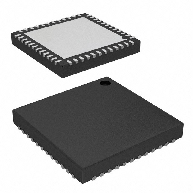
32-Pin Part Pinout
Figure 3. CY7C60445 32-Pin enCoRe V LV Device
P0[3]
P0[7]
Vdd P0[6] 28 27
P0[4] 26
32 31
30
P0[5]
29
P 0[1] P2[7] P2[5] P2[3] P2[1] P3[3] P3[1] P1[7]
1 2 3 4 5 6 7 8
25
P0[2]
Vss
24 23
P0[0] P2[6] P2[4] P2[2] P2[0] P3[2] P3[0] XRES
QFN
(Top View)
9 10
11
12
13 14
15 P1[4]
P1[5]
P1[1]
P1[3]
P1[0]
Vss
P1[2]
Table 1. 32-Pin Part Pinout (QFN) Pin No. 1 2 3 4 5 6 7 8 9 10 11 12 13 Type IOH IO IO IO IO IO IO IOHR IOHR IOHR IOHR Power IOHR Name P0[1] P2[7] P2[5] P2[3] P2[1] P3[3] P3[1] P1[7] P1[5] P1[3] P1[1](1, 2) Vss P1[0](1, 2) Digital IO Digital IO Digital IO, Crystal Out (Xout) Digital IO, Crystal In (Xin) Digital IO Digital IO Digital IO Digital IO, I2C SCL, SPI SS Digital IO, I2C SDA, SPI MISO Digital IO, SPI CLK Digital IO, ISSP CLK, I2C SCL, SPI MOSI Ground connection Digital IO, ISSP DATA, I2C SDA, SPI CLK Description
Note 1. During power up or reset event, device P1[0] and P1[1] may disturb the I2C bus. Use alternate pins if issues are encountered. 2. These are the in-system serial programming (ISSP) pins, that are not High Z at power on reset (POR).
Document Number: 001-12395 Rev. *F
P1[6]
16
22 21 20 19 18 17
Page 6 of 27
[+] Feedback
�PRELIMINARY
CY7C60445, CY7C6045x
Table 1. 32-Pin Part Pinout (QFN) (continued) Pin No. 14 15 16 17 18 19 20 21 22 23 24 25 26 27 28 29 30 31 32 CP Type IOHR IOHR IOHR Reset Input IO IO IO IO IO IO IOH IOH IOH IOH Power IOH IOH IOH Power Power Name P1[2] P1[4] P1[6] XRES P3[0] P3[2] P2[0] P2[2] P2[4] P2[6] P0[0] P0[2] P0[4] P0[6] Vdd P0[7] P0[5] P0[3] Vss Vss Digital IO Digital IO, optional external clock input (EXTCLK) Digital IO Active high external reset with internal pull down Digital IO Digital IO Digital IO Digital IO Digital IO Digital IO Digital IO Digital IO Digital IO Digital IO Supply voltage Digital IO Digital IO Digital IO Ground connection Center pad must be connected to ground Description
LEGEND I = Input, O = Output, OH = 5 mA High Output Drive, R = Regulated Output.
Document Number: 001-12395 Rev. *F
Page 7 of 27
[+] Feedback
�PRELIMINARY
CY7C60445, CY7C6045x
48-Pin Part Pinout
Figure 4. CY7C60455/CY7C60456 48-Pin enCoRe V LV Device
P0[4] 39
P0[2] 38
P0[3]
P0[5]
P0[7]
P0[1]
48
47
46
45
44
43
42 41
NC NC
40
P0[6]
37
NC P2[7] P2[5] P2[3] P2[1] P4[3] P4[1] P3[7] P3[5] P3[3] P3[1] P1[7]
1 2 3 4 5 6 7 8 9
P0[0] 36 35 34 33 32
Vdd
Vss
P2[6] P2[4] P2[2] P2[0] P4[2] P4[0] P3[6] P3[4] P3[2] P3[0] XRES P1[6]
QFN
(Top View)
31 30 29 28 27 26 25
10 11 12 13 14 15 16 17 18 19 20 21 22 P1[0] 23 24 P1[2]
P1[3]
P1[1]
P1[5]
Table 2. 48-Pin Part Pinout (QFN) Pin No. 1 2 3 4 5 6 7 8 9 10 11 12 13 14 15 Type NC IO IO IO IO IO IO IO IO IO IO IOHR IOHR NC NC NC P2[7] P2[5] P2[3] P2[1] P4[3] P4[1] P3[7] P3[5] P3[3] P3[1] P1[7] P1[5] NC NC Name No connection Digital I/O Digital I/O, Crystal Out (Xout) Digital I/O, Crystal In (Xin) Digital I/O Digital I/O Digital I/O Digital I/O Digital I/O Digital I/O Digital I/O Digital I/O, I2C SCL, SPI SS Digital I/O, I2C SDA, SPI MISO No connection No connection Description
Document Number: 001-12395 Rev. *F
P1[4]
NC
NC
Vss
NC
Vdd
NC
Page 8 of 27
[+] Feedback
�PRELIMINARY
CY7C60445, CY7C6045x
Table 2. 48-Pin Part Pinout (QFN) (continued) Pin No. 16 17 18 19 20 21 22 23 24 25 26 27 28 29 30 31 32 33 34 35 36 37 38 39 40 41 42 43 44 45 46 47 48 CP Type IOHR IOHR Power NC NC Power IOHR IOHR IOHR IOHR XRES IO IO IO IO IO IO IO IO IO IO IOH IOH IOH IOH Power NC NC IOH IOH IOH Power IOH Power Name P1[3] P1[1] Vss NC NC Vdd P1[0] P1[2] P1[4] P1[6] Ext Reset P3[0] P3[2] P3[4] P3[6] P4[0] P4[2] P2[0] P2[2] P2[4] P2[6] P0[0] P0[2] P0[4] P0[6] Vdd NC NC P0[7] P0[5] P0[3] Vss P0[1] Vss
(1, 2) (1, 2)
Description Digital I/O, SPI CLK Digital I/O, ISSP CLK, I2C SCL, SPI MOSI Supply ground No connection No connection Supply voltage Digital I/O, ISSP DATA, I2C SDA, SPI CLK Digital I/O Digital I/O, optional external clock input (EXTCLK) Digital I/O Active high external reset with internal pull down Digital I/O Digital I/O Digital I/O Digital I/O Digital I/O Digital I/O Digital I/O Digital I/O Digital I/O Digital I/O Digital I/O Digital I/O Digital I/O Digital I/O Supply voltage No connection No connection Digital I/O Digital I/O Digital I/O Supply ground Digital I/O Center pad must be connected to ground
LEGEND I = Input, O = Output, OH = 5 mA High Output Drive, R = Regulated Output
Document Number: 001-12395 Rev. *F
Page 9 of 27
[+] Feedback
�PRELIMINARY
CY7C60445, CY7C6045x
Register Reference
The section discusses the registers of the enCoRe V LV device. It lists all the registers in mapping tables, in address order.
Register Conventions
The register conventions specific to this section are listed in the following table. Table 3. Register Conventions Convention R W O L C # Description Read register or bits Write register or bits Only a read/write register or bits Logical register or bits Clearable register or bits Access is bit specific
Register Mapping Tables
The enCoRe V LV device has a total register address space of 512 bytes. The register space is also referred to as IO space and is broken into two parts: Bank 0 (user space) and Bank 1 (configuration space). The XIO bit in the Flag register (CPU_F) determines which bank the user is currently in. When the XIO bit is set, the user is said to be in the “extended” address space or the “configuration” registers.
Table 4. Register Map Bank 0 Table: User Space
Addr Addr Name Name (0,Hex) Access (0,Hex) Access PRT0DR 00 RW 40 PRT0IE 01 RW 41 02 42 03 43 PRT1DR 04 RW 44 PRT1IE 05 RW 45 06 46 07 47 PRT2DR 08 RW 48 PRT2IE 09 RW 49 0A 4A 0B 4B PRT3DR 0C RW 4C PRT3IE 0D RW 4D 0E 4E 0F 4F PRT4DR 10 RW 50 PRT4IE 11 RW 51 12 52 13 53 14 54 15 55 16 56 17 57 18 58 19 59 1A 5A 1B 5B 1C 5C 1D 5D 1E 5E 1F 5F 20 60 21 61 22 62 23 63 24 64 Gray fields are reserved and should not be accessed. # Access is bit specific. Name Addr Addr Name (0,Hex) Access (0,Hex) Access 80 C0 81 C1 82 C2 83 C3 84 C4 85 C5 86 C6 87 C7 88 I2C_XCFG C8 RW 89 I2C_XSTAT C9 R 8A I2C_ADDR CA RW 8B I2C_BP CB R 8C I2C_CP CC R 8D CPU_BP CD RW 8E CPU_CP CE R 8F I2C_BUF CF RW 90 CUR_PP D0 RW 91 STK_PP D1 RW 92 D2 93 IDX_PP D3 RW 94 MVR_PP D4 RW 95 MVW_PP D5 RW 96 I2C_CFG D6 RW 97 I2C_SCR D7 # 98 I2C_DR D8 RW 99 D9 9A INT_CLR0 DA RW 9B INT_CLR1 DB RW 9C INT_CLR2 DC RW 9D INT_CLR3 DD RW 9E INT_MSK2 DE RW 9F INT_MSK1 DF RW A0 INT_MSK0 E0 RW A1 INT_SW_EN E1 RW A2 INT_VC E2 RC A3 RES_WDT E3 W A4 INT_MSK3 E4 RW
Document Number: 001-12395 Rev. *F
Page 10 of 27
[+] Feedback
�PRELIMINARY
CY7C60445, CY7C6045x
Table 4. Register Map Bank 0 Table: User Space (continued)
Addr Addr Name Name (0,Hex) Access (0,Hex) Access 25 65 26 66 27 67 28 68 SPI_TXR 29 W 69 SPI_RXR 2A R 6A SPI_CR 2B # 6B 2C 6C 2D 6D 2E 6E 2F 6F 30 70 PT0_CFG 31 71 PT0_DATA1 32 72 PT0_DATA0 33 73 PT1_CFG 34 74 PT1_DATA1 35 75 PT1_DATA0 36 76 PT2_CFG 37 77 PT2_DATA1 38 78 PT2_DATA0 39 79 3A 7A 3B 7B 3C 7C 3D 7D 3E 7E 3F 7F Gray fields are reserved and should not be accessed. # Access is bit specific. Name Addr Name (0,Hex) Access A5 A6 A7 A8 A9 AA AB AC AD AE AF B0 RW B1 RW B2 RW B3 RW B4 RW B5 RW B6 RW B7 RW CPU_F B8 RW B9 BA BB BC BD BE CPU_SCR1 BF CPU_SCR0 Addr (0,Hex) Access E5 E6 E7 E8 E9 EA EB EC ED EE EF F0 F1 F2 F3 F4 F5 F6 F7 RL F8 F9 FA FB FC FD FE # FF #
Document Number: 001-12395 Rev. *F
Page 11 of 27
[+] Feedback
�PRELIMINARY
CY7C60445, CY7C6045x
Table 5. Register Map Bank 1 Table: Configuration Space
Addr Addr Addr Access Name Access Name (1,Hex) (1,Hex) (1,Hex) PRT0DM0 00 RW 40 80 PRT0DM1 01 RW 41 81 02 42 82 03 43 83 PRT1DM0 04 RW 44 84 PRT1DM1 05 RW 45 85 06 46 86 07 47 87 PRT2DM0 08 RW 48 88 PRT2DM1 09 RW 49 89 0A 4A 8A 0B 4B 8B PRT3DM0 0C RW 4C 8C PRT3DM1 0D RW 4D 8D 0E 4E 8E 0F 4F 8F PRT4DM0 10 RW 50 90 PRT4DM1 11 RW 51 91 12 52 92 13 53 93 14 54 94 15 55 95 16 56 96 17 57 97 18 58 98 19 59 99 1A 5A 9A 1B 5B 9B 1C 5C 9C 1D 5D 9D 1E 5E 9E 1F 5F 9F 20 60 A0 21 61 A1 22 62 A2 23 63 A3 24 64 A4 25 65 A5 26 66 A6 27 67 A7 28 68 A8 SPI_CFG 29 RW 69 A9 2A 6A AA 2B 6B AB 2C TMP_DR0 6C RW AC 2D TMP_DR1 6D RW AD 2E TMP_DR2 6E RW AE 2F TMP_DR3 6F RW AF 30 70 B0 31 71 B1 32 72 B2 33 73 B3 34 74 B4 35 75 B5 36 76 B6 37 77 B7 38 78 B8 39 79 B9 3A 7A BA Gray fields are reserved and should not be accessed. # Access is bit specific. Name Access Addr (1,Hex) C0 C1 C2 C3 C4 C5 C6 C7 C8 C9 CA CB CC CD CE CF D0 D1 D2 D3 D4 D5 D6 D7 D8 D9 DA DB IO_CFG DC OUT_P1 DD DE DF OSC_CR0 E0 ECO_CFG E1 OSC_CR2 E2 VLT_CR E3 VLT_CMP E4 E5 E6 E7 IMO_TR E8 ILO_TR E9 EA SLP_CFG EB SLP_CFG2 EC SLP_CFG3 ED EE EF F0 F1 F2 F3 F4 F5 F6 CPU_F F7 F8 F9 FA Name Access
RW RW
RW # RW RW R
W W RW RW RW
RL
Document Number: 001-12395 Rev. *F
Page 12 of 27
[+] Feedback
�PRELIMINARY
CY7C60445, CY7C6045x
Table 5. Register Map Bank 1 Table: Configuration Space
Addr Addr Addr Name Name (1,Hex) Access (1,Hex) Access (1,Hex) 3B 7B BB 3C 7C BC 3D 7D BD 3E 7E BE 3F 7F BF Gray fields are reserved and should not be accessed. # Access is bit specific. Name Access Name Addr (1,Hex) FB FC FD FE FF Access
Document Number: 001-12395 Rev. *F
Page 13 of 27
[+] Feedback
�PRELIMINARY
CY7C60445, CY7C6045x
Electrical Specifications
This section presents the DC and AC electrical specifications of the enCoRe V LV devices. For the most up to date electrical specifications, verify that you have the most recent data sheet available by visiting the company web site at http://www.cypress.com. Figure 5. Voltage versus CPU Frequency
3.6V
Figure 6. IMO Frequency Trim Options
3.6V
lid ng Va rati n pe gio Re O
Vdd Voltage
Vdd Voltage
SLIMO Mode = 01
SLIMO Mode = 00
SLIMO Mode = 10
1.71V
1.71V
750 kHz
3 MHz CPU Frequency
24 MHz
750 kHz
3 MHz
6 MHz 12 MHz 24 MHz
IMO Frequency
The following table lists the units of measure that are used in this chapter. Table 6. Units of Measure Symbol oC dB fF Hz KB Kbit kHz kΩ MHz MΩ μA μF μH μs μV μVrms Unit of Measure degree Celsius decibels femto farad hertz 1024 bytes 1024 bits kilohertz kilohm megahertz megaohm microampere microfarad microhenry microsecond microvolts microvolts root-mean-square Symbol μW mA ms mV nA ns nV W pA pF pp ppm ps sps s V Unit of Measure microwatts milli-ampere milli-second milli-volts nanoampere nanosecond nanovolts ohm picoampere picofarad peak-to-peak parts per million picosecond samples per second sigma: one standard deviation volts
Document Number: 001-12395 Rev. *F
Page 14 of 27
[+] Feedback
�PRELIMINARY
CY7C60445, CY7C6045x
Electrical Characteristics
Absolute Maximum Ratings
Storage Temperature (TSTG) (3) ............................................. ...................................................... -55oC to 125oC (Typical +25oC) Supply Voltage Relative to Vss (Vdd) .................................... ................................................................................. -0.5V to +4.0V DC Input Voltage (VIO)........................................................... ................................................................. Vss - 0.5V to Vdd + 0.5V DC Voltage Applied to Tri-state (VIOZ) ................................... ................................................................. Vss - 0.5V to Vdd + 0.5V Maximum Current into any Port Pin (IMIO)............................. ............................................................................. -25mA to +50mA Electro Static Discharge Voltage (ESD) (4) ............................ .............................................................................................. 2000V Latch-up Current (LU) (5) ....................................................... ............................................................................................. 200mA
Operating Conditions
Ambient Temperature (TA) ..................................................... .....................................................................................0oC to 70oC Operational Die Temperature (TJ)(6) ...................................... .....................................................................................0oC to 85oC
DC Electrical Characteristics
DC Chip Level Specifications
Table 7 lists guaranteed maximum and minimum specifications for the entire voltage and temperature ranges. Table 7. DC Chip Level Specifications Parameter Vdd IDD24 Description Supply Voltage Supply Current, IMO = 24 MHz Conditions See table titled DC POR and LVD Specifications on page 19. Conditions are Vdd = 3.0V, TA = 25oC, CPU = 24 MHz No I2C/SPI Conditions are Vdd = 3.0V, TA = 25oC, CPU = 12 MHz No I2C/SPI Conditions are Vdd = 3.0V, TA = 25oC, CPU = 6 MHz No I2C/SPI Vdd = 3.0V, TA = 25oC, IO regulator turned off Vdd = 3.0V, TA = 25oC, IO regulator turned off Min 1.71 – Typ – – Max 3.6 3.1 Units V mA
IDD12
Supply Current, IMO = 12 MHz
–
–
2.0
mA
IDD6
Supply Current, IMO = 6 MHz
–
–
1.5
mA
ISB0 ISB1
Deep Sleep Current Standby Current with POR, LVD and Sleep Timer
– –
0.1 –
– 1.5
μA μA
Notes 3. Higher storage temperatures reduce data retention time. Recommended storage temperature is +25°C ± 25°C. Extended duration storage temperatures above 85°C degrade reliability. 4. Human Body Model ESD. 5. Per JESD78 standard. 6. The temperature rise from ambient to junction is package specific. See Package Diagram on page 24 for Thermal Impedances. The user must limit the power consumption to comply with this requirement.
Document Number: 001-12395 Rev. *F
Page 15 of 27
[+] Feedback
�PRELIMINARY
CY7C60445, CY7C6045x
DC General Purpose IO Specifications
The following tables list guaranteed maximum and minimum specifications for the voltage and temperature ranges: 1.71V to 3.6V and 0°C ≤ TA ≤ 70°C. Typical parameters apply to 3.3V at 25°C. These are for design guidance only. Table 8. 3.0V to 3.6V DC GPIO Specifications Symbol RPU VOH1 VOH2 VOH3 Description Pull up Resistor High Output Voltage Port 2 or 3 Pins High Output Voltage Port 2 or 3 Pins High Output Voltage Port 0 or 1 Pins with LDO Regulator Disabled for Port 1 High Output Voltage Port 0 or 1 Pins with LDO Regulator Disabled for Port 1 High Output Voltage Port 1 Pins with LDO Regulator Enabled for 3V Out High Output Voltage Port 1 Pins with LDO Regulator Enabled for 3V Out IOH < 10 μA, maximum of 10 mA source current in all IOs IOH = 1 mA, maximum of 20 mA source current in all IOs IOH < 10 μA, maximum of 10 mA source current in all IOs IOH = 5 mA, maximum of 20 mA source current in all IOs IOH < 10 μA, Vdd > 3.1V, maximum of 4 IOs all sourcing 5 mA IOH = 5 mA, Vdd > 3.1V, maximum of 20 mA source current in all IOs Conditions Min 4 Vdd - 0.2 Vdd - 0.9 Vdd - 0.2 Typ 5.6 – – – Max 8 – – – Units kΩ V V V
VOH4
Vdd - 0.9
–
–
V
VOH5
2.85
3.00
3.15
V
VOH6
2.20
–
–
V
VOH7
High Output Voltage IOH < 10 μA, Vdd > 2.7V, maximum of Port 1 Pins with LDO Enabled for 2.5V 20 mA source current in all IOs Out High Output Voltage IOH = 2 mA, Vdd > 2.7V, maximum of Port 1 Pins with LDO Enabled for 2.5V 20 mA source current in all IOs Out IOH < 10 μA, Vdd > 2.7V, maximum of High Output Voltage Port 1 Pins with LDO Enabled for 1.8V 20 mA source current in all IOs Out High Output Voltage IOH = 1 mA, Vdd > 2.7V, maximum of Port 1 Pins with LDO Enabled for 1.8V 20 mA source current in all IOs Out Low Output Voltage IOL = 25 mA, Vdd > 3.3V, maximum of 60 mA sink current on even port pins (for example, P0[2] and P1[4]) and 60 mA sink current on odd port pins (for example, P0[3] and P1[5])
2.35
2.50
2.65
V
VOH8
1.90
–
–
V
VOH9
1.60
1.80
2.00
V
VOH10
1.20
–
–
V
VOL
–
–
0.75
V
VIL VIH VH IIL CIN COUT
Input Low Voltage Input High Voltage Input Hysteresis Voltage Input Leakage (Absolute Value) Capacitive Load on Pins as Input Capacitive Load on Pins as Output Gross tested to 1 µA. Package and pin dependent Temp = 25oC Package and pin dependent Temp = 25oC
– 2.00 – – 0.5 0.5
– – 80 1 1.7 1.7
0.80 – 5 5
V V mV nA pF pF
Document Number: 001-12395 Rev. *F
Page 16 of 27
[+] Feedback
�PRELIMINARY
CY7C60445, CY7C6045x
Table 9. 2.4V to 3.0V DC GPIO Specifications Symbol RPU VOH1 VOH2 VOH3 Description Pull up Resistor High Output Voltage Port 2 or 3 Pins High Output Voltage Port 2 or 3 Pins High Output Voltage Port 0 or 1 Pins with LDO Regulator Disabled for Port 1 High Output Voltage Port 0 or 1 Pins with LDO Regulator Disabled for Port 1 High Output Voltage Port 1 Pins with LDO Enabled for 1.8V Out High Output Voltage Port 1 Pins with LDO Enabled for 1.8V Out Low Output Voltage Conditions IOH < 10 μA, maximum of 10 mA source current in all IOs IOH = 0.2 mA, maximum of 10 mA source current in all IOs IOH < 10 μA, maximum of 10 mA source current in all IOs IOH = 2 mA, maximum of 10 mA source current in all IOs IOH < 10 μA, Vdd > 2.4V, maximum of 20 mA source current in all IOs. IOH = 1 mA, Vdd > 2.4V, maximum of 20 mA source current in all IOs IOL = 10 mA, maximum of 30 mA sink current on even port pins (for example, P0[2] and P1[4]) and 30 mA sink current on odd port pins (for example, P0[3] and P1[5]) Min 4 Vdd - 0.2 Vdd - 0.4 Vdd - 0.2 Typ 5.6 – – – Max 8 – – – Units kΩ V V V
VOH4
Vdd - 0.5
–
–
V
VOH5A
1.50
1.80
2.00
V
VOH6A
1.20
–
–
V
VOL
–
–
0.75
V
VIL VIH VH IIL CIN COUT
Input Low Voltage Input High Voltage Input Hysteresis Voltage Input Leakage (Absolute Value) Capacitive Load on Pins as Input Capacitive Load on Pins as Output
Gross tested to 1 µA. Package and pin dependent Temp = 25oC Package and pin dependent Temp = 25oC
– 2.0 – – 0.5 0.5
– – 80 1 1.7 1.7
0.72 – – 5 5
V V mV nA pF pF
Document Number: 001-12395 Rev. *F
Page 17 of 27
[+] Feedback
�PRELIMINARY
CY7C60445, CY7C6045x
Table 10. 1.71V to 2.4V DC GPIO Specifications Symbol RPU VOH1 VOH2 VOH3 Description Pull up Resistor High Output Voltage Port 2 or 3 Pins High Output Voltage Port 2 or 3 Pins High Output Voltage Port 0 or 1 Pins with LDO Regulator Disabled for Port 1 High Output Voltage Port 0 or 1 Pins with LDO Regulator Disabled for Port 1 Low Output Voltage IOH = 10 μA, maximum of 10 mA source current in all IOs IOH = 0.5 mA, maximum of 10 mA source current in all IOs IOH = 100 μA, maximum of 10 mA source current in all IOs IOH = 2 mA, maximum of 10 mA source current in all IOs IOL = 5 mA, maximum of 20 mA sink current on even port pins (for example, P0[2] and P1[4]) and 30 mA sink current on odd port pins (for example, P0[3] and P1[5]) Conditions Min 4 Vdd - 0.2 Vdd - 0.5 Vdd - 0.2 Typ 5.6 – – – Max 8 – – – Units kΩ V V V
VOH4
Vdd - 0.5
–
–
V
VOL
–
–
0.4
V
VIL VIH VH IIL CIN COUT
Input Low Voltage Input High Voltage Input Hysteresis Voltage Input Leakage (Absolute Value) Capacitive Load on Pins as Input Capacitive Load on Pins as Output Gross tested to 1 µA. Package and pin dependent. Temp = 25oC Package and pin dependent Temp = 25oC
– 0.65 x Vdd – – 0.5 0.5
– – 80 1
0.3 x Vdd – – 5 5
V V mV nA pF pF
Document Number: 001-12395 Rev. *F
Page 18 of 27
[+] Feedback
�PRELIMINARY
CY7C60445, CY7C6045x
DC POR and LVD Specifications
Table 11 lists guaranteed maximum and minimum specifications for the entire voltage and temperature ranges. Table 11. DC POR and LVD Specifications Symbol VPPOR0 VPPOR1 VPPOR2 VPPOR3 VLVD0 VLVD1 VLVD2 VLVD3 VLVD4 VLVD5 VLVD6 Description Vdd Value for PPOR Trip PORLEV[1:0] = 00b, HPOR = 0 PORLEV[1:0] = 00b, HPOR = 1 PORLEV[1:0] = 01b, HPOR = 1 PORLEV[1:0] = 10b, HPOR = 1 Vdd Value for LVD Trip VM[2:0] = 000b(8) VM[2:0] = 001b(9) VM[2:0] = 010b(10) VM[2:0] = 011b VM[2:0] = 100b VM[2:0] = 101b VM[2:0] = 110b(11)
(7)
Min 1.61
Typ 1.66 2.36 2.60 2.82 2.45 2.71 2.92 3.02 3.13 1.9 1.8
Max 1.71 2.40 2.65 2.95 2.51 2.78 2.99 3.09 3.20 – –
Units V V V V V V V V
2.40 2.64 2.85 2.95 3.06 – –
DC Programming Specifications
Table 12 lists guaranteed maximum and minimum specifications for the entire voltage and temperature ranges. Table 12. DC Programming Specifications Symbol VddIWRITE IDDP VILP VIHP IILP IIHP VOLV VOHV FlashENPB FlashDR Description Supply Voltage for Flash Write Operations Supply Current During Programming or Verify Input Low Voltage During Programming or Verify Input High Voltage During Programming or Verify Input Current when Applying Vilp to P1[0] or P1[1] During Programming or Verify(12) Input Current when Applying Vihp to P1[0] or P1[1] During Programming or Verify(13) Output Low Voltage During Programming or Verify Output High Voltage During Programming or Verify Flash Write Endurance(14) Flash Data Retention(15) Min 1.71 – – VIH – – – Vdd - 1.0 50,000 10 Typ – 5 – – – – – – – 20 Max – 25 VIL – 0.2 1.5 Vss + 0.75 Vdd – – Units V mA V V mA mA V V Cycles Years
Notes 7. Vdd must be greater than or equal to 1.71V during startup, reset from the XRES pin, or reset from watchdog. 8. Always greater than 50 mV above VPPOR1 for falling supply. 9. Always greater than 50 mV above VPPOR2 for falling supply. 10. Always greater than 50 mV above VPPOR3 for falling supply. 11. Always greater than 50 mV above VPPOR0 voltage for falling supply. 12. Driving internal pull down resistor. 13. Driving internal pull down resistor. 14. Erase/write cycles per block. 15. Following maximum Flash write cycles.
Document Number: 001-12395 Rev. *F
Page 19 of 27
[+] Feedback
�PRELIMINARY
CY7C60445, CY7C6045x
AC Electrical Characteristics
AC Chip Level Specifications
Table 13 lists guaranteed maximum and minimum specifications for the entire voltage and temperature ranges. Table 13. AC Chip Level Specifications Symbol FMAX FCPU F32K1 FIMO24 FIMO12 FIMO6 DCIMO TRAMP Description Maximum Operating Frequency(16) Maximum Processing Frequency(17) Internal Low Speed Oscillator Frequency Internal Main Oscillator Stability for 24 MHz ± 5%(18) Internal Main Oscillator Stability for 12 MHz(19) Internal Main Oscillator Stability for 6 MHz(20) Duty Cycle of IMO Supply Ramp Time Min 24 24 30.4 22.8 11.4 5.7 40 0 Typ – – 32 24 12 6.0 50 – Max – – 33.6 25.2 12.6 6.3 60 – Units MHz MHz kHz MHz MHz MHz % μs
Notes 16. Digital clocking functions. 17. CPU speed. 18. Trimmed using factory trim values. 19. Trimmed using factory trim values. 20. Trimmed using factory trim values.
Document Number: 001-12395 Rev. *F
Page 20 of 27
[+] Feedback
�PRELIMINARY
CY7C60445, CY7C6045x
AC General Purpose IO Specifications
Table 14 lists guaranteed maximum and minimum specifications for the entire voltage and temperature ranges. Table 14. AC GPIO Specifications Symbol FGPIO Description GPIO Operating Frequency Conditions Normal Strong Mode, Port 0, 1 Min 0 0 0 Normal Strong Mode, Port 2, 3 0 0 0 TRise023 Rise Time, Strong Mode, Cload = 50 pF Ports 2 or 3 Vdd = 3.0 to 3.6V, 10% – 90% Vdd = 2.4 to 3.0V, 10% – 90% TRise023L Rise Time, Strong Mode Low Supply, Cload = 50 pF Ports 2 or 3 TRise1 Rise Time, Strong Mode, Cload = 50 pF Ports 0 or 1 Vdd = 1.71 to 3.0V, 10% – 90% 15 15 15 Typ – – – – – – – – – Max 3 MHz for 1.71V


 工商网监
湘ICP备2023018690号
工商网监
湘ICP备2023018690号
