CY7C65100
CY7C65100 Four-port Universal Serial Bus Fixed-function Hub Controller
Cypress Semiconductor Corporation Document #: 38-08021 Rev. **
•
3901 North First Street
•
San Jose
•
CA 95134 • 408-943-2600 Revised June 6, 2002
�CY7C65100
TABLE OF CONTENTS 1.0 FEATURES ...................................................................................................................................... 3
2.0 FUNCTIONAL OVERVIEW .............................................................................................................. 3 3.0 PRODUCT SUMMARY .................................................................................................................... 4 3.1 Logic Block Diagram ...................................................................................................................... 4 3.2 Pin Configuration ............................................................................................................................ 4 3.3 Pin Assignments ............................................................................................................................. 5 4.0 CLOCKING ....................................................................................................................................... 5 5.0 USB OVERVIEW .............................................................................................................................. 5 5.1 USB SIE ........................................................................................................................................... 5 5.2 Hub Design ...................................................................................................................................... 6 5.3 Vendor ID and Product ID .............................................................................................................. 6 6.0 APPLICATION DIAGRAMS ............................................................................................................ 7 6.1 USB Standalone Hub Schematics ................................................................................................. 8 7.0 ABSOLUTE MAXIMUM RATINGS .................................................................................................. 9 8.0 ELECTRICAL CHARACTERISTICS ................................................................................................ 9 9.0 SWITCHING CHARACTERISTICS ............................................................................................... 10 10.0 ORDERING INFORMATION ........................................................................................................ 10 11.0 PACKAGE DIAGRAM .................................................................................................................. 11
LIST OF FIGURES
Figure 4-1. Clock Oscillator On-chip Circuit ....................................................................................... 5 Figure 6-1. USB Standalone Hub Application Diagram...................................................................... 7 Figure 9-1. Clock Timing ..................................................................................................................... 10 Figure 9-2. USB Data Signal Timing................................................................................................... 10 LIST OF TABLES Table 3-1. Pin Assignments ................................................................................................................ 5
Document #: 38-08021 Rev. **
Page 2 of 12
�CY7C65100
1.0 Features
• Fixed-function four-port USB hub devices with integrated hub repeater, hub controller, Serial Interface Engine (SIE), and USB transceivers • USB Specification Compliance — Conforms to USB Specification, Rev. 1.1 • • • • • • • • — Complies with the USB HUB Device Class Supports self-powered and bus-powered applications Individual downstream port power switching Individual downstream port overcurrent detection Integrated USB transceivers reduce EMI Internal 48-MHz phase-locked loop (PLL) reduces design cost by requiring only an external 6-MHz crystal Operating voltage from 4.0V–5.5V DC Operating temperature from 0°–70° Celsius Available in a space-saving 28-lead SOIC package
2.0
Functional Overview
The CY7C65100 series offers high-performance fixed-function Universal Serial Bus (USB) hub devices that comply with USB Specification, Rev. 1.1. Up to four downstream USB ports are available to expand the USB attachment points available in your PC system. These self-contained devices require no firmware development for your design, thereby reducing the design risk associated with some microcontroller solutions. These Application Specific Standard Products (ASSP) can improve time-tomarket in a number of USB designs, including standalone hubs, motherboard hubs, and monitor hubs. The CY7C65100 series supports self-powered or bus-powered applications. Power management for all downstream ports supports power-switching and overcurrent detection with individual port control. The four downstream ports support both full-speed (12-Mbps signaling rate) and low-speed (1.5-Mbps signaling rate) devices. The CY7C65100 sereis has a reduced frequency (6MHz) crystal oscillator for lower system cost as well as improved EMI performance. The four-port CY7C65100 series is available in a cost-effective and space-saving 28-lead SOIC package.
Document #: 38-08021 Rev. **
Page 3 of 12
�CY7C65100
3.0
3.1
Product Summary
Logic Block Diagram D+[0] D-[0]
USB 1.1 Xcvr PLL Upstream USB Port
USB Serial Interface Engine
USB Hub Controller
USB Hub Repeater
Downstream Port 1 USB 1.1 Xcvr Port Power Control
Downstream Port 2 USB 1.1 Xcvr Port Power Control
Downstream Port 3 USB 1.1 Xcvr Port Power Control
Downstream Port 4 USB 1.1 Xcvr Port Power Control
D+[1] D-[1] PWR[1] OC[1] D+[2] D-[2] PWR[2] OC[2] D+[3] D-[3] PWR[3] OC[3] D+[4] D-[4] PWR[4] OC[4] 3.2 Pin Configuration
CY7C65100 28-pin SOIC
XTALOUT XTALIN VREF GND D+[0] D–[0] D+[1] D–[1] D+[2] D–[2] OC[4] OC[2] PWR[4] PWR[2] 1 2 3 4 5 6 7 8 9 10 11 12 13 14 28 27 26 25 24 23 22 21 20 19 18 17 16 15 VCC PSTAT[3/4] PSTAT[1/2] PWR_SEL D–[3] D+[3] D–[4] D+[4] GND GND PWR[1] PWR[3] OC[1] OC[3]
Document #: 38-08021 Rev. **
Page 4 of 12
�CY7C65100
3.3 Pin Assignments
Table 3-1. Pin Assignments Name D+[0], D–[0] D+[1], D–[1] D+[2], D–[2] D+[3], D–[3] D+[4], D–[4] PWR[1]– PWR[4] OC[1]–OC[4] XTALIN XTALOUT VCC GND VREF PWR_SEL PSTAT[1/2], PSTAT[3/4] I/O I/O I/O I/O I/O I/O OUT IN IN OUT PWR GND IN IN OUT Pin 5,6 7,8 9,10 23,24 21,22 18,14,17,13 16,12,15,11 2 1 28 4,19,20 3 25 26,27 Description Upstream port, USB differential data Downstream port 1, USB differential data Downstream port 2, USB differential data Downstream port 3, USB differential data Downstream port 4, USB differential data Downstream port power enable output Downstream port power over-current detection signals 6-MHz crystal or external clock input 6-MHz crystal out Voltage supply Ground Input for external 3.3V supply voltage for the upstream and downstream differential data output buffers and the D+ pull-up Bus or self-power function select input Downstream port LED status enable
4.0
Clocking
XTALOUT (pin 1)
XTALIN (pin 2) 30 pF
to internal PLL 30 pF
Figure 4-1. Clock Oscillator On-chip Circuit XTALIN and XTALOUT are the clock pins to the CY7C65100 series. The user can connect either an external oscillator or a crystal to these pins. A 6-MHz fundamental crystal can be connected to these pins to provide a reference frequency for the internal PLL. When using an external crystal, keep PCB traces between the chip leads and crystal as short as possible (less than 2 cm). A ceramic resonator is not an adequate clock source to meet the timing specifications of a high-speed USB function and therefore cannot be used with these parts. An external 6-MHz clock can be applied to the XTALIN pin if the XTALOUT pin is left open. Please note that grounding the XTALOUT pin when driving XTALIN with an oscillator will not work as the internal clock is effectively shorted to ground.
5.0
USB Overview
The USB hardware includes a USB Hub repeater with one upstream port and up to four downstream ports. An external series resistor of Rext = 20Ω (± 5%) must be placed in series with all upstream and downstream USB I/O in order to meet the USB driver impedance requirements as defined by the USB specification (see Figure 6-1).
5.1
USB SIE
The SIE allows the CY7C65100 series to communicate with the USB host through the USB repeater portion of the hub. The SIE handles the following USB bus activity independently of the hub microcontroller: • Bit stuffing/unstuffing • Checksum generation/checking Document #: 38-08021 Rev. ** Page 5 of 12
�CY7C65100
• ACK/NAK/STALL • TOKEN type identification • Address checking. The following protocol handling is done at a higher level by the Hub Control Block: • Coordinate enumeration by responding to SETUP packets • Fill and empty the FIFOs • Suspend/Resume coordination • Verify and select DATA toggle values • Port power control and over-current detection.
5.2
Hub Design
The power switching and over-current detection of downstream ports is managed by control pins connected to an external power switch device (see Figure 6-1). The active-LOW PWR[n] output pins of the CY7C65100 series are connected to the respective external power switch’s port power enable signals. (Note that each port power output pin of the external power switch must be bypassed with an electrolytic or tantalum capacitor as required by the USB specification. These capacitors supply the inrush currents which occur during downstream device hot-attach events.) The active-LOW OC[n] pins of the CY7C65100 series are connected to the respective external power switch’s port over-current indication (output) signals. Upon detecting an over-current condition, the hub device reports the over-current condition to the host and disables (sets to logic HIGH) the respective PWR[n] signal connected to the external power device.
5.3
Vendor ID and Product ID
The CY7C65100 Series will enumerate with the default Vendor ID and Product ID as follows. Bus-powered Vendor ID Product ID 0x04b4 0x5204 Self-powered 0x04b4 0x5203
Pin 25 (PWR_SEL) is a strapping option that selects the device’s power configuration report (PWR_SEL = GND for self-powered, PWR_SEL = Vcc for bus-powered). For high-volume business, Cypress has the capability to factory-program a Custom Vendor ID and Product ID. Please contact your local Cypress sales office for more information.
Document #: 38-08021 Rev. **
Page 6 of 12
�CY7C65100
6.0 Application Diagrams
+3.3V +5.0V
1.5K
(TO HOST)
D+ D– 20 20
VCC
D+[0] D–[0]
+3.3V
VREF
XTALIN XTALOUT
+5.0V
IN
+5.0V
100K
PWR1
VCC D+ D-
PWR1
OUTA
ENA FLGA
PWR[1] OC[1]
+5.0V
100K
D+[1] D–[1]
20 20 15K 15K
Port 1
PWR2
OUTB ENB FLGB
PWR2
VCC D+ D-
PWR[2] OC[2]
D+[2] D–[2]
20 20
15K
15K
Port 2
+5.0V
Power Switch
PWR3
OUTC ENC FLGC
CY7C65100 Series
PWR3
VCC D+ D-
100K
PWR[3] OC[3]
+5.0V
100K
D+[3] D–[3]
20 20
15K
15K
Port 3
PWR4
OUTD END FLGD
PWR4
VCC D+ D-
PWR[4] OC[4]
D+[4] D–[4]
20 20
15K
15K
Port 4
PWR1 PWR2 PWR3 PWR4
1K 1K 1K 1K
PSTAT[1/2] PWR_SEL* PSTAT[3/4] * PWR_SEL = VCC for Bus-powered Applications PWR_SEL = GND for Self-powered Applications
Figure 6-1. USB Standalone Hub Application Diagram
Document #: 38-08021 Rev. **
Page 7 of 12
�CY7C65100
6.1 USB Standalone Hub Schematics
Document #: 38-08021 Rev. **
Page 8 of 12
�CY7C65100
7.0 Absolute Maximum Ratings
Storage Temperature ................................. –65°C to +150°C Ambient Temperature with Power Applied ...... –0°C to +70°C Supply voltage on VCC relative to VSS ........... –0.5V to +7.0V DC Input Voltage................................. –0.5V to +VCC + 0.5V Power Dissipation .....................................................500 mW Static Discharge Voltage ..........................................> 2000V Latch-up Current ................................................... > 200 mA Max Output Sink Current into PWR[n] Pins (Vout = 2.0V) ............................................................... 60 mA
8.0
General Vref ICC IREF ISB1 IIL
Electrical Characteristics FOSC = 6 MHz; Operating Temperature = 0° to 70°C, VCC = 4.0V to 5.5V
Description Reference Voltage VCC Operating Current Vref Operating Current Standby Current Input Leakage Current Differential Input Sensitivity Differential Input Common Mode Range Single Ended Receiver Threshold Transceiver Capacitance High-Z State Data Line Leakage USB Power Setting Pull-up Resistor External USB Pull-down Resistor External USB Series Resistor VCC Ramp Rate Downstream data lines In series with each USB pin Linear ramp: VCC=0 to Operating Voltage[1] RL of 15 kΩ± 5% to Gnd RL of 1.5 kΩ± 5% to 3.6V 1.3 Including Rext 28 0V < Vin < 3.3V –10 1.425 14.25 19 0 any pin |(D+)–(D–)| 0.2 0.8 0.8 2.5 2.0 20 10 1.575 15.75 21 100 No USB Traffic 3.3V ± 5% Conditions Min. 3.15 Max. 3.45 50 10 50 1 Unit V mA mA µA µA V V V pF µA KW KW W ms
Parameter
USB Interface Vdi Vcm Vse Cin Ilo RD+ Rext1 Rext2 tvccs
Power-On Reset
USB Upstream/Downstream Port Voh Vol Vcrs Zo OC[n] Pins VIL VIH IPWR[n] Input LOW Threshold Voltage Input HIGH Threshold Voltage PWR[n] Sink Current (typical 7 mA) Vout = 2.0V DC 2.0 3.5 10.6 0.8 V V mA Static Output HIGH Static Output LOW Crossover Voltage USB Driver Output Impedance 2.8 3.6 0.3 2.0 44 V V V W
PWREN[n] Pins
Note: 1. Power-on Reset will occur whenever the voltage on VCC is below approximately 2.5V.
Document #: 38-08021 Rev. **
Page 9 of 12
�CY7C65100
Parameter Clock Source fOSC tcyc tCH tCL tr tf trfm tdrate tr tf trfm tdrate Clock Rate Clock Period Clock HIGH Time Clock LOW Time Transition Rise Time Transition Fall Time Rise/Fall Time Matching; (tr/tf) Full-speed Data Rate Transition Rise Time Transition Fall Time Rise/Fall Time Matching; (tr/tf) Low-speed Data Rate 5.985 166.25 0.45 tCYC 0.45 tCYC 4 4 90 11.97 75 75 80 1.4775 20 20 110 12.03 300 300 120 1.5225 6.015 167.08 MHz nsec ns ns ns ns % Mb/s ns ns % Mb/s Description Min. Max. Unit
USB Full-speed Signaling
USB Low-speed Signaling
9.0
Switching Characteristics
tCYC tCH
CLOCK
tCL Figure 9-1. Clock Timing tR 90%
D− 10% 90% 10%
D+
tF
Figure 9-2. USB Data Signal Timing
10.0
Ordering Information
Package Name S21 Description 28-pin SOIC Operating Range Commercial
Ordering Code CY7C65100-SC
Document #: 38-08021 Rev. **
Page 10 of 12
�CY7C65100
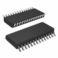
11.0 Package Diagram
28-lead (300-mil) Molded SOIC S21
51-85026-A
All product and company names mentioned in this document are the trademarks of their respective holders.
Document #: 38-08021 Rev. **
Page 11 of 12
© Cypress Semiconductor Corporation, 2002. The information contained herein is subject to change without notice. Cypress Semiconductor Corporation assumes no responsibility for the use of any circuitry other than circuitry embodied in a Cypress Semiconductor product. Nor does it convey or imply any license under patent or other rights. Cypress Semiconductor does not authorize its products for use as critical components in life-support systems where a malfunction or failure may reasonably be expected to result in significant injury to the user. The inclusion of Cypress Semiconductor products in life-support systems application implies that the manufacturer assumes all risk of such use and in doing so indemnifies Cypress Semiconductor against all charges.
�CY7C65100
Document Title: CY7C65100 Four-port Universal Serial Bus Fixed-function Hub Controller Document Number: 38-08021 REV. ** ECN NO. 113849 Issue Date 06/25/02 Orig. of Change BON New Data Sheet Description of Change
Document #: 38-08021 Rev. **
Page 12 of 12
�
很抱歉,暂时无法提供与“CY7C65100-SC”相匹配的价格&库存,您可以联系我们找货
免费人工找货