CY7C68000
TX2™ USB 2.0 UTMI Transceiver
1.0
EZ-USB TX2™ Features
The Cypress EZ-USB TX2™ is a Universal Serial Bus (USB)
specification revision 2.0 transceiver, serial/deserializer, to a
parallel interface of either 16 bits at 30 MHz or eight bits at 60
MHz. The TX2 provides a high-speed physical layer interface
that operates at the maximum allowable USB 2.0 bandwidth.
This allows the system designer to keep the complex highspeed analog USB components external to the digital ASIC
which decreases development time and associated risk. A
standard interface is provided that is USB 2.0-certified and is
compliant with Transceiver Macrocell Interface (UTMI) specification version 1.05 dated 3/29/01.
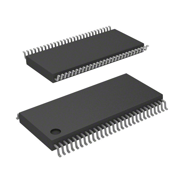
Two packages are defined for the family: 56-pin SSOP and 56pin QFN.
The function block diagram is shown in Figure 1-1. The
features of the EX-USB TX2 are:
• UTMI-compliant/USB-2.0-certified for device operation
• Operates in both USB 2.0 high speed (HS), 480
Mbits/second, and full speed (FS), 12 Mbits/second
• Serial-to-parallel and parallel-to-serial conversions
• 8-bit unidirectional, 8-bit bidirectional, or 16-bit
bidirectional external data interface
• Synchronous field and EOP detection on receive
packets
• Synchronous field and EOP generation on transmit
packets
• Data and clock recovery from the USB serial stream
• Bit stuffing/unstuffing; bit stuff error detection
• Staging register to manage data rate variation due to
bit stuffing/unstuffing
• 16-bit 30-MHz, and 8-bit 60-MHz parallel interface
• Ability to switch between FS and HS terminations and
signaling
• Supports detection of USB reset, suspend, and resume
• Supports HS identification and detection as defined by
the USB 2.0 Specification
• Supports transmission of resume signaling
• 3.3 V operation
• Two package options—56-pin QFN, and 56-pin SSOP
• All required terminations, including 1.5K-ohm pull up
on DPLUS, are internal to the chip
• Supports USB 2.0 test modes
CY7C68000
CY7C68000
XTALIN/
OUT
OSC
20X
PLL
PLL_480
UTMI CLK
Full-Speed Rx
High-Speed Rx
USB
USB
2.0
XCVR
Traffic
Sync
Fast
Digital
Rx
Elasticity
Buffer
Fast
Digital
Tx
High-Speed Tx
Full-Speed Tx
Digital
Rx
UTMI CLK
UTMI Rx Ctl
UTMI Rx Data 8/16
BIDI Option
Also
Digital
Tx
UTMI Tx
Rx Data 8/16
UTMI Tx Ctl
Figure 1-1. Block Diagram
Cypress Semiconductor Corporation
Document #: 38-08016 Rev. *H
•
198 Champion Court
•
San Jose, CA 95134-1709
•
408-943-2600
Revised May 2, 2006
[+] Feedback
�CY7C68000
2.0
•
•
•
•
•
•
•
•
•
•
Applications
DSL modems
ATA interface
Memory card readers
Legacy conversion devices
Cameras
Scanners
Home PNA
Wireless LAN
MP3 players
Networking
3.0
3.1
Functional Overview
3.6
TX2 does not support the low-speed (LS) signaling rate of 1.5
Mbps.
The FS vs. HS is done through the use of both XcvrSelect and
the TermSelect input signals. The TermSelect signal enables
the 1.5 K ohm pull up on to the DPLUS pin. When TermSelect
is driven LOW, a SE0 is asserted on the USB providing the HS
termination and generating the HS Idle state on the bus. The
XcvrSelect signal is the control which selects either the FS
transceivers or the HS transceivers. To select the HS transceivers, set this pin to ‘0’. To select the FS transceivers, set
this pin to ‘1’.
Transceiver Clock Frequency
3.7
An on-chip phase-locked loop (PLL) multiplies the 24-MHz
oscillator up to 30/60 MHz, as required by the transceiver
parallel data bus. The default UTMI interface clock (CLK)
frequency is determined by the DataBus16_8 pin.
Buses
The two packages allow for 8/16-bit bidirectional data bus for
data transfers to a controlling unit.
3.4
Reset Pin
An input pin (Reset) resets the chip. This pin has hysteresis
and is active HIGH according to the UTMI specification. The
internal PLL stabilizes approximately 200 μs after VCC has
reached 3.3V.
3.5
Line State
The Line State output pins LineState[1:0] are driven by combinational logic and may be toggling between the J and the K
states. They are synchronized to the CLK signal for a valid
Document #: 38-08016 Rev. *H
Operational Modes
The operational modes are controlled by the OpMode signals.
The OpMode signals are capable of inhibiting normal
operation of the transceiver and evoking special test modes.
These modes take effect immediately and take precedence
over any pending data operations. The transmission data rate
when in OpMode depends on the state of the XcvrSelect
input.
OpMode[1:0]
Mode
00
0
Normal operation
01
1
Non-driving
10
2
Disable Bit Stuffing and
NRZI encoding
11
3
Reserved
TX2 has an on-chip oscillator circuit that uses an external 24MHz (±100-ppm) crystal with the following characteristics:
• Parallel resonant
• Fundamental mode
• 500-μW drive level
• 27–33 pF (5% tolerance) load capacitors
3.3
Full-speed vs. High-speed Select
USB Signaling Speed
TX2 operates at two of the rates defined in the USB Specification 2.0, dated April 27, 2000:
• Full speed, with a signaling bit rate of 12 Mbps
• High speed, with a signaling bit rate of 480 Mbps
3.2
signal. On the CLK edge the state of these lines reflect the
state of the USB data lines. Upon the clock edge the 0-bit of
the LineState pins is the state of the DPLUS line and the one
bit of LineState is the DMINUS line. When synchronized, the
set up and hold timing of the LineState is identical to the
parallel data bus.
Description
Mode 0 allows the transceiver to operate with normal USB
data decoding and encoding.
Mode 1 allows the transceiver logic to support a soft
disconnect feature which three-states both the HS and FS
transmitters, and removes any termination from the USB,
making it appear to an upstream port that the device has been
disconnected from the bus.
Mode 2 disables Bit Stuff and NRZI encoding logic so 1s
loaded from the data bus becomes Js on the DPLUS/DMINUS
lines and 0s become Ks.
4.0
DPLUS/DMINUS Impedance Termination
The CY7C68000 does not require external resistors for USB
data line impedance termination or an external pull up resistor
on the DPLUS line. These resistors are incorporated into the
part. They are factory trimmed to meet the requirements of
USB 2.0. Incorporating these resistors also reduces the pin
count on the part.
Page 2 of 14
[+] Feedback
�CY7C68000
5.0
Pin Assignments
The following pages illustrate the individual pin diagrams that are available in the 56-pin QFN and 56-pin SSOP packages.
The packages offered use either an 8-bit (60-MHz) or 16-bit (30-MHz) bus interface.
56-pin QFN
ValidH
VCC
TXValid
GND
Uni_bidi
DataBus16_8
CLK
D0
D1
Reserved
D2
VCC
D3
D4
56
55
54
53
52
51
50
49
48
47
46
45
44
43
TXReady
1
42
GND
Suspend
2
41
D5
Reset
3
40
Reserved
AVCC
4
39
D6
XTALOUT
5
38
D7
XTALIN
6
37
D8
36
D9
CY7C68000
AGND
7
AVCC
8
35
Reserved
DPLUS
9
34
D10
DMINUS 10
33
D11
11
32
VCC
XcvrSelect 12
31
D12
TermSelect 13
30
GND
OpMode0 14
29
D13
AGND
56-pin QFN
15
16
17
18
19
20
21
22
23
24
25
26
27
28
OpMode1
GND
VCC
LineState0
LineState1
GND
RXValid
RXActive
RXError
Reserved
Reserved
D15
D14
VCC
Figure 5-1. CY7C68000 56-pin QFN Pin Assignment
Document #: 38-08016 Rev. *H
Page 3 of 14
[+] Feedback
�CY7C68000
56-pin SSOP
1
CLK
D0
56
2
DataBus16_8
D1
55
3
Uni_Bidi
Reserved
54
4
GND
D2
53
5
TXValid
VCC
52
6
VCC
D3
51
7
ValidH
D4
50
8
TXReady
GND
49
9
Suspend
D5
48
10
Reset
Reserved
47
11
AVCC
D6
46
12
XTALOUT
D7
45
13
XTALIN
D8
44
14
AGND
D9
43
15
AVCC
Reserved
42
16
DPLUS
D10
41
17
DMINUS
D11
40
18
AGND
VCC
39
19
XcvrSelect
D12
38
20
TermSelect
GND
37
21
OpMode0
D13
36
22
OpMode1
VCC
35
23
GND
D14
34
24
VCC
D15
33
25
LineState0
Reserved
32
26
LineState1
Reserved
31
27
GND
RXError
30
28
RXValid
RXActive
29
Figure 5-2. CY7C68000 56-pin SSOP Pin Assignment
5.1
CY7C68000 Pin Descriptions
Table 5-1. Pin Descriptions [1]
SSOP QFN
Type
Default
Description
11
4
AVCC
Name
Power
N/A
Analog VCC. This signal provides power to the analog section of the chip.
15
8
AVCC
Power
N/A
Analog VCC. This signal provides power to the analog section of the chip.
14
7
AGND
Power
N/A
Analog Ground. Connect to ground with as short a path as possible.
18
11
AGND
Power
N/A
Analog Ground. Connect to ground with as short a path as possible.
16
9
DPLUS
I/O/Z
Z
USB DPLUS Signal. Connect to the USB DPLUS signal.
17
10
DMINUS
I/O/Z
Z
USB DMINUS Signal. Connect to the USB DMINUS signal.
Note:
1. Unused inputs should not be left floating. Tie either HIGH or LOW as appropriate. Outputs that are three-statable should only be pulled up or down to ensure
signals at power-up and in standby.
Document #: 38-08016 Rev. *H
Page 4 of 14
[+] Feedback
�CY7C68000
Table 5-1. Pin Descriptions (continued)[1]
SSOP QFN
Name
Type
Default
Description
56
49
D0
I/O
55
48
D1
I/O
53
46
D2
I/O
51
44
D3
I/O
50
43
D4
I/O
48
41
D5
I/O
46
39
D6
I/O
45
38
D7
I/O
44
37
D8
I/O
43
36
D9
I/O
41
34
D10
I/O
40
33
D11
I/O
38
31
D12
I/O
36
29
D13
I/O
34
27
D14
I/O
33
26
D15
I/O
1
50
CLK
Output
10
3
Reset
Input
N/A
Active HIGH Reset. Resets the entire chip. This pin can be tied to VCC
through a 0.1 μF capacitor and to GND through a 100 K resistor for a 10
msec RC time constant.
19
12
XcvrSelect
Input
N/A
Transceiver Select. This signal selects between the Full Speed (FS) and
the High Speed (HS) transceivers:
0: HS transceiver enabled
1: FS transceiver enabled
20
13
TermSelect
Input
N/A
Termination Select. This signal selects between the between the Full
Speed (FS) and the High Speed (HS) terminations:
0: HS termination
1: FS termination
9
2
Suspend
Input
N/A
Suspend. Places the CY7C68000 in a mode that draws minimal power from
supplies. Shuts down all blocks not necessary for Suspend/Resume operations. While suspended, TermSelect must always be in FS mode to ensure
that the 1.5 K ohm pull-up on DPLUS remains powered.
0: CY7C68000 circuitry drawing suspend current
1: CY7C68000 circuitry drawing normal current
26
19
LineState1
Output
Line State. These signals reflect the current state of the single-ended
receivers. They are combinatorial until a “usable” CLK is available then they
are synchronized to CLK. They directly reflect the current state of the
DPLUS (LineState0) and DMINUS (LineState1).
D– D+ Description
0 0 0: SE0
0 1 1: ‘J’ State
1 0 2: ‘K’ State
1 1 3: SE1
25
18
LineState0
Output
Line State. These signals reflect the current state of the single-ended
receivers. They are combinatorial until a ‘usable’ CLK is available then they
are synchronized to CLK. They directly reflect the current state of the
DPLUS (LineState0) and DMINUS (LineState1).
D– D+ Description
00–0: SE0
01–1: ‘J’ State
10–2: ‘K’ State
11–3: SE1.
Document #: 38-08016 Rev. *H
Bidirectional Data Bus. This bidirectional bus is used as the entire data
bus in the 8-bit bidirectional mode or the least significant eight bits in the 16bit mode or under the 8-bit unidirectional mode these bits are used as inputs
for data, selected by the RxValid signal.
Bidirectional Data Bus. This bidirectional bus is used as the upper eight
bits of the data bus when in the 16-bit mode, and not used when in the 8-bit
bidirectional mode. Under the 8-bit unidirectional mode these bits are used
as outputs for data, selected by the TxValid signal.
Clock. This output is used for clocking the receive and transmit parallel data
on the D[15:0] bus.
Page 5 of 14
[+] Feedback
�CY7C68000
Table 5-1. Pin Descriptions (continued)[1]
SSOP QFN
Name
Type
Default
Description
22
15
OpMode1
Input
Operational Mode. These signals select among various operational
modes:
10 Description
00–0: Normal Operation
01–1: Non-driving
10–2: Disable Bit Stuffing and NRZI encoding
11–3: Reserved.
21
14
OpMode0
Input
Operational Mode. These signals select among various operational
modes:
10 Description
00–0: Normal Operation
01–1: Non-driving
10–2: Disable Bit Stuffing and NRZI encoding
11–3: Reserved.
5
54
TXValid
Input
Transmit Valid. Indicates that the data bus is valid. The assertion of Transmit Valid initiates SYNC on the USB. The negation of Transmit Valid initiates
EOP on the USB. The start of SYNC must be initiated on the USB no less
than one or no more that two CLKs after the assertion of TXValid.
In HS (XcvrSelect = 0) mode, the SYNC pattern must be asserted on the
USB between 8- and 16-bit times after the assertion of TXValid is detected
by the Transmit State Machine.
In FS (Xcvr = 1), the SYNC pattern must be asserted on the USB no less
than one or more than two CLKs after the assertion of TXValid is detected
by the Transmit State Machine.
8
1
TXReady
Output
Transmit Data Ready. If TXValid is asserted, the SIE must always have
data available for clocking in to the TX Holding Register on the rising edge
of CLK. If TXValid is TRUE and TXReady is asserted at the rising edge of
CLK, the CY7C68000 will load the data on the data bus into the TX Holding
Register on the next rising edge of CLK. At that time, the SIE should immediately present the data for the next transfer on the data bus.
28
21
RXValid
Output
Receive Data Valid. Indicates that the DataOut bus has valid data. The
Receive Data Holding Register is full and ready to be unloaded. The SIE is
expected to latch the DataOut bus on the clock edge.
29
22
RXActive
Output
Receive Active. Indicates that the receive state machine has detected
SYNC and is active.
RXActive is negated after a bit stuff error or an EOP is detected.
30
23
RXError
Output
Receive Error.
0 Indicates no error.
1 Indicates that a receive error has been detected.
7
56
ValidH
2
51
DataBus16_8
Document #: 38-08016 Rev. *H
I/O
ValidH. This signal indicates that the high-order eight bits of a 16-bit data
word presented on the Data bus are valid. When DataBus16_8 = 1 and
TXValid = 0, ValidH is an output, indicating that the high-order receive data
byte on the Data bus is valid. When DataBus16_8 = 1 and TXValid = 1,
ValidH is an input and indicates that the high-order transmit data byte,
presented on the Data bus by the transceiver, is valid. When DataBus16_8
= 0, ValidH is undefined. The status of the receive low-order data byte is
determined by RXValid and are present on D0–D7.
Input
Data Bus 16_8. Selects between 8- and 16-bit data transfers.
1–16-bit data path operation enabled. CLK = 30 MHz.
0–8-bit data path operation enabled. When Uni_Bidi = 0, D[8:15] are undefined. When Uni_Bidi =1, D[0:7] are valid on RxValid and D[8:15] are valid
on TxValid. CLK = 60 MHz
Note: DataBus16_8 is static after Power-on Reset (POR) and is only sampled at the end of Reset.
Page 6 of 14
[+] Feedback
�CY7C68000
Table 5-1. Pin Descriptions (continued)[1]
SSOP QFN
Name
Type
Default
Description
Input
N/A
Crystal Input. Connect this signal to a 24-MHz parallel-resonant, fundamental mode crystal and 20-pF capacitor to GND.
It is also correct to drive XTALIN with an external 24-MHz square wave
derived from another clock source.
Output
N/A
Crystal Output. Connect this signal to a 24-MHz parallel-resonant, fundamental mode crystal and 30-pF (nominal) capacitor to GND. If an external
clock is used to drive XTALIN, leave this pin open.
13
6
XTALIN
12
5
XTALOUT
3
52
Uni_Bidi
6
55
VCC
Power
24
17
VCC
Power
N/A
VCC. Connect to 3.3V power source.
35
28
VCC
Power
N/A
VCC. Connect to 3.3V power source.
39
32
VCC
Power
N/A
VCC. Connect to 3.3V power source.
52
45
VCC
Power
N/A
VCC. Connect to 3.3V power source.
4
53
GND
Ground
N/A
Ground.
23
16
GND
Ground
N/A
Ground.
27
20
GND
Ground
N/A
Ground.
37
30
GND
Ground
N/A
Ground.
49
42
GND
Ground
N/A
Ground.
31
24
Reserved
INPUT
Connect pin to Ground.
54
47
Reserved
INPUT
Connect pin to Ground.
47
40
Reserved
INPUT
Connect pin to Ground.
42
35
Reserved
INPUT
Connect pin to Ground.
32
25
Reserved
INPUT
Connect pin to Ground.
Document #: 38-08016 Rev. *H
Input
Driving this pin HIGH enables the unidirectional mode when the 8-bit
interface is selected. Uni_Bidi is static after power on reset (POR).
VCC. Connect to 3.3V power source.
Page 7 of 14
[+] Feedback
�CY7C68000
6.0
Absolute Maximum Ratings
7.0
Operating Conditions
Storage Temperature .................................–65°C to +150°C
TA (Ambient Temperature Under Bias) ............. 0°C to +70°C
Ambient Temperature with Power Supplied ...... 0°C to +70°C
Supply Voltage................................................+3.0V to +3.6V
Supply Voltage to Ground Potential ............... –0.5V to +4.0V
Ground Voltage.................................................................. 0V
DC Input Voltage to Any Input Pin .............................. 5.25 V
FOSC (Oscillator or Crystal Frequency).... 24 MHz ± 100 ppm
DC Voltage Applied to Outputs
in High-Z State .......................................–0.5V to VCC + 0.5V
................................................................... Parallel Resonant
Power Dissipation .....................................................630 mW
Static Discharge Voltage ...........................................> 2000V
Max Output Current, per IO pin..................................... 4 mA
Max Output Current, all 21–IO pins ............................84 mA
8.0
DC Characteristics
Table 8-1. DC Characteristics
Parameter
Description
VCC
Supply Voltage
VIH
Input High Voltage
VIL
Input Low Voltage
II
Input Leakage Current
Conditions
Min.
Typ.
3.0
3.3
2
–0.5
0< VIN < VCC
VOH
Output Voltage High
IOUT = 4 mA
VOL
Output Low Voltage
IOUT = –4 mA
Max.
Unit
3.6
V
5.25
V
0.8
V
±10
μA
0.4
V
2.4
V
IOH
Output Current High
4
mA
IOL
Output Current Low
4
mA
CIN
Input Pin Capacitance
Except DPLUS/DMINUS/CLK
10
pF
DPLUS/DMINUS/CLK
15
pF
CLOAD
Maximum Output Capacitance
Output pins
ISUSP
Suspend Current
Connected[2]
235
Disconnected[2]
15
ICC
Supply Current HS Mode
Normal operation OPMOD[1:0] = 00
ICC
Supply Current FS Mode
Normal operation OPMOD[1:0] = 00
tRESET
Minimum Reset time
8.1
1.9
30
pF
293
μA
55
μA
175
mA
90
mA
ms
USB 2.0 Transceiver
USB 2.0 compliant in FS and HS modes.
Note:
2. Connected to the USB includes 1.5k-ohm internal pull-up. Disconnected has the 1.5k-ohm internal pull-up excluded.
Document #: 38-08016 Rev. *H
Page 8 of 14
[+] Feedback
�CY7C68000
9.0
9.1
AC Electrical Characteristics
USB 2.0 Transceiver
USB 2.0 certified in FS and HS.
9.2
Timing Diagram
9.2.1
HS/FS Interface Timing–60 MHz
CLK
TCH_MIN
TCSU_MIN
Control_In
TDH_MIN
TDSU_MIN
DataIn
TCCO
Control_Out
TCDO
DataOut
Figure 9-1. 60-MHz Interface Timing Constraints
Table 9-1. 60-MHz Interface Timing Constraints Parameters
Parameter
Description
Min.
Typ.
Max.
Minimum set-up time for TXValid
TCH_MIN
Minimum hold time for TXValid
1
ns
TDSU_MIN
Minimum set-up time for Data (transmit direction)
8
ns
TDH_MIN
Minimum hold time for Data (transmit direction)
1
TCCO
Clock to Control out time for TXReady, RXValid,
RXActive and RXError
1
8
ns
TCDO
Clock to Data out time (Receive direction)
1
8
ns
Document #: 38-08016 Rev. *H
8
Unit
TCSU_MIN
Notes
ns
ns
Page 9 of 14
[+] Feedback
�CY7C68000
9.2.2
HS/FS Interface Timing–30 MHz
CLK
TCH_MIN
TCSU_MIN
Control_In
TDH_MIN
TDSU_MIN
DataIn
TCDO
TCCO
TCVO
Control_Out
TVH_MIN
TVSU_MIN
DataOut
Figure 9-2. 30-MHz Timing Interface Timing Constraints
Table 9-2. 30 MHz Timing Interface Timing Constraints Parameters
Parameter
Description
TCSU_MIN
Minimum set-up time for TXValid
TCH_MIN
TDSU_MIN
Min.
Typ.
Max.
Unit
20
ns
Minimum hold time for TXValid
1
ns
Minimum set-up time for Data (Transmit direction)
20
ns
TDH_MIN
Minimum hold time for Data (Transmit direction)
1
TCCO
Clock to Control Out time for TXReady, RXValid,
RXActive and RXError
1
20
ns
TCDO
Clock to Data out time (Receive direction)
1
20
ns
TVSU_MIN
Minimum set-up time for ValidH (transmit Direction)
20
ns
TVH_MIN
Minimum hold time for ValidH (Transmit direction)
1
ns
TCVO
Clock to ValidH out time (Receive direction)
1
Document #: 38-08016 Rev. *H
Notes
ns
20
ns
Page 10 of 14
[+] Feedback
�CY7C68000
10.0
Ordering Information
Table 10-1. Ordering Information
Ordering Code
Package Type
CY7C68000-56LFXC
56 QFN (Pb-Free)
CY7C68000-56LFXCT
56 QFN (Pb-Free) Tap/Reel
CY7C68000-56PVC
56 SSOP
CY7C68000-56PVCT
56 SSOP Tape/Reel
CY7C68000-56PVXC
56 SSOP (Pb-Free)
CY7C68000-56PVXCT
56 SSOP (Pb-Free) Tape/Reel
CY3683
EZ-USB TX2 Development Board
11.0
Package Diagrams
The TX2 is available in two packages:
• 56-pin SSOP
• 56-pin QFN.
51-85062-*C
Figure 11-1. 56-lead Shrunk Small Outline Package O56
Document #: 38-08016 Rev. *H
Page 11 of 14
[+] Feedback
�CY7C68000
56-Lead QFN 8 x 8 mm (Sawn Version) LS56B
DIMENSIONS IN MM[INCHES] MIN.
MAX.
REFERENCE JEDEC MO-220
TOP VIEW
BOTTOM VIEW
SIDE VIEW
0.08[0.003]
7.90[0.311]
C
1.00[0.039] MAX.
8.10[0.319]
0.20[0.008] REF.
PIN #1
CORNER
PIN #1
0.18[0.007]
0.28[0.011]
CORNER
E-PAD
8.10[0.319]
7.90[0.311]
0.04[0.0015] MAX.
6.45[0.254]
6.55[0.258]
A
(PAD SIZE VARY
BY DEVICE TYPE)
0.30[0.012]
0.50[0.020]
C
E-PAD maximum size
4.75 X 5.46 mm [187 x 215 mils] (width x length).
0.50[0.020]
SEATING
PLANE
6.45[0.254]
6.55[0.258]
51-85187-*A
Figure 11-2. 56-lead Quad Flatpack No Lead Package (8 x 8 mm) (SAWN VERSION)
12.0
PCB Layout Recommendations[3]
The following recommendations should be followed to ensure
reliable high-performance operation.
• At least a four-layer impedance controlled boards are
required to maintain signal quality.
• Specify impedance targets (ask your board vendor what
they can achieve).
• To control impedance, maintain trace widths and trace
spacing to within specifications.
• Minimize stubs to minimize reflected signals.
• Connections between the USB connector shell and signal
ground must be done near the USB connector.
• Bypass/flyback capacitors on VBus, near the connector, are
recommended.
• DPLUS and DMINUS trace lengths should be kept to within
2 mm of each other in length, with preferred length of 20–30
mm.
• Maintain a solid ground plane under the DPLUS and
DMINUS traces. Do not allow the plane to be split under
these traces.
• If possible, do not place any vias on the DPLUS or DMINUS
trace routing.
• Isolate the DPLUS and DMINUS traces from all other signal
traces by no less than 10 mm.
Note:
3. Source for recommendations: EZ-USB FX2™ PCB Design Recommendations, http:///www.cypress.com/cfuploads/support/app_notes/FX2_PCB.pdf HighSpeed USB Platform Design Guidelines, http://www.usb.org/developers/docs/hs_usb_pdg_r1_0.pdf.
Document #: 38-08016 Rev. *H
Page 12 of 14
[+] Feedback
�CY7C68000
13.0
Quad Flat Package No Leads (QFN)
Package Design Notes
mask on the top side also minimizes outgassing during the
solder reflow process.
Electrical contact of the part to the Printed Circuit Board (PCB)
is made by soldering the leads on the bottom surface of the
package to the PCB. Hence, special attention is required to the
heat transfer area below the package to provide a good thermal bond to the circuit board. A Copper (Cu) fill is to be designed into the PCB as a thermal pad under the package. Heat
is transferred from the TX2 through the device’s metal paddle
on the bottom side of the package. Heat from here, is conducted to the PCB at the thermal pad. It is then conducted from the
thermal pad to the PCB inner ground plane by an array of via.
A via is a plated through hole in the PCB with a finished diameter of 13 mil. The QFN’s metal die paddle must be soldered
to the PCB’s thermal pad. Solder mask is placed on the board
top side over each via to resist solder flow into the via. The
For further information on this package design please refer to
the application note “Surface Mount Assembly of AMKOR’s
MicroLeadFrame (MLF) Technology.” This application note
can be downloaded from AMKOR’s web site from the following
URL http://www.amkor.com/products/notes_papers/MLFApp
Note.pdf. The application note provides detailed information
on board mounting guidelines, soldering flow, rework process,
etc.
Figure 13-1 below displays a cross-sectional area underneath
the package. The cross section is of only one via. The solder
paste template needs to be designed to allow at least 50%
solder coverage. The thickness of the solder paste template
should be 5 mil. Cypress recommends that ’No Clean’, type 3
solder paste is used for mounting the part. Nitrogen purge is
recommended during reflow.
0.017” dia
Solder Mask
Cu Fill
Cu Fill
PCB Material
Via hole for thermally connecting the
QFN to the circuit board ground plane.
0.013” dia
PCB Material
This figure only shows the top three layers of the
circuit board: Top Solder, PCB Dielectric, and
the Ground Plane
Figure 13-1. Crosssection of the Area Underneath the QFN Package
Figure 13-2 is a plot of the solder mask pattern image of the assembly (darker areas indicate solder).
Figure 13-2. Plot of the Solder Mask (White Area)
EZ-USB TX2 is a trademark of Cypress Semiconductor Corporation. All product and company names mentioned in this document
are the trademarks of their respective holders.
Document #: 38-08016 Rev. *H
Page 13 of 14
© Cypress Semiconductor Corporation, 2006. The information contained herein is subject to change without notice. Cypress Semiconductor Corporation assumes no responsibility for the use
of any circuitry other than circuitry embodied in a Cypress product. Nor does it convey or imply any license under patent or other rights. Cypress products are not warranted nor intended to be
used for medical, life support, life saving, critical control or safety applications, unless pursuant to an express written agreement with Cypress. Furthermore, Cypress does not authorize its
products for use as critical components in life-support systems where a malfunction or failure may reasonably be expected to result in significant injury to the user. The inclusion of Cypress
products in life-support systems application implies that the manufacturer assumes all risk of such use and in doing so indemnifies Cypress against all charges.
[+] Feedback
�CY7C68000
Document History Page
Document Title: CY7C68000 TX2™ USB 2.0 UTMI Transceiver
Document Number: 38-08016
REV.
ECN NO.
Issue Date
Orig. of
Change
Description of Change
**
112019
03/01/02
KKU
New data sheet
*A
113885
07/01/02
KKU
Updated pinouts on BGA package, signal names.
Added timing diagrams.
*B
118521
11/18/02
KKU/
BHA
Added USB Logo.
Updated characterization data.
Changed from Preliminary to Final.
*C
124507
02/21/03
BHA
Changed ISB Suspend Current maximums.
*D
126665
07/03/03
KKU
Removed BGA package and added Rev C of QFN package drawing with PCB
layout Recommendations for the QFN package.
*E
285634
SEE ECN
KKU
Updated description on signals DataBus16_8, and D0-D15.
Updated data sheet format.
*F
301832
SEE ECN
KKU
Removed Preliminary and changed block diagram on input to Digital Tx block;
was “UTMI Rx Data 8/16” changed to “UTMI Tx Data 8/16”
*G
375694
SEE ECN
KKU
Added note to figure 11-2:
E-PAD maximum size 4.75 X 5.46 mm [187 x 215 mils] (width x length).
*H
448451
SEE ECN
TEH
Updated Ordering information to include Pb-Free part numbers.
Document #: 38-08016 Rev. *H
Page 14 of 14
[+] Feedback
�