Please note that Cypress is an Infineon Technologies Company.
The document following this cover page is marked as “Cypress” document as this is the
company that originally developed the product. Please note that Infineon will continue
to offer the product to new and existing customers as part of the Infineon product
portfolio.
Continuity of document content
The fact that Infineon offers the following product as part of the Infineon product
portfolio does not lead to any changes to this document. Future revisions will occur
when appropriate, and any changes will be set out on the document history page.
Continuity of ordering part numbers
Infineon continues to support existing part numbers. Please continue to use the
ordering part numbers listed in the datasheet for ordering.
www.infineon.com
�PSoC CY8C20xx7/S, CY8C20055 TRM
PSoC® CY8C20xx7/S, CY8C20055
Technical Reference Manual (TRM)
Document No. 001-79551 Rev. *B
Cypress Semiconductor
198 Champion Court
San Jose, CA 95134-1709
www.cypress.com
�Copyrights
Copyrights
© Cypress Semiconductor Corporation, 2012-2019. This document is the property of Cypress Semiconductor Corporation
and its subsidiaries, including Spansion LLC (“Cypress”). This document, including any software or firmware included or referenced in this document (“Software”), is owned by Cypress under the intellectual property laws and treaties of the United
States and other countries worldwide. Cypress reserves all rights under such laws and treaties and does not, except as specifically stated in this paragraph, grant any license under its patents, copyrights, trademarks, or other intellectual property
rights. If the Software is not accompanied by a license agreement and you do not otherwise have a written agreement with
Cypress governing the use of the Software, then Cypress hereby grants you a personal, non-exclusive, nontransferable
license (without the right to sublicense) (1) under its copyright rights in the Software (a) for Software provided in source code
form, to modify and reproduce the Software solely for use with Cypress hardware products, only internally within your organization, and (b) to distribute the Software in binary code form externally to end users (either directly or indirectly through resellers and distributors), solely for use on Cypress hardware product units, and (2) under those claims of Cypress's patents that
are infringed by the Software (as provided by Cypress, unmodified) to make, use, distribute, and import the Software solely
for use with Cypress hardware products. Any other use, reproduction, modification, translation, or compilation of the Software
is prohibited.
TO THE EXTENT PERMITTED BY APPLICABLE LAW, CYPRESS MAKES NO WARRANTY OF ANY KIND, EXPRESS OR
IMPLIED, WITH REGARD TO THIS DOCUMENT OR ANY SOFTWARE OR ACCOMPANYING HARDWARE, INCLUDING,
BUT NOT LIMITED TO, THE IMPLIED WARRANTIES OF MERCHANTABILITY AND FITNESS FOR A PARTICULAR PURPOSE. No computing device can be absolutely secure. Therefore, despite security measures implemented in Cypress hardware or software products, Cypress does not assume any liability arising out of any security breach, such as unauthorized
access to or use of a Cypress product. In addition, the products described in these materials may contain design defects or
errors known as errata which may cause the product to deviate from published specifications. To the extent permitted by
applicable law, Cypress reserves the right to make changes to this document without further notice.
Cypress does not assume any liability arising out of the application or use of any product or circuit described in this document.
Any information provided in this document, including any sample design information or programming code, is provided only
for reference purposes. It is the responsibility of the user of this document to properly design, program, and test the functionality and safety of any application made of this information and any resulting product. Cypress products are not designed,
intended, or authorized for use as critical components in systems designed or intended for the operation of weapons, weapons systems, nuclear installations, life-support devices or systems, other medical devices or systems (including resuscitation
equipment and surgical implants), pollution control or hazardous substances management, or other uses where the failure of
the device or system could cause personal injury, death, or property damage ("Unintended Uses"). A critical component is
any component of a device or system whose failure to perform can be reasonably expected to cause the failure of the device
or system, or to affect its safety or effectiveness. Cypress is not liable, in whole or in part, and you shall and hereby do release
Cypress from any claim, damage, or other liability arising from or related to all Unintended Uses of Cypress products. You
shall indemnify and hold Cypress harmless from and against all claims, costs, damages, and other liabilities, including claims
for personal injury or death, arising from or related to any Unintended Uses of Cypress products.
Cypress, the Cypress logo, Spansion, the Spansion logo, and combinations thereof, WICED, PSoC, CapSense, EZ-USB, FRAM, and Traveo are trademarks or registered trademarks of Cypress in the United States and other countries. For a more
complete list of Cypress trademarks, visit cypress.com. Other names and brands may be claimed as property of their respective owners.
PSoC CY8C20xx7/S, CY8C20055 Technical Reference Manual, Document No. 001-79551 Rev. *B
2
�Content Overview
Section A: Overview
1.
Section B: PSoC Core
2.
3.
4.
5.
6.
7.
8.
9.
10.
11.
12
Pin Information .................................................................................................................... 18
24
CPU Core (M8C) ................................................................................................................. 27
Supervisory ROM (SROM) ................................................................................................... 33
RAM Paging ........................................................................................................................ 39
Interrupt Controller .............................................................................................................. 45
General Purpose I/O (GPIO) ................................................................................................ 52
System Performance Controller (SPC) ................................................................................. 59
Internal Main Oscillator (IMO) .............................................................................................. 62
Internal Low Speed Oscillator (ILO) ..................................................................................... 65
External Crystal Oscillator (ECO)......................................................................................... 67
Sleep and Watchdog ........................................................................................................... 71
Section C: CapSense® System
80
12. CapSense Module ............................................................................................................... 82
13. I/O Analog Multiplexer ......................................................................................................... 97
14. Comparators ....................................................................................................................... 99
Section D: System Resources
104
15. Digital Clocks .................................................................................................................... 107
16.
17.
18.
19.
20.
I 2C Slave .......................................................................................................................... 113
System Resets .................................................................................................................. 130
POR and LVD .................................................................................................................... 138
SPI ................................................................................................................................... 141
Programmable Timer ......................................................................................................... 156
Section E: Registers
160
21. Register Reference ........................................................................................................... 164
Section F: Glossary
253
Index
269
PSoC CY8C20xx7/S, CY8C20055 Technical Reference Manual, Document No. 001-79551 Rev. *B
3
�Contents
Section A: Overview
1.
Pin Information
1.1
CPU Core (M8C)
2.1
2.2
2.3
2.4
2.5
2.6
3.
24
27
Overview.................................................................................................................................27
Internal Registers....................................................................................................................27
Address Spaces......................................................................................................................27
Instruction Set Summary ........................................................................................................28
Instruction Formats .................................................................................................................30
2.5.1 One-Byte Instructions..................................................................................................30
2.5.2 Two-Byte Instructions..................................................................................................30
2.5.3 Three-Byte Instructions ...............................................................................................31
Register Definitions.................................................................................................................32
2.6.1 CPU_F Register .........................................................................................................32
2.6.2 Related Registers........................................................................................................32
Supervisory ROM (SROM)
3.1
18
Pinouts....................................................................................................................................18
1.1.1 CY8C20237, CY8C20247, CY8C20055 PSoC 16-Pin SOIC (8K, 16K) Part Pinout...18
1.1.2 CY8C20237, CY8C20247, CY8C20055 16-Pin QFN Part Pinout ..............................19
1.1.3 CY8C20337, CY8C20347 PSoC 24-Pin Part Pinout .................................................20
1.1.4 CY8C20437, CY8C20447, CY8C20467 PSoC 32-Pin Part Pinout.............................21
1.1.5 CY8C20637, CY8C20647, CY8C20667 PSoC 48-Pin Part Pinout.............................22
1.1.6 CY8C20747, CY8C20767 PSoC 30-Ball Part Pinout..................................................23
Section B: PSoC Core
2.
12
33
Architectural Description.........................................................................................................33
3.1.1 Additional SROM Feature ...........................................................................................34
3.1.2 SROM Function Descriptions......................................................................................34
3.1.2.1 SWBootReset Function ...............................................................................34
3.1.2.2 ReadBlock Function ....................................................................................35
3.1.2.3 WriteBlock Function.....................................................................................35
3.1.2.4 EraseBlock Function....................................................................................36
3.1.2.5 ProtectBlock Function..................................................................................36
3.1.2.6 TableRead Function ....................................................................................36
3.1.2.7 EraseAll Function ........................................................................................36
3.1.2.8 Checksum Function.....................................................................................37
3.1.2.9 Calibrate0 Function .....................................................................................37
3.1.2.10 Calibrate1 Function .....................................................................................37
3.1.2.11 WriteAndVerify Function..............................................................................38
3.1.2.12 HWBootReset Function ...............................................................................38
PSoC CY8C20xx7/S, CY8C20055 Technical Reference Manual, Document No. 001-79551 Rev. *B
4
�Contents
3.2
4.
RAM Paging
4.1
4.2
5.
5.2
5.3
6.2
7.
52
Architectural Description.........................................................................................................52
6.1.1 General Description ....................................................................................................53
6.1.2 Digital I/O ....................................................................................................................53
6.1.3 Analog and Digital Inputs ............................................................................................53
6.1.4 Port 1 Distinctions .......................................................................................................53
6.1.5 Port 0 Distinctions .......................................................................................................54
6.1.6 GPIO Block Interrupts .................................................................................................54
6.1.6.1 Interrupt Modes ...........................................................................................54
6.1.7 Data Bypass................................................................................................................55
Register Definitions.................................................................................................................56
6.2.1 PRTxDR Registers .....................................................................................................56
6.2.2 PRTxIE Registers .......................................................................................................56
6.2.3 PRTxDMx Registers ...................................................................................................57
6.2.4 IO_CFG1 Register ......................................................................................................58
6.2.5 IO_CFG2 Register ......................................................................................................58
System Performance Controller (SPC)
7.1
7.2
45
Architectural Description.........................................................................................................45
5.1.1 Posted versus Pending Interrupts ...............................................................................46
Application Overview ..............................................................................................................46
Register Definitions.................................................................................................................48
5.3.1 INT_CLR0 Register ....................................................................................................48
5.3.2 INT_CLR1 Register.....................................................................................................49
5.3.3 INT_CLR2 Register ....................................................................................................49
5.3.4 INT_MSK0 Register ....................................................................................................50
5.3.5 INT_MSK1 Register ....................................................................................................50
5.3.6 INT_MSK2 Register ....................................................................................................50
5.3.7 INT_SW_EN Register ................................................................................................51
5.3.8 INT_VC Register ........................................................................................................51
5.3.9 Related Registers........................................................................................................51
General Purpose I/O (GPIO)
6.1
39
Architectural Description.........................................................................................................39
4.1.1 Basic Paging ...............................................................................................................39
4.1.2 Stack Operations.........................................................................................................39
4.1.3 Interrupts .....................................................................................................................40
4.1.4 MVI Instructions ..........................................................................................................40
4.1.5 Current Page Pointer ..................................................................................................40
4.1.6 Index Memory Page Pointer........................................................................................40
Register Definitions.................................................................................................................42
4.2.1 TMP_DRx Registers ..................................................................................................42
4.2.2 CUR_PP Register ......................................................................................................42
4.2.3 STK_PP Register .......................................................................................................43
4.2.4 IDX_PP Register ........................................................................................................43
4.2.5 MVR_PP Register ......................................................................................................43
4.2.6 MVW_PP Register .....................................................................................................44
4.2.7 Related Registers........................................................................................................44
Interrupt Controller
5.1
6.
Register Definitions.................................................................................................................38
59
Architectural Description.........................................................................................................59
Application Overview ..............................................................................................................60
PSoC CY8C20xx7/S, CY8C20055 Technical Reference Manual, Document No. 001-79551 Rev. *B
5
�Contents
7.2.1
7.2.2
7.2.3
8.
Internal Main Oscillator (IMO)
8.1
8.2
8.3
9.
Use of the Application Interface ..................................................................................60
Status Codes...............................................................................................................60
ADC User Module Usage...........................................................................................61
Architectural Description.........................................................................................................62
Application Overview ..............................................................................................................62
8.2.1 Trimming the IMO .......................................................................................................62
8.2.2 Engaging Slow IMO ....................................................................................................62
Register Definitions.................................................................................................................63
8.3.1 IMO_TR Register ........................................................................................................63
8.3.2 CPU_SCR1 Register...................................................................................................64
8.3.3 OSC_CR2 Register.....................................................................................................64
8.3.4 Related Registers........................................................................................................64
Internal Low Speed Oscillator (ILO)
9.1
9.2
62
65
Architectural Description.........................................................................................................65
Register Definitions.................................................................................................................66
9.2.1 ILO_TR Register ........................................................................................................66
10. External Crystal Oscillator (ECO)
67
10.1 Architectural Description.........................................................................................................67
10.2 Application Overview ..............................................................................................................68
10.3 Register Definitions.................................................................................................................69
10.3.1 ECO_ENBUS Register ...............................................................................................69
10.3.2 ECO_TRIM Register ..................................................................................................69
10.3.3 ECO_CFG Register ...................................................................................................69
10.3.4 Related Registers........................................................................................................70
10.4 Usage Modes and Guidelines.................................................................................................70
11. Sleep and Watchdog
71
11.1 Architectural Description.........................................................................................................71
11.1.1 Sleep Control Implementation Logic ...........................................................................72
11.1.1.1 Wakeup Logic..............................................................................................72
11.1.2 Sleep Timer .................................................................................................................74
11.2 Application Overview ..............................................................................................................74
11.3 Register Definitions.................................................................................................................75
11.3.1 RES_WDT Register ...................................................................................................75
11.3.2 SLP_CFG Register ....................................................................................................75
11.3.3 SLP_CFG2 Register ..................................................................................................76
11.3.4 SLP_CFG3 Register ..................................................................................................76
11.3.5 Related Registers........................................................................................................76
11.4 Timing Diagrams.....................................................................................................................77
11.4.1 Sleep Sequence..........................................................................................................77
11.4.2 Wakeup Sequence ......................................................................................................78
11.4.3 Bandgap Refresh ........................................................................................................78
11.4.4 Watchdog Timer ..........................................................................................................79
Section C: CapSense® System
12. CapSense Module
80
82
12.1 Architectural Description.........................................................................................................82
12.1.1 Types of CapSense Approaches.................................................................................82
PSoC CY8C20xx7/S, CY8C20055 Technical Reference Manual, Document No. 001-79551 Rev. *B
6
�Contents
12.1.1.1 Positive Charge Integration .........................................................................82
12.1.1.2 Successive Approximation ..........................................................................83
12.1.1.3 Negative Charge Integration........................................................................84
12.1.1.4 Sigma Delta .................................................................................................85
12.1.2 Shield support for CSD ...............................................................................................86
12.1.3 IDAC............................................................................................................................87
12.1.4 CapSense Counter .....................................................................................................87
12.1.4.1 Operation.....................................................................................................88
12.2 Register Definitions ................................................................................................................89
12.2.1 CS_CR0 Register .......................................................................................................89
12.2.2 CS_CR1 Register .......................................................................................................90
12.2.3 CS_CR2 Register .......................................................................................................90
12.2.4 CS_CR3 Register .......................................................................................................91
12.2.5 CS_CNTL Register ....................................................................................................91
12.2.6 CS_CNTH Register ....................................................................................................91
12.2.7 CS_STAT Register .....................................................................................................92
12.2.8 CS_TIMER Register ...................................................................................................92
12.2.9 CS_SLEW Register ....................................................................................................93
12.2.10PRS_CR Register ......................................................................................................93
12.2.11IDAC1_CODE Register ..............................................................................................94
12.2.12IDAC0_CODE.............................................................................................................94
12.2.13IDAC_SHLD_DFT Register .......................................................................................94
12.2.14IDAC_BYPASS Register ............................................................................................94
12.2.15RO_TR Register ........................................................................................................95
12.3 Timing Diagrams.....................................................................................................................95
13. I/O Analog Multiplexer
97
13.1 Architectural Description.........................................................................................................97
13.2 Register Definitions.................................................................................................................98
13.2.1 MUX_CRx Registers ...................................................................................................98
14. Comparators
99
14.1 Architectural Description ........................................................................................................99
14.2 Register Definitions ..............................................................................................................101
14.2.1 CMP_RDC Register .................................................................................................101
14.2.2 CMP_MUX Register .................................................................................................101
14.2.3 CMP_CR0 Register ..................................................................................................102
14.2.4 CMP_CR1 Register ..................................................................................................102
14.2.5 CMP_LUT Register ..................................................................................................103
Section D: System Resources
15. Digital Clocks
104
107
15.1 Architectural Description.......................................................................................................107
15.1.1 Internal Main Oscillator .............................................................................................107
15.1.2 Internal Low Speed Oscillator ...................................................................................107
15.1.3 External Clock ...........................................................................................................108
15.1.3.1 Switch Operation .......................................................................................108
15.2 Register Definitions...............................................................................................................110
15.2.1 MISC_CR Register ...................................................................................................110
15.2.2 OUT_P0 Register .....................................................................................................110
15.2.3 OUT_P1 Register .....................................................................................................110
15.2.4 OSC_CR0 Register .................................................................................................. 111
15.2.5 OSC_CR2 Register ..................................................................................................112
PSoC CY8C20xx7/S, CY8C20055 Technical Reference Manual, Document No. 001-79551 Rev. *B
7
�Contents
16. I 2C Slave
113
16.1 Architectural Description.......................................................................................................113
16.1.1 Basic I2C Data Transfer ............................................................................................114
16.2 Application Overview ............................................................................................................115
16.2.1 Slave Operation ........................................................................................................115
16.2.2 EZI2C Mode ..............................................................................................................115
16.3 Register Definitions...............................................................................................................118
16.3.1 I2C_XCFG Register ..................................................................................................118
16.3.2 I2C_XSTAT Register .................................................................................................119
16.3.3 I2C_ADDR Register ..................................................................................................120
16.3.4 I2C_BP_EZ_CFG Register .......................................................................................120
16.3.5 I2C_CP Register .......................................................................................................120
16.3.6 CPU_BP Register .....................................................................................................121
16.3.7 CPU_CP Register .....................................................................................................121
16.3.8 I2C_BUF Register .....................................................................................................121
16.3.9 I2C_CFG Register ....................................................................................................122
16.3.10I2C_SCR Register ...................................................................................................123
16.3.11I2C_DR Register ......................................................................................................125
16.4 Timing Diagrams...................................................................................................................126
16.4.1 Clock Generation ......................................................................................................126
16.4.2 Status Timing ............................................................................................................127
16.4.3 Slave Stall Timing......................................................................................................127
16.4.4 Implementation..........................................................................................................128
16.4.4.1 Recommended I2C Implementation in Sleep Mode ..................................128
16.4.5 Compatibility Mode Configuration .............................................................................128
17. System Resets
130
17.1 Architectural Description.......................................................................................................130
17.2 Pin Behavior During Reset ...................................................................................................130
17.2.1 GPIO Behavior on Power Up ....................................................................................130
17.2.2 Powerup External Reset Behavior ............................................................................131
17.2.3 GPIO Behavior on External Reset ............................................................................131
17.3 Register Definitions...............................................................................................................132
17.3.1 CPU_SCR1 Register.................................................................................................132
17.3.2 CPU_SCR0 Register.................................................................................................133
17.4 Timing Diagrams...................................................................................................................134
17.4.1 Power On Reset........................................................................................................134
17.4.2 External Reset...........................................................................................................134
17.4.3 Watchdog Timer Reset..............................................................................................134
17.4.4 Reset Details.............................................................................................................137
17.5 Power Modes........................................................................................................................137
18. POR and LVD
138
18.1 Architectural Description.......................................................................................................138
18.2 Register Definitions...............................................................................................................139
18.2.1 VLT_CR Register ......................................................................................................139
18.2.2 VLT_CMP Register ...................................................................................................140
19. SPI
141
19.1 Architectural Description.......................................................................................................141
19.1.1 SPI Protocol Function ...............................................................................................141
19.1.1.1 SPI Protocol Signal Definitions..................................................................142
19.1.2 SPI Master Function..................................................................................................142
PSoC CY8C20xx7/S, CY8C20055 Technical Reference Manual, Document No. 001-79551 Rev. *B
8
�Contents
19.1.2.1 Usability Exceptions ..................................................................................142
19.1.2.2 Block Interrupt ...........................................................................................142
19.1.3 SPI Slave Function....................................................................................................142
19.1.3.1 Usability Exceptions ..................................................................................142
19.1.3.2 Block Interrupt ...........................................................................................143
19.1.4 Input Synchronization................................................................................................143
19.2 Register Definitions...............................................................................................................143
19.2.1 SPI_TXR Register.....................................................................................................143
19.2.2 SPI_RXR Register ....................................................................................................144
19.2.2.1 SPI Master Data Register Definitions ........................................................144
19.2.2.2 SPI Slave Data Register Definitions ..........................................................144
19.2.3 SPI_CR Register.......................................................................................................145
19.2.3.1 SPI Control Register Definitions ................................................................145
19.2.4 SPI_CFG Register ....................................................................................................146
19.2.4.1 SPI Configuration Register Definitions ......................................................146
19.2.5 Related Registers......................................................................................................146
19.3 Timing Diagrams...................................................................................................................147
19.3.1 SPI Mode Timing.......................................................................................................147
19.3.2 SPIM Timing..............................................................................................................148
19.3.3 SPIS Timing ..............................................................................................................153
20. Programmable Timer
156
20.1 Architectural Description.......................................................................................................156
20.1.1 Operation ..................................................................................................................156
20.2 Register Definitions...............................................................................................................158
20.2.1 PT0_CFG Register....................................................................................................158
20.2.2 PT1_CFG Register....................................................................................................158
20.2.3 PT2_CFG Register....................................................................................................159
20.2.4 PTx_DATA0 Register ................................................................................................159
20.2.5 PTx_DATA1 Register ................................................................................................159
Section E: Registers
21. Register Reference
160
164
21.1 Maneuvering Around the Registers ......................................................................................164
21.2 Register Conventions ...........................................................................................................164
21.3 Bank 0 Registers ..................................................................................................................165
21.3.1 PRTxDR ...................................................................................................................165
21.3.2 PRTxIE .....................................................................................................................166
21.3.3 SPI_TXR ..................................................................................................................167
21.3.4 SPI_RXR ..................................................................................................................168
21.3.5 SPI_CR ....................................................................................................................169
21.3.6 IDAC0_CODE ..........................................................................................................170
21.3.7 AMUX_CFG .............................................................................................................171
21.3.8 CMP_RDC ...............................................................................................................172
21.3.9 CMP_MUX ...............................................................................................................173
21.3.10CMP_CR0 ................................................................................................................174
21.3.11CMP_CR1 ................................................................................................................175
21.3.12CMP_LUT ................................................................................................................177
21.3.13CS_CR0 ...................................................................................................................178
21.3.14CS_CR1 ...................................................................................................................179
21.3.15CS_CR2 ...................................................................................................................180
21.3.16CS_CR3 ...................................................................................................................181
21.3.17CS_CNTL ................................................................................................................182
PSoC CY8C20xx7/S, CY8C20055 Technical Reference Manual, Document No. 001-79551 Rev. *B
9
�Contents
21.3.18CS_CNTH ................................................................................................................183
21.3.19CS_STAT .................................................................................................................184
21.3.20CS_TIMER ...............................................................................................................185
21.3.21CS_SLEW ................................................................................................................186
21.3.22PRS_CR ..................................................................................................................187
21.3.23PT0_CFG .................................................................................................................188
21.3.24PTx_DATA1 .............................................................................................................189
21.3.25PTx_DATA0 .............................................................................................................190
21.3.26PT1_CFG .................................................................................................................191
21.3.27PT2_CFG .................................................................................................................192
21.3.28I2C_XCFG ...............................................................................................................193
21.3.29I2C_XSTAT ..............................................................................................................195
21.3.30I2C_ADDR ...............................................................................................................196
21.3.31I2C_BP_EZ_CFG ....................................................................................................197
21.3.32I2C_CP ....................................................................................................................198
21.3.33CPU_BP ..................................................................................................................199
21.3.34CPU_CP ..................................................................................................................200
21.3.35I2C_BUF ..................................................................................................................201
21.3.36CUR_PP ..................................................................................................................202
21.3.37STK_PP ...................................................................................................................203
21.3.38IDX_PP ....................................................................................................................204
21.3.39MVR_PP ..................................................................................................................205
21.3.40MVW_PP .................................................................................................................206
21.3.41I2C_CFG ..................................................................................................................207
21.3.42I2C_SCR ..................................................................................................................208
21.3.43I2C_DR ....................................................................................................................209
21.3.44INT_CLR0 ................................................................................................................210
21.3.45INT_CLR1 ................................................................................................................212
21.3.46INT_CLR2 ................................................................................................................213
21.3.47INT_MSK2 ...............................................................................................................214
21.3.48INT_MSK1 ...............................................................................................................215
21.3.49INT_MSK0 ...............................................................................................................216
21.3.50INT_SW_EN ............................................................................................................217
21.3.51INT_VC ....................................................................................................................218
21.3.52RES_WDT ...............................................................................................................219
21.3.53CPU_F .....................................................................................................................220
21.3.54IDAC1_CODE ..........................................................................................................222
21.3.55CPU_SCR1 ..............................................................................................................223
21.3.56CPU_SCR0 ..............................................................................................................224
21.4 Bank 1 Registers ..................................................................................................................225
21.4.1 PRTxDM0 .................................................................................................................225
21.4.2 PRTxDM1 .................................................................................................................226
21.4.3 SPI_CFG ..................................................................................................................227
21.4.4 MISC_CR1 ...............................................................................................................228
21.4.5 PMAx_WA ................................................................................................................229
21.4.6 PMAx_RA .................................................................................................................230
21.4.7 TMP_DRx .................................................................................................................231
21.4.8 OUT_P0 ...................................................................................................................232
21.4.9 ECO_ENBUS ...........................................................................................................233
21.4.10ECO_TRIM ..............................................................................................................234
21.4.11MUX_CRx ................................................................................................................235
21.4.12IO_CFG1 .................................................................................................................236
21.4.13OUT_P1 ...................................................................................................................237
21.4.14IO_CFG2 .................................................................................................................239
21.4.15OSC_CR0 ................................................................................................................240
PSoC CY8C20xx7/S, CY8C20055 Technical Reference Manual, Document No. 001-79551 Rev. *B
10
�Contents
21.4.16ECO_CFG ...............................................................................................................241
21.4.17OSC_CR2 ................................................................................................................242
21.4.18VLT_CR ...................................................................................................................243
21.4.19VLT_CMP ................................................................................................................244
21.4.20IMO_TR ...................................................................................................................245
21.4.21ILO_TR ....................................................................................................................246
21.4.22SLP_CFG ................................................................................................................247
21.4.23SLP_CFG2 ..............................................................................................................248
21.4.24SLP_CFG3 ..............................................................................................................249
21.4.25RO_TR .....................................................................................................................250
21.4.26IDAC_SHLD_DFT ....................................................................................................251
21.4.27IDAC_BYPASS ........................................................................................................252
Section F: Glossary
253
Index
269
PSoC CY8C20xx7/S, CY8C20055 Technical Reference Manual, Document No. 001-79551 Rev. *B
11
�Section A:
Overview
The PSoC family consists of many Programmable System-on-Chip with On-Chip Controller devices. The CapSensePLUS
CY8C20X37, CY8C20X47, CY8C20x67, and CY8C20055 devices have fixed analog and digital resources in addition to a fast
CPU, Flash program memory, and SRAM data memory to support various CapSense® algorithms.
For the most up-to-date ordering, pinout, packaging, or electrical specification information, refer to the datasheet. For the
most current technical reference manual information and newest product documentation, go to the Cypress web site at
http://www.cypress.com >> Documentation.
This section contains:
■
Pin Information on page 18.
Document Organization
This manual is organized into sections and chapters, according to functionality. Each section contains a top-level architectural
diagram and a register summary (if applicable). Most chapters within the sections have an introduction, an architectural/application description, register definitions, and timing diagrams. The sections are as follows:
■
Overview – Presents the top-level architecture, helpful information to get started, and document history and
conventions. The PSoC device pinouts are detailed in the chapter Pin Information, on page 18.
■
Core – Describes the heart of the device in various chapters, beginning with an architectural overview and a summary list
of registers pertaining to the core.
■
CapSense System – Describes the configurable PSoC CapSense system in various chapters, beginning with an architectural overview and a summary list of registers pertaining to the CapSense system.
■
System Resources – Presents additional system resources, beginning with an overview and a summary list of registers
pertaining to system resources.
■
Registers – Lists all PSoC device registers in register mapping tables, and presents bit-level detail of each register in its
own Register Reference chapter. Where applicable, detailed register descriptions are also located in each chapter.
■
Glossary – Defines the specialized terminology used in this manual. Glossary terms are presented in bold, italic font
throughout this manual.
■
Index – Lists the location of key topics and elements that constitute and empower the devices.
PSoC CY8C20xx7/S, CY8C20055 Technical Reference Manual, Document No. 001-79551 Rev. *B
12
�Section A: Overview
Top Level Architecture
The PSoC block diagram on the next page illustrates the toplevel architecture of the CapSensePLUS CY8C20X37,
CY8C20X47, CY8C20X67, and CY8C20055 devices. Each
major grouping in the diagram is covered in this manual in its
own section: PSoC Core, CapSense System, and the System Resources. Banding these three main areas together is
the communication network of the system bus.
CapSense® System
PSoC Core
System Resources
The PSoC Core is a powerful engine that supports a rich
instruction set. It encompasses the SRAM for data storage,
an interrupt controller for easy program execution to new
addresses, sleep and watchdog timers, a regulated 3.0V
output option is provided for Port 1 I/Os, and multiple clock
sources that include the IMO (internal main oscillator) and
ILO (internal low speed oscillator) for precision, programmable clocking.
The System Resources provide additional PSoC capability.
These system resources include:
The CapSense System is composed of comparators, reference drivers, I/O multiplexers, and digital logic to support
various capacitive sensing algorithms. Various reference
selections are provided. Digital logic is mainly comprised of
counters and timers.
■
Digital clocks to increase the flexibility of the PSoC programmable system-on-chip.
■
I2C functionality with “no bus stalling.”
■
Various system resets supported by the M8C.
■
Power-On-Reset (POR) circuit protection.
The CPU core, called the M8C, is a powerful processor with
speeds up to 24 MHz. The M8C is a four MIPS 8-bit Harvard architecture microprocessor. Within the CPU core are
the SROM and Flash memory components that provide
flexible programming.
■
SPI master and slave functionality.
■
A programmable timer to provide periodic interrupts.
■
Clock boost network providing a stronger signal to
switches.
PSoC GPIOs provide connection to the CPU and the
CapSense resources of the device. Each pin’s drive mode is
selectable from four options, allowing great flexibility in
external interfacing. Every pin also has the capability to generate a system interrupt on low level and change from last
read.
CY8C20055 device distinctions
The CY8C20055 is a 16-pin QFN/SOIC device with 8 KB
flash and 1 KB SRAM. The following features are not supported.
■
SPI (SPI chapter on page 141)
■
ADC module (ADC User Module Usage on page 61)
■
CapSense methods (12.1.1.1 Positive Charge
Integration on page 82 to 12.1.1.3 Negative Charge
Integration on page 84): Positive charge integration,
CSA, and Negative charge integration
PSoC CY8C20xx7/S, CY8C20055 Technical Reference Manual, Document No. 001-79551 Rev. *B
13
�Section A: Overview
Top-Level Block Diagram
Port 4
Port 3
Port 2
Port 1
Port 0
1.8/2.5/3 V PWRSYS
LDO
(Regulator)
PSoC CORE
SYSTEM BUS
Global Analog Interconnect
1K/2 K
SRAM
Supervisory ROM (SROM)
Interrupt
Controller
8K/16K/32 K Flash
Nonvolatile Memory
Sleep and
Watchdog
CPU Core(M8C)
6/12/ 24 MHz Internal Main Oscillator
( IMO)
Internal Low Speed Oscillator ( ILO)
Multiple Clock Sources
CAPSENSE
SYSTEM
Analog
Reference
CapSense
Module
Comparator #1
Analog
Mux
Comparator #2
SYSTEM BUS
I2C
Slave
Internal
Voltage
References
System
Resets
POR
and
LVD
SPI
Master/
Slave
Three 16- Bit
Programmable
Timers
Digital
Clocks
SYSTEM RESOURCES
PSoC CY8C20xx7/S, CY8C20055 Technical Reference Manual, Document No. 001-79551 Rev. *B
14
�Section A: Overview
Getting Started
The quickest path to understanding PSoC is by reading the datasheet and using PSoC Designer™ Integrated Development
Environment (IDE). This manual is useful for understanding the details of the PSoC integrated circuit.
Important Note For the most up-to-date Ordering, Packaging, or Electrical Specification information, refer to the individual
PSoC device’s datasheet or go to http://www.cypress.com.
Support
Free support for PSoC products is available online at http://www.cypress.com. Resources include Training Seminars, Discussion Forums, Application Notes, TightLink Technical Support Email/Knowledge Base, and Application Support Technicians.
Technical Support can be reached at http://www.cypress.com/support.
Product Upgrades
Cypress provides scheduled upgrades and version enhancements for PSoC Designer free of charge. You can order the
upgrades from your distributor on CD-ROM or download them directly from http://www.cypress.com under Software. Also provided are critical updates to system documentation under http://www.cypress.com >> Documentation.
Development Kits
Development Kits are available from the following distributors: Digi-Key, Avnet, Arrow, and Future. The Cypress Online Store
contains development kits, C compilers, and all accessories for PSoC development.
Document History
This section serves as a chronicle of the PSoC® CY8C20xx7/S, CY8C20055 Technical Reference Manual.
Technical Reference Manual History
Version/
Release Date
** 21 June 2012
Originator
VAIR
Description of Change
New Technical Reference Manual.
a. Updated OSC_CR2 register in Core Register Summary on page 25.
b. Updated the number of blocks per bank in Table 3-6 on page 35.
c. Added explanation on BLOCKID parameter in Checksum Function on page 37.
*A June 2015
ASRI / RJVB
d. Updated description in Architectural Description on page 62.
e. Updated OSC_CR2 register in System Resources Register Summary on page 105.
f. Updated description in External Clock on page 108.
g. Updated Figure 15-2, Figure 15-3, and description in Switch Operation on page 108.
h. Updated description for OSC_CR2 Register on page 69, 122 and 255.
*B January 2019
TAVA
Updated logo and copyright information
PSoC CY8C20xx7/S, CY8C20055 Technical Reference Manual, Document No. 001-79551 Rev. *B
15
�Section A: Overview
Documentation Conventions
Numeric Naming
There are only four distinguishing font types used in this
manual, besides those found in the headings.
■
The first is the use of italics when referencing a document title or file name.
■
The second is the use of bold italics when referencing a
term described in the Glossary of this manual.
Hexadecimal numbers are represented with all letters in
uppercase with an appended lowercase ‘h’ (for example,
‘14h’ or ‘3Ah’) and hexadecimal numbers may also be represented by a ‘0x’ prefix, the C coding convention. Binary
numbers have an appended lowercase ‘b’ (for example,
01010100b’ or ‘01000011b’). Numbers not indicated by an
‘h’ or ‘b’ are decimal.
■
The third is the use of Times New Roman font, distinguishing equation examples.
Units of Measure
■
The fourth is the use of Courier New font, distinguishing code examples.
Units of Measure
Register Conventions
Symbol
The following table lists the register conventions that are
specific to this manual. A more detailed set of register conventions is located in the Register Reference chapter on
page 164.
Register Conventions
Convention
Example
This table lists the units of measure used in this manual.
Description
‘x’ in a register
name
Multiple instances/address ranges of the
same register
PRTxIE
R
R : 00
Read register or bit(s)
W
W : 00
Write register or bit(s)
Unit of Measure
°C
degrees Celsius
dB
decibels
fF
femtofarads
Hz
hertz
k
kilo, 1000
K
210, 1024
KB
1024 bytes
Kbit
1024 bits
kHz
kilohertz (32.000)
k
kilohms
O
RO : 00
Only a read/write register or bit(s).
L
RL : 00
Logical register or bit(s)
MHz
megahertz
C
RC : 00
Clearable register or bit(s)
M
megaohms
00
RW : 00
Reset value is 0x00 or 00h
A
microamperes
XX
RW : XX
Register is not reset
F
microfarads
0,
0,04h
Register is in bank 0
s
microseconds
1,
1,23h
Register is in bank 1
V
microvolts
x,
x,F7h
Register exists in register bank 0 and register bank 1
Empty, grayedout table cell
Reserved bit or group of bits, unless otherwise stated
Vrms
microvolts root-mean-square
mA
milliamperes
ms
milliseconds
mV
millivolts
nA
nanoampheres
ns
nanoseconds
nV
nanovolts
ohms
pF
picofarads
pp
peak-to-peak
ppm
parts per million
sps
samples per second
sigma: one standard deviation
V
volts
PSoC CY8C20xx7/S, CY8C20055 Technical Reference Manual, Document No. 001-79551 Rev. *B
16
�Section A: Overview
Acronyms
Acronyms (continued)
This table lists the acronyms that are used in this manual.
Acronyms
Acronym
Description
ABUS
analog output bus
AC
alternating current
ADC
analog-to-digital converter
API
Application Programming Interface
BC
broadcast clock
BR
bit rate
BRA
bus request acknowledge
BRQ
bus request
CBUS
comparator bus
CI
carry in
CMP
compare
CO
carry out
CPU
central processing unit
CRC
cyclic redundancy check
CT
continuous time
DAC
digital-to-analog converter
DC
direct current
DI
digital or data input
DMA
direct memory access
DO
digital or data output
ECO
external crystal oscillator
FB
feedback
GIE
global interrupt enable
GPIO
general purpose I/O
ICE
in-circuit emulator
IDE
integrated development environment
ILO
internal low speed oscillator
IMO
internal main oscillator
I/O
input/output
IOR
I/O read
IOW
I/O write
IPOR
imprecise power on reset
IRQ
interrupt request
ISR
interrupt service routine
ISSP
in system serial programming
IVR
interrupt vector read
LFSR
linear feedback shift register
LRb
last received bit
LRB
last received byte
LSb
least significant bit
LSB
least significant byte
LUT
look-up table
MISO
master-in-slave-out
MOSI
master-out-slave-in
MSb
most significant bit
MSB
most significant byte
PC
program counter
Acronym
Description
PCH
program counter high
PCL
program counter low
PD
power down
PMA
PSoC® memory arbiter
POR
power on reset
PPOR
precision power on reset
PRS
pseudo random sequence
PSoC®
Programmable System-on-Chip
PSSDC
power system sleep duty cycle
PWM
pulse width modulator
RAM
random access memory
RETI
return from interrupt
RO
relaxation oscillator
ROM
read only memory
RW
read/write
SAR
successive approximation register
SC
switched capacitor
SIE
serial interface engine
SE0
single-ended zero
SOF
start of frame
SP
stack pointer
SPI
serial peripheral interconnect
SPIM
serial peripheral interconnect master
SPIS
serial peripheral interconnect slave
SRAM
static random access memory
SROM
supervisory read only memory
SSADC
single slope ADC
SSC
supervisory system call
TC
terminal count
WDT
watchdog timer
WDR
watchdog reset
XRES
external reset
PSoC CY8C20xx7/S, CY8C20055 Technical Reference Manual, Document No. 001-79551 Rev. *B
17
�1.
Pin Information
This chapter lists, describes, and illustrates all pins and pinout configurations for the CY8C20x67, CY8C20x47, CY8C20x37,
and CY8C20055 PSoC devices. For up-to-date ordering, pinout, and packaging information, refer to the individual PSoC
device’s data sheet or go to http://www.cypress.com.
1.1
Pinouts
The PSoC devices are available in a variety of packages. Every port pin (labeled with a “P”), except for Vss, Vdd, and XRES
in the following tables and illustrations, is capable of Digital I/O.
1.1.1
CY8C20237, CY8C20247, CY8C20055 PSoC 16-Pin SOIC (8K, 16K) Part Pinout
Table 1-1. 16-Pin SOIC (8K, 16K) Part Pinout
Pin
No.
Type
Digital
Analog
Name
Description
1
I/O
I
P0[3]
Integrating Input
2
I/O
I
P0[1]
Integrating Input
3
I/O
I
P2[5]
4
I/O
I
P2[3]
5
I/O
I
P1[7]
6
I/O
I
P1[5]
7
I/O
I
P1[3]
8
I/O
I
P1[1]
ISSP CLK1, I2C SCL, SPI MOSI2
9
Power
VSS
Ground connection
10
I/O
I
P1[0]
ISSP DATA1, I2C SDA, SPI CLK2, 3
11
I/O
I
P1[2]
12
I/O
I
P1[4]
Optional external clock (EXTCLK)
13
INPUT
XRES
Active high external reset with internal
pull-down
14
I/O
15
Power
16
I/O
I
AI, P0[3]
AI, P0[1]
AI, P2[5]
AI, P2[3]
AI, P1[7]
AI, P1[5]
AI, P1[3]
AI, ISSP CLK, I2C SCL, SPI MOSI, P1[1]
1
2
3
4
5
6
7
8
SOIC
16
15
14
13
12
11
10
9
P0[7], AI
VDD
P0[4], AI
XRES
P1[4], EXTCLK
P1[2], AI
P1[10], ISSP DATA, I2C SDA, SPI CLK, AI
VSS
P0[4]
VDD
I
CY8C20237, CY8C20247, CY8C20055 PSoC
Device
Supply voltage
P0[7]
LEGEND A = Analog, I = Input, O = Output, OH = 5 mA High Output Drive, R = Regulated Output.
1 On power-up, the SDA(P1[0]) drives a strong high for 256 sleep clock cycles and drives resistive low for the next 256 sleep clock cycles. The
SCL(P1[1])line drives resistive low for 512 sleep clock cycles and both the pins transition to high impedance state. On reset, after XRES deasserts, the SDA and the SCL lines drive resistive low for 8 sleep clock cycles and transition to high impedance state. Hence, during power-up or
reset event, P1[1] and P1[0] may disturb the I2C bus. Use alternate pins if you encounter issues.
2
SPI is not available in CY8C20055 device.
3
Alternate SPI clock.
PSoC CY8C20xx7/S, CY8C20055 Technical Reference Manual, Document No. 001-79551 Rev. *B
18
�Pin Information
1.1.2
CY8C20237, CY8C20247, CY8C20055 16-Pin QFN Part Pinout
Table 1-2. 16-Pin QFN/COL Part Pinout
I
P2[5]
XTAL Out
IO
I
P2[3]
XTAL In
3
IOHR
I
P1[7]
I2C SCL, SPI SS1
4
IOHR
I
P1[5]
I2C SDA, SPI MISO1
5
IOHR
I
P1[3]
SPI
6
IOHR
I
P1[1]
TC CLK2, I2C SCL, SPI MOSI1
CY8C20237, CY8C20247, CY8C20055 Devices
P2[5]
P2[3]
QFN
(Top View)
Ground pin
8
IOHR
I
P1[0]
TC DATA2, I2C SDA, SPI CLK1
9
IOHR
I
P1[2]
10
IOHR
I
P1[4]
EXTCLK
XRES
Active high external reset with internal pull down
7
Power
11
12
Input
IOH
13
I
Power
12
11
10
9
P0[4]
XRES
P1[4]
P1[2]
P1[1]
Vss
P1[0]
Vss
5
6
7
8
P1[7]
P1[5]
1
2
3
4
P1[3]
CLK1
Vdd
IO
2
Description
P0[3]
P0[7]
1
Name
14
13
Analog
P0[1]
Digital
16
15
Type
Pin
No.
P0[4]
Vdd
Power pin
14
IOH
I
P0[7]
15
IOH
I
P0[3]
Integrating input
16
IOH
I
P0[1]
Integrating input
LEGEND A = Analog, I = Input, O = Output, H = 5 mA High Output Drive, R = Regulated Output Option.
1
SPI is not available in CY8C20055 device.
2
These are the ISSP pins, which are not High Z at POR (Power On Reset).
PSoC CY8C20xx7/S, CY8C20055 Technical Reference Manual, Document No. 001-79551 Rev. *B
19
�Pin Information
1.1.3
CY8C20337, CY8C20347 PSoC 24-Pin Part Pinout
Table 1-3. 24-Pin QFN Part Pinout2
I
P2[5]
XTAL Out
IO
I
P2[3]
XTAL In
3
IO
I
P2[1]
4
IOHR
I
P1[7]
I2C SCL, SPI SS
5
IOHR
I
P1[5]
I2C SDA, SPI MISO
6
IOHR
I
P1[3]
SPI CLK
7
IOHR
I
P1[1]
TC CLK1, I2C SCL, SPI MOSI
NC
No connection
Vss
Ground pin
TC DATA1, I2C SDA, SPI CLK
8
9
Power
10
IOHR
I
P1[0]
11
IOHR
I
P1[2]
12
IOHR
I
P1[4]
13
IOHR
I
P1[6]
14
Input
XRES
15
IO
I
P2[2]
16
IOH
I
P2[4]
17
IOH
I
P0[0]
18
IOH
I
P0[2]
19
IOH
I
P0[4]
20
Power
Vdd
CY8C20337, CY8C20347 PSoC Device
P2[5]
P2[3]
P2[1]
P1[7]
P1[5]
P1[3]
EXTCLK
Vss
P0[3]
P0[7]
Vdd
P0[4]
IO
2
Description
P0[1]
1
Name
24
23
22
21
20
19
Analog
1
2
3
4
5
6
18
17
16
QFN
(Top View) 15
14
13
7
8
9
10
11
12
Digital
P0[2]
P0[0]
P2[4]
P2[2]
XRES
P1[6]
P1[1]
NC
Vss
P1[0]
P1[2]
P1[4]
Type
Pin
No.
Active high external reset with internal pull down
Power pin
21
IOH
I
P0[7]
22
IOH
I
P0[3]
23
IOH
I
Vss
Ground pin
24
IOH
I
P0[1]
Integrating input
LEGEND A = Analog, I = Input, O = Output, H = 5 mA High Output Drive, R = Regulated Output Option.
1
These are the ISSP pins, which are not High Z at POR (Power On Reset).
2
The center pad on the QFN package must be connected to ground (Vss) for best mechanical, thermal, and electrical performance. If not connected to ground, it must be electrically floated and not connected to any other signal.
PSoC CY8C20xx7/S, CY8C20055 Technical Reference Manual, Document No. 001-79551 Rev. *B
20
�Pin Information
1.1.4
CY8C20437, CY8C20447, CY8C20467 PSoC 32-Pin Part Pinout
I
P0[1]
IO
I
P2[5]
3
IO
I
P2[3]
XTAL Out
4
IO
I
P2[1]
XTAL In
5
IO
I
P4[3]
6
IO
I
P3[3]
7
IO
I
P3[1]
8
IOHR
I
P1[7]
9
IOHR
I
P1[5]
I2C SDA, SPI MISO
10
IOHR
I
P1[3]
SPI CLK
11
IOHR
I
P1[1]
TC CLK1, I2C SCL, SPI MOSI
12
Power
Integrating input
Vss
Ground pin
IOHR
I
P1[0]
TC DATA1, I2C SDA, SPI CLK
14
IOHR
I
P1[2]
15
IOHR
I
P1[4]
16
IOHR
I
P1[6]
Input
XRES
18
IO
I
P3[0]
19
IO
I
P3[2]
20
IO
I
P4[0]
21
IO
I
P4[2]
22
IO
I
P2[0]
23
IO
I
P2[2]
24
IOH
I
P2[4]
25
IOH
I
P0[0]
26
IOH
I
P0[2]
27
IOH
I
P0[4]
28
IOH
I
P0[6]
29
Power
Vdd
QFN
(Top View)
24
23
22
21
20
19
18
17
P2[4]
P2[2]
P2[0]
P4[2]
P4[0]
P3[2]
P3[0]
XRES
Active high external reset with internal pull down
Power pin
IOH
I
P0[7]
31
IOH
I
P0[3]
Integrating input
Vss
Ground pin
Power
1
2
3
4
5
6
7
8
EXTCLK
30
32
P0[1]
P2[5]
P2[3]
P2[1]
P4[3]
P3[3]
P3[1]
P1[7]
9
10
11
12
13
14
15
16
I2C SCL, SPI SS
13
17
CY8C20437, CY8C20447, CY8C20467 Devices
Vss
P0[3]
P0[7]
Vdd
P0[6]
P0[4]
P0[2]
P0[0]
IOH
2
Description
32
31
30
29
28
27
26
25
Analog
1
Name
P1[5]
P1[3]
P1[1]
Vss
P1[0]
P1[2]
P1[4]
P1[6]
Pin
No.
Digital
Table 1-4. 32-Pin QFN Part Pinout2
LEGEND A = Analog, I = Input, O = Output, NC = No Connection, H = 5 mA High Output Drive, R = Regulated Output Option.
1
2
These are the ISSP pins, which are not High Z at POR (Power On Reset).
The center pad on the QFN package must be connected to ground (Vss) for best mechanical, thermal, and electrical performance. If not connected to ground, it must be electrically floated and not connected to any other signal.
PSoC CY8C20xx7/S, CY8C20055 Technical Reference Manual, Document No. 001-79551 Rev. *B
21
�Pin Information
1.1.5
CY8C20637, CY8C20647, CY8C20667 PSoC 48-Pin Part Pinout
IO
I
P2[5]
XTAL Out
4
IO
I
P2[3]
XTAL In
5
IO
I
P2[1]
6
IO
I
P4[3]
7
IO
I
P4[1]
8
IO
I
P3[7]
IO
I
P3[5]
IO
I
P3[3]
11
IO
I
P3[1]
12
IOHR
I
P1[7]
I2C SCL, SPI SS
13
IOHR
I
P1[5]
I2C SDA, SPI MISO
14
NC
No connection
15
NC
No connection
16
IOHR
I
P1[3]
SPI CLK
17
IOHR
I
P1[1]
TC CLK1, I2C SCL, SPI MOSI
18
Vss
Ground pin
19
NC
No connection
20
NC
No connection
Vdd
Power pin
TC DATA1, I2C SDA, SPI CLK
21
Power
Power
22
IOHR
I
P1[0]
23
IOHR
I
P1[2]
24
IOHR
I
P1[4]
25
IOHR
I
P1[6]
26
Input
XRES
1
2
3
4
5
6
7
8
9
10
11
12
P1[5]
NC
9
10
NC
P2[7]
P2[5]
P2[3]
P2[1]
P4[3]
P4[1]
P3[7]
P3[5]
P3[3]
P3[1]
P1[7]
NC
Vdd
P0[6]
P0[4]
P0[2]
P0[0]
3
No connection
42
41
40
39
38
37
P2[7]
NC
QFN
(Top View)
P2[4]
P2[2]
P2[0]
P4[2]
P4[0]
P3[6]
P3[4]
P3[2]
P3[0]
XRES
P1[6]
Active high external reset with internal pull down
P3[0]
28
IO
I
P3[2]
29
IO
I
P3[4]
30
IO
I
P3[6]
31
IO
I
P4[0]
32
IO
I
P4[2]
33
IO
I
P2[0]
41
Vdd
Power pin
34
IO
I
P2[2]
42
NC
No connection
35
IO
I
P2[4]
43
NC
No connection
Pin
No.
No connection
44
37
IOH
I
P0[0]
45
38
IOH
I
P0[2]
46
39
IOH
I
P0[4]
47
40
IOH
I
P0[6]
48
Analog
I
Digital
IO
NC
NC
EXTCLK
27
36
36
35
34
33
32
31
30
29
28
27
26
25
NC
P1[3]
P1[1]
Vss
NC
NC
Vdd
P1[0]
P1[2]
P1[4]
I
CY8C20637, CY8C20647, CY8C20667 PSoC Devices
Description
P0[1]
Vss
P0[3]
NC
P0[7]
NC
IO
1
Name
48
47
46
45
44
43
Analog
2
Pin
No.
13
14
15
16
17
18
19
20
21
22
23
24
Digital
Table 1-5. 48-Pin Part Pinout2
Power
IOH
I
IOH
I
Power
IOH
I
Name
Description
P0[7]
NC
No connection
P0[3]
Integrating input
Vss
Ground pin
P0[1]
Integrating input
LEGEND A = Analog, I = Input, O = Output, NC = No Connection, H = 5 mA High Output Drive, R = Regulated Output Option.
1
2
These are the ISSP pins, which are not High Z at POR (Power On Reset).
The center pad on the QFN package must be connected to ground (Vss) for best mechanical, thermal, and electrical performance. If not connected
to ground, it must be electrically floated and not connected to any other signal.
PSoC CY8C20xx7/S, CY8C20055 Technical Reference Manual, Document No. 001-79551 Rev. *B
22
�Pin Information
1.1.6
CY8C20747, CY8C20767 PSoC 30-Ball Part Pinout
Table 1-6. 30-Ball Part Pinout (WLCSP)
Pin No.
Type
Name
Digital
Description
30-Ball WLCSP
Analog
A1
IOH
I
P0[2]
A2
IOH
I
P0[6]
A3
Power
Bottom View
Vdd
Supply voltage
Integrating Input
A4
IOH
I
P0[1]
A5
IO
I
P2[7]
B1
IO
I
P4[2]
B2
IOH
I
P0[0]
B3
IOH
I
P0[4]
B4
IOH
I
P0[3]
Integrating Input
B5
IO
I
P2[5]
Crystal Output (Xout)
C1
IO
I
P2[2]
C2
IO
I
P2[4]
C3
IOH
I
P0[7]
C4
IOH
I
P3[2]
5
3
2
1
A
B
C
D
E
F
C5
IO
I
P2[3]
D1
IO
I
P2[0]
D2
IO
I
P3[0]
D3
IO
I
P3[1]
D4
IO
I
P3[3]
D5
IO
I
P2[1]
E1
Input
E2
IOHR
I
P1[6]
E3
IOHR
I
P1[4]
Optional external clock input (EXT
CLK)
E4
IOHR
I
P1[7]
I2C SCL, SPI SS
E5
IOHR
I
P1[5]
I2C SDA, SPI MISO
E
F1
IOHR
I
P1[2]
F2
IOHR
I
P1[0]
ISSP DATA, I2C SDA, SPI CLK
F
F3
Power
Vss
Supply ground
F4
IOHR
I
P1[1]
ISSP CLK, I2C SCL, SPI MOSI
F5
IOHR
I
P1[3]
SPI CLK
XRES
4
Crystal Input (Xin)
Top View
1
2
3
4
5
A
Active high external reset with internal
pull down
B
C
D
PSoC CY8C20xx7/S, CY8C20055 Technical Reference Manual, Document No. 001-79551 Rev. *B
23
�Section B: PSoC Core
The PSoC Core section discusses the core components of a PSoC device with a base part number of CY8C20x37,
CY8C20x47, CY8C20x67, or CY8C20055 and the registers associated with those components. The core section covers the
heart of the PSoC device, which includes the M8C microcontroller; SROM, interrupt controller, GPIO, and SRAM paging;
multiple clock sources such as IMO and ILO; and sleep and watchdog functionality. This section includes these chapters:
■
CPU Core (M8C) on page 27.
■
Internal Main Oscillator (IMO) on page 62.
■
Supervisory ROM (SROM) on page 33.
■
Internal Low Speed Oscillator (ILO) on page 65.
■
RAM Paging on page 39.
■
External Crystal Oscillator (ECO), on page 67
■
Interrupt Controller on page 45.
■
Sleep and Watchdog on page 71.
■
General Purpose I/O (GPIO) on page 52.
Top-Level Core Architecture
This figure displays the top level architecture of the PSoC core. Each component of the figure is discussed at length in this
section.
PSoC Core Block Diagram
Port 4
Port 3
Port 2
Port 1
Port 0
1.8/2.5/3V PWRSYS
LDO
(Regulator)
CORE
SYSTEM BUS
1K, 2K
SRAM
Interrupt
Controller
Supervisory ROM (SROM)
8K, 16K, 32K Flash
Nonvolatile Memory
CPU Core (M8C)
6/12/24 MHz Internal Main Oscillator (IMO)
Sleep and
Watchdog
Internal Low Speed Oscillator (ILO)
Multiple Clock Sources
PSoC CY8C20xx7/S, CY8C20055 Technical Reference Manual, Document No. 001-79551 Rev. *B
24
�Section B: PSoC Core
Core Register Summary
This table lists all the PSoC registers for the CPU core in address order within their system resource configuration. The
grayed out bits are reserved bits. If you write these bits always write them with a value of ‘0’. For the core registers, the first ‘x’
in some register addresses represents either bank 0 or bank 1. These registers are listed throughout this manual in bank 0,
even though they are also available in bank 1.
Summary Table of the Core Registers
Address
Name
Bit 7
Bit 6
Bit 5
Bit 4
Bit 3
Bit 2
Bit 1
Bit 0
Access
Carry
Zero
GIE
RL : 02
M8C REGISTER (page 27)
PgMode[1:0]
XIO_1
XIO
x,F7h
CPU_F
x,6Ch
TMP_DR0
Data[7:0]
RW : 00
x,6Dh
TMP_DR1
Data[7:0]
RW : 00
x,6Eh
TMP_DR2
Data[7:0]
RW : 00
x,6Fh
TMP_DR3
Data[7:0]
0,D0h
CUR_PP
Page Bits[2:0]
RW : 0
0,D1h
STK_PP
Page Bits[2:0]
RW : 0
0,D3h
IDX_PP
Page Bits[2:0]
RW : 0
0,D4h
MVR_PP
Page Bits[2:0]
RW : 0
0,D5h
MVW_PP
Page Bits[2:0]
RW : 0
0,DAh
INT_CLR0
0,DBh
INT_CLR1
RAM PAGING (SRAM) REGISTERS (page 39)
RW : 00
INTERRUPT CONTROLLER REGISTERS (page 45)
I2C
Sleep
SPI
GPIO
Timer0
CapSense
Analog
Timer2
V Monitor
Timer1
RW : 00
RW : 00
RW : 00
0,DCh
INT_CLR2
0,DEh
INT_MSK2
0,DFh
INT_MSK1
0,E0h
INT_MSK0
0,E1h
INT_SW_EN
0,E2h
INT_VC
0,00h
PRT0DR
Data[7:0]
0,01h
PRT0IE
Interrupt Enables[7:0]
RW : 00
0,04h
PRT1DR
Data[7:0]
RW : 00
0,05h
PRT1IE
Interrupt Enables[7:0]
RW : 00
0,08h
PRT2DR
Data[7:0]
RW : 00
0,09h
PRT2IE
Interrupt Enables[7:0]
RW : 00
0,0Ch
PRT3DR
Data[7:0]
RW : 00
0,0Dh
PRT3IE
Interrupt Enables[7:0]
RW : 00
1,00h
PRT0DM0
Drive Mode 0[7:0]
RW : 00
1,01h
PRT0DM1
Drive Mode 1[7:0]
RW : FF
1,04h
PRT1DM0
Drive Mode 0[7:0]
RW : 00
1,05h
PRT1DM1
Drive Mode 1[7:0]
RW : FF
1,08h
PRT2DM0
Drive Mode 0[7:0]
RW : 00
1,09h
PRT2DM1
Drive Mode 1[7:0]
RW : FF
1,0Ch
PRT3DM0
Drive Mode 0[7:0]
RW : 00
1,0Dh
PRT3DM1
Drive Mode 1[7:0]
RW : FF
RW : 00
RW : 00
Timer2
I2C
Sleep
SPI
GPIO
Timer0
CapSense
Analog
Timer1
V Monitor
ENSWINT
Pending Interrupt[7:0]
RW : 00
RW : 00
RW : 0
RC : 00
GENERAL PURPOSE I/O (GPIO) REGISTERS (page 56)
RW : 00
0,10h
PRTxDR
Data[7:0]
0,11h
PRTxIE
Interrupt Enables[7:0]
RW : 00
1,10h
PRTxDM0
Drive Mode 0[7:0]
RW : 00
1,11h
PRTxDM1
Drive Mode 0[7:0]
RW : 00
PSoC CY8C20xx7/S, CY8C20055 Technical Reference Manual, Document No. 001-79551 Rev. *B
25
�Section B: PSoC Core
Summary Table of the Core Registers (continued)
Address
1,DCh
Name
IO_CFG1
Bit 7
Bit 6
StrongP
Bit 5
Bit 4
Range[1:0]
Bit 3
Bit 2
Bit 1
Bit 0
Access
P1_LOW_
THRS
SPICLK_ON
_P10
REG_EN
IOINT
RW : 00
INTERNAL MAIN OSCILLATOR (IMO) REGISTER (page 63)
1,E8h
IMO_TR
x,FEh
CPU_SCR1
1,E2h
OSC_CR2
Trim[7:0]
IRESS
W: 00
SLIM[1:O]
IRAMDIS
CLK48MEN
EXTCLKEN
RSVD
# : 00
RW : 00
INTERNAL LOW SPEED OSCILLATOR (ILO) REGISTER (page 66)
1,E9h
ILO_TR
PD_MODE
ILOFREQ
SATBIASB
Freq Trim[3:0]
RW : 18
EXTERNAL CRYSTAL OSCILLATOR (ECO) REGISTERS (page 67)
1,D2h
ECO_ENBUS
1,D3h
ECO_TRIM
1,E1h
ECO_CFG
ECO_ENBUS[2:0]
ECO_XGM[2:0]
RW : 07
ECO_LP[1:0]
ECO_LPM
ECO_EXW
ECO_EX
RW : 00
RW : 00
SLEEP AND WATCHDOG REGISTERS (page 75)
0,E3h
RES_WDT
1,EBh
SLP_CFG
1,ECh
SLP_CFG2
1,EDh
SLP_CFG3
WDSL_Clear[7:0]
W : 00
PSSDC[1:0]
RW : 0
ALT_Buzz [1:0]
DBL_TAPS
T2TAP [1:0]
I2C_ON
T1TAP [1:0]
LSO_OFF
T0TAP [1:0]
RW : 00
RW : 0x7F
LEGEND
L The and f, expr; or f, expr; and xor f, expr instructions can be used to modify this register.
x An “x” before the comma in the address field indicates that this register can be accessed or written to no matter what bank is used.
C Clearable register or bit(s).
R Read register or bit(s).
W Write register or bit(s).
PSoC CY8C20xx7/S, CY8C20055 Technical Reference Manual, Document No. 001-79551 Rev. *B
26
�2. CPU Core (M8C)
This chapter explains the CPU Core, called the M8C, and its associated register. It covers the internal M8C registers, address
spaces, instruction set and formats. For additional information concerning the M8C instruction set, refer to the PSoC
Designer Assembly Language User Guide available at the Cypress web site (http://www.cypress.com). For a quick reference
of all PSoC registers in address order, refer to the Register Reference chapter on page 164.
2.1
Overview
The M8C is a four MIPS 8-bit Harvard architecture microprocessor. Selectable processor clock speeds up to 24 MHz
enable you to tune the M8C to a particular application’s performance and power requirements. The M8C supports a rich
instruction set that allows for efficient low-level language
support.
2.2
Internal Registers
The M8C has five internal registers that are used in program
execution. Here is a list of these registers.
■
Accumulator (A)
■
Index (X)
■
Program Counter (PC)
■
Stack Pointer (SP)
■
Flags (F)
All the internal M8C registers are 8 bits in width, except for
the PC which is 16 bits wide. Upon reset, A, X, PC, and SP
are reset to 00h. The Flag register (F) is reset to 02h, indicating that the Z flag is set.
With each stack operation, the SP is automatically incremented or decremented so that it always points to the next
stack byte in RAM. If the last byte in the stack is at address
FFh, the stack pointer wraps to RAM address 00h. It is the
firmware developer’s responsibility to ensure that the stack
does not overlap with user defined variables in RAM.
The F register is read by using address F7h in either register
bank.
2.3
Address Spaces
The M8C has three address spaces: ROM, RAM, and registers. The ROM address space includes the Supervisory
ROM (SROM) and the Flash. The ROM address space is
accessed through its own address and data bus.
The ROM address space is composed of the Supervisory
ROM and the on-chip Flash program store. Flash is organized into 128-byte blocks. Program store page boundaries
are not an issue because the M8C automatically increments
the 16-bit PC on every instruction. This makes the block
boundaries invisible to user code. Instructions occurring on
a 128-byte Flash page boundary (with the exception of JMP
instructions) incur an extra M8C clock cycle, since the upper
byte of the PC is incremented.
The register address space is used to configure the PSoC
microcontroller’s programmable blocks. It consists of two
banks of 256 bytes each. To switch between banks, the XIO
bit in the Flag register is set or cleared (set for Bank1,
cleared for Bank0). The common convention is to leave the
bank set to Bank0 (XIO cleared), switch to Bank1 as needed
(set XIO), then switch back to Bank0.
With the exception of the F register, the M8C internal registers are not accessible via an explicit register address. The
internal M8C registers are accessed using these instructions:
■
MOV A, expr
■
MOV X, expr
■
SWAP A, SP
■
OR F, expr
■
JMP LABEL
PSoC CY8C20xx7/S, CY8C20055 Technical Reference Manual, Document No. 001-79551 Rev. *B
27
�CPU Core (M8C)
2.4
Instruction Set Summary
The instruction set is summarized in both Table 2-1 and Table 2-2 (in numeric and mnemonic order, respectively), and serves
as a quick reference. If more information is needed, the Instruction Set Summary tables are described in detail in the PSoC
Designer Assembly Language User Guide (refer to the http://www.cypress.com web site).
C, Z
C, Z
2
3
3
1
2
2
2
2
2
3
3
2
2
2
2
3
3
2
2
OR [X+expr], A
OR [expr], expr
OR [X+expr], expr
HALT
XOR A, expr
XOR A, [expr]
XOR A, [X+expr]
XOR [expr], A
XOR [X+expr], A
XOR [expr], expr
XOR [X+expr], expr
ADD SP, expr
CMP A, expr
CMP A, [expr]
CMP A, [X+expr]
CMP [expr], expr
CMP [X+expr], expr
MVI A, [[expr]++]
MVI [[expr]++], A
Opcode Hex
8
9
10
9
4
6
7
7
8
9
10
5
5
7
8
8
9
10
10
Bytes
C, Z
C, Z
C, Z
C, Z
C, Z
C, Z
C, Z
2D
2E
2F
30
31
32
33
34
35
36
37
38
39
3A
3B
3C
3D
3E
3F
Instruction Format
Cycles
C, Z
C, Z
C, Z
C, Z
C, Z
C, Z
C, Z
Bytes
SSC
ADD A, expr
ADD A, [expr]
ADD A, [X+expr]
ADD [expr], A
ADD [X+expr], A
ADD [expr], expr
ADD [X+expr], expr
PUSH A
ADC A, expr
ADC A, [expr]
ADC A, [X+expr]
ADC [expr], A
ADC [X+expr], A
ADC [expr], expr
ADC [X+expr], expr
PUSH X
SUB A, expr
SUB A, [expr]
Flags
Cycles
1
2
2
2
2
2
3
3
1
2
2
2
2
2
3
3
1
2
2
Instruction Format
Opcode Hex
00 15
01 4
02 6
03 7
04 7
05 8
06 9
07 10
08 4
09 4
0A 6
0B 7
0C 7
0D 8
0E 9
0F 10
10 4
11 4
12 6
Bytes
Cycles
Opcode Hex
Table 2-1. Instruction Set Summary Sorted Numerically by Opcode
5A 5
5B 4
5C 4
5D 6
Z
5E 7
Z
5F 10
Z
60 5
Z
61 6
Z
62 8
Z
63 9
Z
64 4
65 7
66 8
67 4
if (A=B) Z=1
68 7
if (A
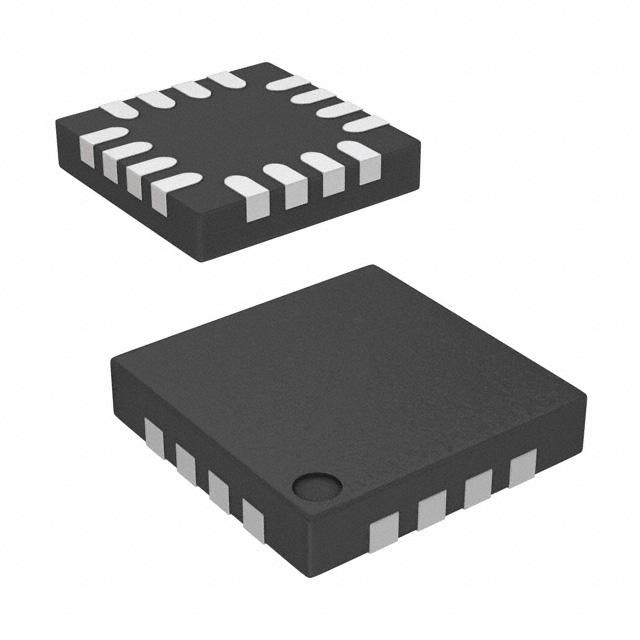


 工商网监
湘ICP备2023018690号
工商网监
湘ICP备2023018690号
